ASIC vs FPGA: A Comprehensive Comparison
As critical components in contemporary computing, choosing between ASICs and FPGAs carries significant implications, underscoring the importance of understanding their unique strengths and trade-offs in the constantly evolving digital landscape.

09 Aug, 2023. 21 minutes read
There's never been a better time to dive into custom chip design, with both FPGA and ASIC design routes being more accessible than ever.
Introduction
ASICs (Application-Specific Integrated Circuits) and FPGAs (Field-Programmable Gate Arrays) are two types of semiconductor devices that serve different purposes in the world of electronics. ASICs are custom-designed for specific applications, offering high performance and efficiency, while FPGAs are reprogrammable devices that provide flexibility and rapid prototyping capabilities. The choice between these two technologies depends on various factors, such as performance requirements, power consumption, cost, design flexibility, and time-to-market.
This article provides a comprehensive comparison of ASICs and FPGAs, delving into their respective advantages and disadvantages, and offering guidance on when to choose one technology over the other. By understanding the key differences between these devices, engineers and designers can make informed decisions that best suit their project requirements and constraints.
What are ASICs?
Definition and Overview
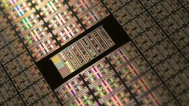
ASICs are specialized semiconductor devices and circuitry designed to perform a specific function or set of functions. Unlike general-purpose processors, such as CPUs and GPUs, ASICs are tailored to meet the requirements of a particular application, resulting in optimized performance and power efficiency. They are typically used in high-volume products where the cost of custom design can be justified by the benefits of improved performance, lower power consumption, and reduced form factor.

ASICs are created through a process called photolithography, where a custom layout of transistors and other components is etched onto a silicon wafer. This layout is designed to implement the desired functionality of the ASIC, which can range from simple logic gates to complex digital signal processing circuits. The manufacturing process for ASICs is time-consuming and expensive, involving multiple steps such as mask creation, wafer fabrication, and packaging. However, once the initial investment is made, the per-unit cost of ASICs decreases significantly as production volume increases.
Further reading: The Ultimate Guide to ASIC Design: From Concept to Production
ASIC Design Process
The ASIC design process consists of several stages, each with its own set of tasks and challenges. The main stages include system specification, design, verification, fabrication, and testing.
System Specification: The first step in the ASIC design process is defining the system requirements and specifications. This involves determining the desired functionality, performance targets, power consumption limits, and other constraints. Engineers and designers collaborate to create a detailed specification document that serves as a blueprint for the ASIC design.
Design: The design stage involves translating the system specifications into a functional ASIC layout. This process typically starts with high-level architectural design, where the overall structure and organization of the ASIC are determined. Next, the design is refined through logic synthesis, which converts the high-level description into a gate-level netlist. The netlist is then optimized for area, power, and performance using various techniques such as technology mapping and placement. Finally, the layout is created through a process called routing, which connects the gates and components on the silicon wafer. The tape out process for ASICs, marking the end of the design phase, is crucial as post-fabrication changes aren't feasible.
Verification: Verification is a critical stage in the ASIC design process, as it ensures that the design meets the system specifications and is free of errors. This stage involves simulating the ASIC design using test vectors and checking for correct functionality, timing, and power consumption. Verification can be performed at various levels of abstraction, from high-level functional verification to low-level gate-level simulations. Formal verification methods, such as model checking and theorem proving, can also be employed to prove the correctness of the design.
Fabrication: Once the design has been verified, it is sent to a semiconductor foundry for fabrication. The fabrication process involves creating a series of photomasks that represent the different layers of the ASIC layout. These masks are used to pattern the silicon wafer through a series of steps, including photolithography, etching, and deposition. The fabricated wafers are then diced into individual ASIC chips and packaged for use in electronic systems.
Testing: The final stage of the ASIC design process is testing, which ensures that the fabricated chips meet the specified performance, power, and reliability requirements. Testing involves applying a set of test vectors to the ASIC and measuring its outputs to verify correct functionality. Additionally, tests for manufacturing defects, such as stuck-at faults and bridging faults, are performed to ensure the quality of the fabricated chips. Once the ASICs have passed all tests, they are ready for integration into electronic systems and deployment in the field.
Before diving into ASIC development, evaluate its necessity. Conduct a Return on Investment (ROI) analysis to ensure that the benefits to your company and customers outweigh the investment risks. For example, if a current PCB costs 20 USD, and a potential ASIC can reduce that to 2 USD, consider the breakeven point against the ASIC's development costs.
It's essential to validate whether your envisioned ASIC functionality and performance are achievable. Many ASIC vendors offer a Feasibility Study service, examining your specifications to determine the project's viability. A detailed ASIC specification document is crucial for obtaining accurate price estimates from design companies.
Advantages of ASICs
Having understood what ASICs are and their prevalent use-cases, it's important to delve into their unique advantages. These benefits make them the technology of choice in several applications, justifying the investment in their custom development. Let's explore these advantages in detail:
High Performance: One of the main advantages of ASICs is their high performance. Since they are custom-designed for a specific application, they can be optimized for maximum efficiency and speed. ASICs often outperform general-purpose processors, such as CPUs and GPUs, in their target applications due to their tailored architecture and dedicated hardware resources.
Low Power Consumption: ASICs are designed with power efficiency in mind, making them suitable for applications where low power consumption is crucial. By optimizing the design for a specific function, ASICs can minimize the number of active components and reduce power consumption compared to general-purpose processors. This is particularly important in battery-powered devices, such as smartphones and IoT sensors, where energy efficiency is a key concern.
Small Form Factor: ASICs can be designed with a compact layout, resulting in a smaller form factor compared to general-purpose processors. This is beneficial in applications where space is limited, such as wearable devices and embedded systems. The reduced size also allows for more efficient cooling and improved thermal performance.
Intellectual Property Protection: Custom ASIC designs can provide a higher level of intellectual property (IP) protection compared to off-the-shelf components. By implementing proprietary algorithms and functionality directly in hardware, companies can safeguard their IP from reverse engineering and unauthorized use.
Cost-Effective for High-Volume Mass Production: Although the initial investment in ASIC design and fabrication can be high, the per-unit cost decreases significantly as production volume increases. This makes ASICs cost-effective for high-volume products, where the benefits of improved performance, lower power consumption, and reduced form factor outweigh the upfront costs.
Integration of Multiple Functions: ASICs can integrate multiple functions and components into a single chip, reducing the need for additional components and simplifying the overall system design. This can lead to reduced system complexity, lower manufacturing costs, and improved reliability.
Disadvantages of ASICs
While ASICs offer significant advantages in certain scenarios, they also have certain limitations that need to be considered during the design and decision-making process. Understanding these disadvantages is critical in evaluating whether an ASIC is the right choice for a given application. Let's delve into these limitations:
High Initial Costs: The design and fabrication of ASICs require significant upfront investment, including costs for design tools, engineering resources, and manufacturing setup. These initial costs can be prohibitive for small companies or projects with limited budgets, making ASICs less attractive for low-volume production.
Long Development Time: The ASIC design process is time-consuming, often taking several months or even years to complete. This extended development time can be a disadvantage in fast-paced industries where rapid product development and time-to-market are critical.
Inflexibility: Once an ASIC is designed and fabricated, its functionality is fixed and cannot be changed without redesigning and manufacturing a new chip. This inflexibility can be a drawback in applications where requirements may change over time or where the ability to update functionality is important.
Obsolescence Risk: Due to the rapid pace of technological advancements in the semiconductor industry, ASICs can become obsolete relatively quickly. This risk of obsolescence can be a concern for companies investing in custom ASIC development, as the return on investment may be diminished if the technology becomes outdated before the product reaches the end of its lifecycle.
Design Complexity: The design of ASICs can be complex, requiring specialized knowledge and expertise in semiconductor design, fabrication, and testing. This complexity can be a barrier for companies without in-house expertise or access to external resources, making it more challenging to develop custom ASIC solutions.
Manufacturing Yield and Reliability: The fabrication of ASICs involves a complex and precise manufacturing process, which can result in yield and reliability issues. Defects in the manufacturing process can lead to non-functional chips or reduced performance, increasing the overall cost and risk associated with ASIC development.
Examples of ASIC
Because of their specialized design, ASICs are often found in a wide range of devices and systems where performance, power efficiency, and form factor are crucial. Here are some common examples of ASIC chips:
Cryptocurrency Mining Hardware: ASICs are widely used in cryptocurrency mining because they can be optimized to perform a specific hashing algorithm (like Bitcoin's SHA-256) much more efficiently than general-purpose computing devices.
Consumer Electronics: Devices such as smartphones, tablets, smart TVs, and game consoles often contain ASICs. These chips are custom-designed to provide the unique functionality of each device, such as graphics rendering, audio processing, and cellular communication.
Telecommunication and Networking Equipment: ASICs are used in a variety of networking equipment such as routers, switches, and modems to handle high-speed data processing tasks efficiently.
Automotive Systems: ASICs are used in various automotive systems, including advanced driver-assistance systems (ADAS), engine control units, and infotainment systems. They provide the necessary computation and control capabilities while meeting stringent automotive standards for reliability and robustness.
Medical Devices: In devices like hearing aids, pacemakers, and imaging systems (like MRI machines), ASICs provide specialized functionality with low power consumption, a crucial feature for battery-operated devices.
Industrial Control Systems: ASICs are often used in industrial control systems to handle specific tasks like motor control, power management, and sensor data processing, providing robust and reliable operation in challenging industrial environments. ASICs can be tailored to act as microcontrollers for specific applications, ensuring optimal performance.
Remember, the common factor across all these examples is the need for optimized, efficient performance for a specific task or set of tasks that justifies the cost and effort of developing a custom ASIC.
What are FPGAs?
Definition and Overview
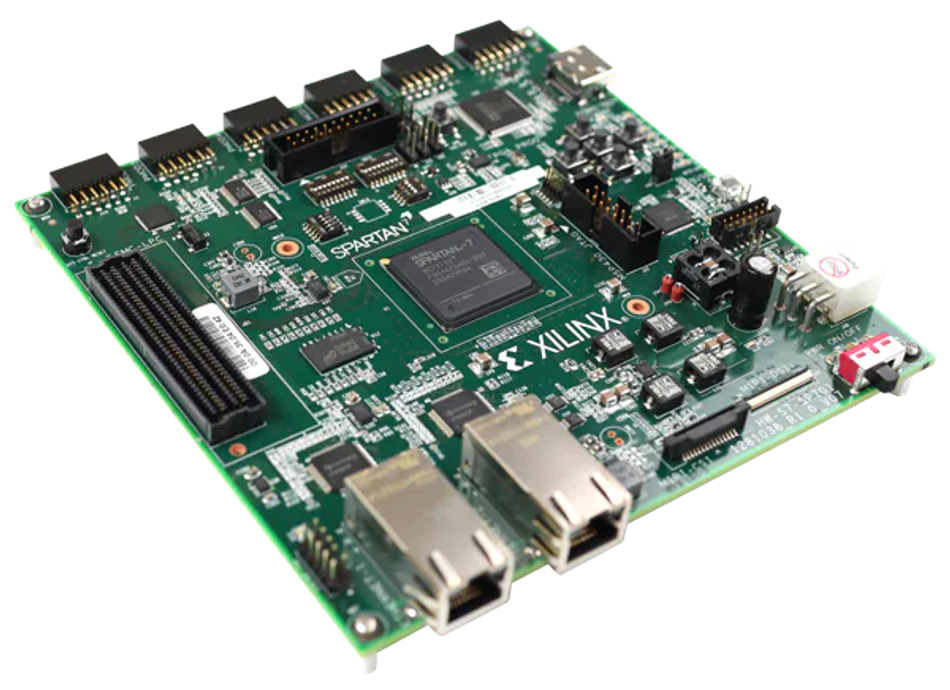
FPGAs are semiconductor devices that can be reprogrammed to implement various digital circuits and functions. Unlike ASICs, which are fixed-function devices, FPGAs offer flexibility and adaptability, allowing designers to modify the functionality of the device even after it has been manufactured. This makes FPGAs an attractive option for rapid prototyping, proof-of-concept development, and applications where design changes are expected.
FPGAs consist of an array of programmable logic blocks and interconnects, which can be configured to implement a wide range of digital circuits, from simple logic gates to complex digital signal processing systems. The programmable logic blocks contain look-up tables (LUTs), flip-flops, and other components that can be used to create custom logic functions. The interconnects, on the other hand, provide the routing infrastructure that connects the logic blocks together, enabling the implementation of larger and more complex circuits. FPGAs, especially those from vendors like AMD-Xilinx, can be equipped with flash memory, enabling data retention even without power.
FPGA programming is typically done using a hardware description language (HDL), such as VHDL or Verilog, which allows designers to describe the desired functionality of the device at a high level of abstraction. The HDL code is then synthesized into a bitstream, which is loaded onto the FPGA to configure the programmable logic blocks and interconnects. This process can be repeated as needed to update or modify the functionality of the FPGA, providing a high degree of design flexibility and adaptability.
Further reading: FPGA Design: A Comprehensive Guide to Mastering Field-Programmable Gate Arrays
FPGA Design Process
The design flow for FPGAs is often more flexible than that of ASICs, allowing for iterative testing and modifications. The FPGA design process involves several stages, including system specification, design entry, synthesis, place and route, and verification.
System Specification: Similar to the ASIC design process, the first step in FPGA design is defining the system requirements and specifications. This involves determining the desired functionality, performance targets, power consumption limits, and other constraints. Engineers and designers collaborate to create a detailed specification document that serves as a blueprint for the FPGA design.
Design Entry: In this stage, the designer creates a high-level description of the desired functionality using a HDL, such as VHDL or Verilog. This HDL code describes the behavior of the digital circuit to be implemented on the FPGA. Alternatively, designers can use schematic entry or graphical design tools to create the design.
Synthesis: The HDL code or schematic is then synthesized into a gate-level netlist, which represents the digital circuit in terms of logic gates and flip-flops. The synthesis process involves mapping the high-level design description to the specific resources available on the target FPGA, such as LUTs, registers, and digital signal processing (DSP) blocks.
Place and Route: The next stage is the place and route process, which assigns the synthesized logic elements to specific locations on the FPGA and determines the routing of interconnects between them. This process aims to optimize the design for area, performance, and power consumption, taking into consideration the constraints and requirements specified in the system specification.
Verification: Verification is a critical stage in the FPGA design process, as it ensures that the design meets the system specifications and is free of errors. This stage involves simulating the FPGA design using test vectors and checking for correct functionality, timing, and power consumption. Verification can be performed at various levels of abstraction, from high-level functional verification to low-level gate-level simulations. Additionally, in-circuit testing and hardware debugging can be performed using FPGA development boards and debugging tools.
Once the design has been verified, the final bitstream is generated and loaded onto the FPGA to configure the programmable logic blocks and interconnects. The FPGA can then be integrated into the target system and deployed in the field. If design changes are required, the FPGA can be reprogrammed with an updated bitstream, providing a high degree of flexibility and adaptability.
Advantages of FPGAs
FPGAs bring a unique set of advantages to the table, particularly in terms of flexibility and adaptability. Let's explore these benefits in more detail:
Design Flexibility: One of the main advantages of FPGAs is their design flexibility. FPGAs can be reprogrammed to implement different digital circuits and functions, allowing designers to modify the functionality of the device even after it has been manufactured. Integration with a variety of peripherals becomes easier with FPGAs due to their design flexibility. This makes FPGAs an attractive option for rapid prototyping, proof-of-concept development, and applications where design changes are expected.
Shorter Time-to-Market: The FPGA design process is generally faster than the ASIC design process, as it does not require the lengthy fabrication and manufacturing steps. This shorter time-to-market allows companies to respond more quickly to changing market demands and technology trends, providing a competitive advantage in fast-paced industries.
Lower Non-Recurring Engineering (NRE) Costs: Unlike ASICs, which require significant upfront investment in design and fabrication, FPGAs have lower NRE costs. This makes FPGAs a more cost-effective option for low-volume production or projects with limited budgets.
Field Upgradability: FPGAs can be reprogrammed in the field, allowing for updates and modifications to be made without the need for physical hardware replacement. This field upgradability can reduce maintenance costs and improve the longevity of electronic systems.
Parallel Processing Capabilities: FPGAs are inherently parallel devices, with multiple programmable logic blocks that can operate independently and concurrently. This parallel processing capability enables FPGAs to excel in applications that require high-speed data processing, such as digital signal processing, image processing, and cryptography.
Adaptability to New Technologies: FPGAs can be reprogrammed to support new technologies and standards as they emerge, making them a future-proof solution for applications that require ongoing updates and enhancements. This adaptability can help companies stay ahead of the competition and extend the life cycle of their products. FPGAs excel in projects requiring a variety of interfaces due to their reconfigurability.
Lower Risk of Obsolescence: Due to their reprogrammable nature, FPGAs have a lower risk of obsolescence compared to ASICs. As technology advances, FPGAs can be updated with new functionality, ensuring that they remain relevant and useful for a longer period of time.
Disadvantages of FPGAs
While FPGAs do have compelling advantages, they also come with a few inherent drawbacks. These drawbacks include:
Lower Performance: FPGAs generally have lower performance compared to ASICs, as they are not optimized for a specific application. The programmable nature of FPGAs introduces overhead in terms of area, power consumption, and performance, making them less suitable for applications that require the highest levels of efficiency and speed.
Higher Power Consumption: Due to their programmable architecture, FPGAs typically consume more power than ASICs. The additional power consumption is a result of the configurable logic blocks, interconnects, and other resources that enable the flexibility of FPGAs. This higher power consumption can be a disadvantage in applications where energy efficiency is a critical concern.
Larger Form Factor: FPGAs tend to have a larger form factor compared to ASICs, as they require additional resources for programmability. This increased size can be a drawback in applications where space is limited or where a compact design is desired.
Higher Unit Cost: While FPGAs have lower NRE costs compared to ASICs, their per-unit cost is generally higher, especially for high-volume production. The higher unit cost is due to the additional resources required for programmability, as well as the lower levels of integration compared to custom ASIC designs.
Design Complexity: FPGA design can be complex, requiring specialized knowledge and expertise in HDLs, synthesis tools, and place-and-route algorithms. This complexity can be a barrier for companies without in-house expertise or access to external resources, making it more challenging to develop FPGA-based solutions.
Limited Resource Availability: FPGAs have a finite number of programmable logic blocks, interconnects, and other resources, which can limit the complexity and functionality of the designs that can be implemented on a single device. In some cases, designers may need to partition their designs across multiple FPGAs or use larger, more expensive devices to accommodate their requirements.
Comparing ASICs and FPGAs
The debate of FPGA vs ASIC centers around the trade-off between design flexibility and performance optimization. But there are several parameters to consider when choosing between the two.
Performance
When comparing the performance of ASICs and FPGAs, it is important to consider the specific application and requirements. In general, ASICs offer higher performance than FPGAs due to their custom design and optimized architecture. Since ASICs are tailored for a specific function, they can be designed to maximize efficiency and speed, resulting in better performance for the target application.
FPGAs, on the other hand, are more flexible and reprogrammable, but this flexibility comes at the cost of performance. The programmable nature of FPGAs introduces overhead in terms of area, power consumption, and performance, as the configurable logic blocks and interconnects are less efficient than the custom-designed components found in ASICs.
However, it is worth noting that the performance gap between ASICs and FPGAs has been narrowing over the years, as advances in FPGA technology have led to improvements in logic density, clock speeds, and on-chip resources. Both ASICs and FPGAs can integrate analog components, such as ADCs, enhancing their functionality beyond purely digital tasks. In some cases, FPGAs can achieve performance levels comparable to ASICs, especially when considering the use of dedicated hardware blocks, such as DSP units and embedded memory.
The choice between ASICs and FPGAs in terms of performance depends on the specific requirements of the application and the trade-offs between performance, flexibility, and cost. For applications that demand the highest levels of efficiency and speed, ASICs may be the preferred choice. However, for applications that require rapid prototyping, design flexibility, or the ability to adapt to changing requirements, FPGAs can offer a viable alternative with competitive performance.
Power Consumption
Power consumption is a critical factor to consider when comparing ASICs and FPGAs, as it can impact the overall efficiency, battery life, and thermal performance of electronic systems. In general, ASICs consume less power than FPGAs due to their custom design and optimized architecture.
ASICs are specifically designed for a particular application, allowing for a high degree of optimization in terms of power consumption. By minimizing the number of active components and tailoring the design to the target function, ASICs can achieve lower power consumption compared to general-purpose processors and FPGAs. This is particularly important in battery-powered devices and energy-sensitive applications, where power efficiency is a key concern.
FPGAs, on the other hand, have higher power consumption due to their programmable nature. The configurable logic blocks, interconnects, and other resources that enable the flexibility of FPGAs introduce overhead in terms of power consumption. Additionally, FPGAs typically operate at lower clock frequencies compared to ASICs, which can result in higher dynamic power consumption for certain applications.
However, it is worth noting that advances in FPGA technology have led to improvements in power efficiency, with newer devices featuring lower static power consumption, more efficient interconnects, and advanced power management features. In some cases, FPGAs can achieve power consumption levels comparable to ASICs, especially when considering the use of dedicated hardware blocks and optimized design techniques.
When comparing ASICs and FPGAs in terms of power consumption, it is essential to consider the specific requirements of the application and the trade-offs between power efficiency, flexibility, and cost. For applications that demand the lowest power consumption, ASICs may be the preferred choice. However, for applications that require design flexibility or the ability to adapt to changing requirements, FPGAs can offer a viable alternative with competitive power consumption levels.
Cost
Cost is an important factor when comparing ASICs and FPGAs, as it can impact the overall affordability and return on investment of a project. The cost differences between these two technologies can be attributed to factors such as NRE costs, per-unit costs, and manufacturing complexity.
Non-Recurring Engineering Costs: ASICs have high NRE costs due to the custom design, fabrication, and manufacturing setup required for each unique design. These upfront costs can be prohibitive for small companies or projects with limited budgets, making ASICs less attractive for low-volume production. In contrast, FPGAs have lower NRE costs, as they do not require custom fabrication and can be reprogrammed to implement different designs using the same device.
Per-Unit Costs: While FPGAs have lower NRE costs, their per-unit costs are generally higher than those of ASICs, especially for high-volume production. The higher unit cost of FPGAs is due to the additional resources required for programmability, as well as the lower levels of integration compared to custom ASIC designs. However, for low-volume production or projects with rapidly changing requirements, the higher per-unit cost of FPGAs may be offset by the lower NRE costs and design flexibility.
Manufacturing Complexity: The manufacturing process for ASICs is more complex and time-consuming than that of FPGAs, which can impact the overall cost and lead time of a project. ASIC fabrication involves multiple steps, such as mask creation, wafer fabrication, and packaging, which can result in higher costs and longer lead times. FPGAs, on the other hand, can be purchased off-the-shelf and reprogrammed as needed, reducing manufacturing complexity and lead time.
When comparing ASICs and FPGAs in terms of cost, it is essential to consider the specific requirements of the application and the trade-offs between upfront investment, per-unit costs, and design flexibility. For high-volume production or applications that demand the lowest per-unit cost, ASICs may be the preferred choice. However, for low-volume production or projects with rapidly changing requirements, FPGAs can offer a cost-effective alternative with lower NRE costs and greater design flexibility.
Design Flexibility
Design flexibility is a key factor when comparing ASICs and FPGAs, as it can impact the ability to adapt to changing requirements and accommodate new features or functionality. The main differences in design flexibility between these two technologies stem from their respective architectures and programmability.
ASICs: As custom-designed devices, ASICs offer limited design flexibility once they have been fabricated. Any changes to the functionality or features of an ASIC require a new design and fabrication process, which can be time-consuming and expensive. This inflexibility can be a disadvantage in applications where requirements may change over time or where the ability to update functionality is important. However, the custom nature of ASICs allows for highly optimized designs that can provide superior performance, power efficiency, and form factor compared to FPGAs.
FPGAs: FPGAs, on the other hand, offer a high degree of design flexibility due to their programmable architecture. The configurable logic blocks and interconnects in FPGAs can be reprogrammed to implement different digital circuits and functions, allowing designers to modify the functionality of the device even after it has been manufactured. This flexibility makes FPGAs an attractive option for rapid prototyping, proof-of-concept development, and applications where design changes are expected or the ability to adapt to new technologies and standards is crucial.
When comparing ASICs and FPGAs in terms of design flexibility, it is important to consider the specific requirements of the application and the trade-offs between performance, power efficiency, and adaptability. For applications that demand the highest levels of optimization and fixed functionality, ASICs may be the preferred choice. However, for applications that require design flexibility, the ability to accommodate changing requirements, or rapid prototyping capabilities, FPGAs can offer a more suitable solution.
Time-to-Market
Time-to-market is an important consideration when comparing ASICs and FPGAs, as it can impact the competitiveness and success of a product in the marketplace. The main differences in time-to-market between these two technologies stem from their respective design, fabrication, and verification processes.
ASICs: The ASIC design process is time-consuming, often taking several months or even years to complete. This extended development time includes the design, verification, fabrication, and testing stages, which can be a disadvantage in fast-paced industries where rapid product development and time-to-market are critical. Additionally, any changes to the ASIC design require a new fabrication process, further extending the time-to-market.
FPGAs: In contrast, the FPGA design process is generally faster than the ASIC design process, as it does not require the lengthy fabrication and manufacturing steps. FPGAs can be purchased off-the-shelf and programmed with the desired functionality, allowing for rapid prototyping and shorter development cycles. Furthermore, design changes can be implemented by reprogramming the FPGA, without the need for a new fabrication process. This shorter time-to-market allows companies to respond more quickly to changing market demands and technology trends, providing a competitive advantage in fast-paced industries.
Below is a comparison table between ASICs and FPGAs, providing a detailed overview of their distinct features and applications.
Comparison Point | ASICs | FPGAs |
Design Flexibility | Limited once fabricated; changes require new design and fabrication | High due to programmability; can be modified post-manufacturing; suitable for rapid prototyping and adaptive designs |
Performance | Higher due to custom design; optimized for specific application | Somewhat lower due to reconfigurable architecture; has a performance overhead due to programmability |
Power Consumption | Typically lower due to optimized design | Generally higher than ASICs, especially in large designs |
Time-to-Market | Longer due to design, verification, fabrication, and testing stages; changes further extend time | Shorter; does not require lengthy fabrication; design changes can be quickly implemented by reprogramming |
Cost | Lower per-unit cost for high-volume production; higher Non-Recurring Engineering (NRE) costs | Higher per-unit cost for low-volume production; lower NRE costs |
Applications | Preferred for high-volume, fixed-function applications with high performance and power efficiency requirements | Preferred for rapid prototyping, changing requirements, low-volume production, or projects with limited budgets |
Integration with SoCs | Some modern SoCs might have ASIC-based microprocessors | Some modern SoCs might contain FPGA elements for flexibility |
Longevity & Reliability | Generally longer lifespan due to reduced susceptibility to environmental factors like radiation | May have a reduced lifespan in certain applications due to sensitivity to factors like radiation and high heat |
Development Tools | Requires specialized design and verification tools, which can be expensive | Broad ecosystem of tools available, both from FPGA vendors and third-party suppliers; more user-friendly development environments |
Custom IP Protection | Stronger protection since the design is hard-wired and cannot be easily reverse-engineered | Vulnerable to potential IP theft or cloning, especially if design security measures aren't rigorously implemented |
Reusability | Not reusable; once fabricated, the design is set | Highly reusable; the same FPGA can be reprogrammed for multiple applications or iterations |
Initial Investment | High initial investment due to design, verification, and tooling costs | Lower initial investment; primarily just the cost of the FPGA and development tools |
Table 1: Comparison between ASICs and FPGAs
When comparing ASICs and FPGAs in terms of time-to-market, it is important to consider the specific requirements of the application and the trade-offs between development time, performance, and cost. For applications that demand the highest levels of optimization and fixed functionality, ASICs may be the preferred choice, despite their longer development time. However, for applications that require rapid prototyping, design flexibility, or the ability to adapt to changing requirements, FPGAs can offer a more suitable solution with shorter time-to-market.
Further reading: Wafer Backgrinding: An In-Depth Guide to Semiconductor Manufacturing
Choosing Between ASICs and FPGAs
Factors to Consider
When deciding between ASICs and FPGAs for a particular application, several factors should be taken into account to ensure the best choice is made. These factors include:
Performance: Evaluate the performance requirements of the application and determine whether the optimized performance of an ASIC or the flexibility of an FPGA is more suitable. ASICs generally offer higher performance due to their custom design, while FPGAs provide reprogrammability at the cost of some performance overhead.
Power Consumption: Consider the power consumption constraints of the application and the impact of the chosen technology on overall system efficiency. ASICs typically consume less power than FPGAs due to their optimized design, making them a better choice for energy-sensitive applications.
Cost: Assess the budget and production volume of the project to determine whether the lower per-unit cost of ASICs or the lower NRE costs of FPGAs are more advantageous. ASICs may be more cost-effective for high-volume production, while FPGAs can be a better option for low-volume production or projects with limited budgets.
Design Flexibility: Determine the importance of design flexibility and the ability to accommodate changing requirements or update functionality. FPGAs offer greater design flexibility due to their reprogrammable nature, making them a more suitable choice for applications that require rapid prototyping or adaptability.
Time-to-Market: Consider the time-to-market requirements of the project and the impact of the chosen technology on development time and lead time. FPGAs generally have a shorter time-to-market compared to ASICs, as they do not require custom fabrication and can be reprogrammed as needed.
By carefully evaluating these factors and weighing the trade-offs between performance, power consumption, cost, design flexibility, and time-to-market, engineers and designers can make an informed decision on whether to choose an ASIC or FPGA for their specific application.
Conclusion
In summary, the choice between ASICs and FPGAs depends on various factors, such as performance, power consumption, cost, design flexibility, and time-to-market. ASICs offer higher performance, lower power consumption, and smaller form factors, making them suitable for high-volume production and applications that demand optimized efficiency. FPGAs, on the other hand, provide design flexibility, reprogrammability, and shorter time-to-market, making them ideal for rapid prototyping, proof-of-concept development, and applications with changing requirements. Some modern SoCs (System on Chips) might contain both FPGA elements and ASIC-based microprocessors, blending flexibility with optimized performance. By carefully evaluating these factors and considering the specific needs of the application, engineers and designers can make informed decisions on whether to choose an ASIC or FPGA for their project.
Frequently Asked Questions (FAQs)
1. What is the main difference between ASICs and FPGAs?
The main difference between ASICs and FPGAs is that ASICs are custom-designed, fixed-function devices optimized for a specific application, while FPGAs are reprogrammable devices that can be configured to implement various digital circuits and functions.
2. When should I choose an ASIC over an FPGA?
ASICs are generally preferred for high-volume production, applications that demand the highest levels of performance and power efficiency, and situations where a custom design can provide significant advantages in terms of form factor and intellectual property protection.
3. When should I choose an FPGA over an ASIC?
FPGAs are typically chosen for rapid prototyping, proof-of-concept development, and applications with changing requirements or the need for design flexibility. They are also suitable for low-volume production or projects with limited budgets, as they have lower NRE costs compared to ASICs.
4. Can FPGAs be used as a stepping stone to ASIC development?
Yes, FPGAs can be used as a stepping stone to ASIC development. Designers can use FPGAs for rapid prototyping and validation of their designs before transitioning to ASICs for high-volume production. This approach can help reduce development risks and costs by allowing designers to refine and optimize their designs before committing to the expensive ASIC fabrication process.
5. Are there any alternatives to ASICs and FPGAs?
Other alternatives to ASICs and FPGAs include general-purpose processors, such as CPUs and GPUs, as well as application-specific standard products (ASSPs), which are pre-designed integrated circuits tailored for specific applications but not as customized as ASICs. The choice between these technologies depends on factors such as performance, power consumption, cost, and design flexibility.
References
[1] Harris D, Harris SL. Digital Design and Computer Architecture. Elsevier Science; 2013. [Online] Available from: https://www.google.co.in/books/edition/Digital_Design_and_Computer_Architecture/-DG18Nf7jLcC
[2] Infineon. Infineon customized solutions for a wide-range of applications [Online]. Available from: https://www.infineon.com/cms/en/product/asic/
[3] Intel. Comparing FPGAs, Structured ASICs, and Cell-Based ASICs [Online]. Available from: https://www.intel.com/content/www/us/en/products/programmable/fpga-vs-structured-asic.html