Arduino Mega 2560 Pinout: A Complete Engineering Reference
Arduino Mega 2560 pinout guide: 54 digital pins, 16 analog inputs, 4 UARTs, the PWM timer map, ATmega2560 port mapping, and current limits.

12 Aug, 2026. 19 minutes read
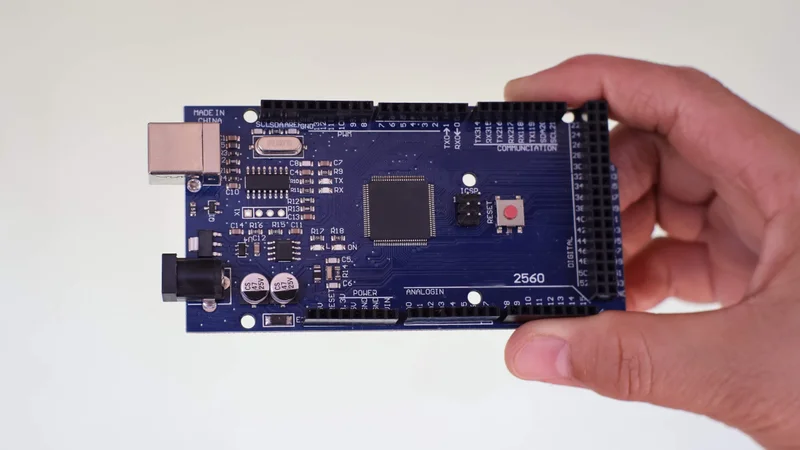
Arduino Mega 2560 Rev3 microcontroller board
Key Takeaways
The Arduino Mega 2560 pinout exposes 54 digital I/O pins (15 PWM capable), 16 analog inputs, four hardware UARTs, one I2C bus, and one SPI bus from a 100-pin ATmega2560 running at 16 MHz.
Arduino rates each I/O pin at a maximum of 20 mA, while the ATmega2560 silicon absolute maximum is 40 mA. Design to 20 mA, and never treat 40 mA as a target.
The 200 mA and 100 mA limits are per port group, not per board. Digital pins 0 to 5 share a single 100 mA budget, which catches people who drive several LEDs from the low pin numbers.
Fourteen of the 15 PWM pins run at roughly 490 Hz. Pins 4 and 13 run at roughly 976 Hz because Timer0 also drives millis() and delay().
Migrating an Uno sketch is not plug and play: SPI moves from pins 11 to 13 over to pins 50 to 52, and I2C moves from A4/A5 to pins 20 and 21.
Introduction
The Arduino Mega 2560 pinout is what you reach for when an Uno runs out of room. This microcontroller board breaks out 54 digital input/output pins, 16 analog inputs, and four hardware serial ports, which is why it became the default controller for 3D printers, multi-axis robotics, and any project that needs to talk to a dozen peripherals at once.2
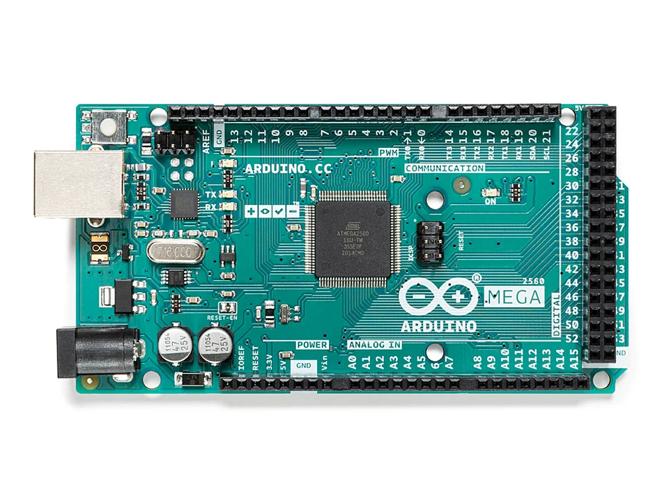
But reading the Arduino Mega 2560 pinout off a diagram isn't enough to keep a design inside spec. On the Arduino Mega 2560 pinout, pins share timers, share current budgets, and share peripheral blocks; two pins that look identical on the Arduino Mega 2560 pinout diagram can behave very differently once you enable PWM on one of them, or once you push both past their shared port's current limit. Get the Arduino Mega 2560 pinout wrong at the port level, and the symptom shows up as a flickering LED or a corrupted SPI transfer, not a compile error.
This guide works through the Arduino Mega 2560 pinout by function, then maps every header pin back to its ATmega2560 port. Every number here comes from the official Arduino Mega 2560 Rev3 datasheet 1, the Microchip ATmega2560 datasheet 4, or the Arduino AVR core source.14
Arduino Mega 2560 Specifications
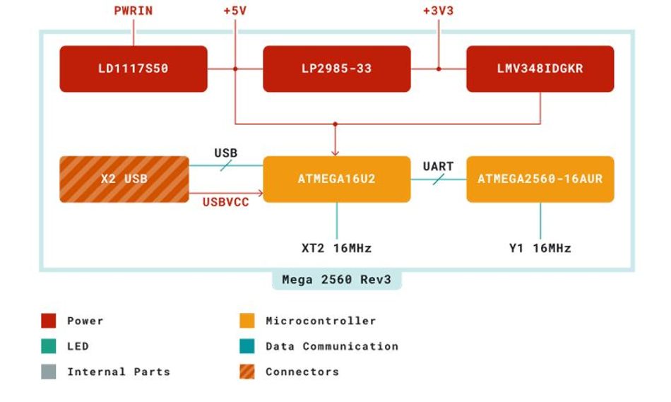
The Mega 2560 Rev3 pairs an ATmega2560 microcontroller with an ATmega16U2 acting as the USB-to-serial converter. The ATmega16U2 handles the USB connection, which is why digital pins 0 and 1 are not fully yours to use.
Parameter | Value |
Microcontroller | ATmega2560, 16 MHz, up to 16 MIPS |
USB-to-serial converter | ATmega16U2 (16 KB flash, 512 B SRAM, 512 B EEPROM) |
Digital I/O pins | 54 (15 PWM capable) |
Analog input pins | 16 (A0 to A15), 10-bit ADC |
Hardware UARTs | 4 |
Flash memory | 256 KB, of which 8 KB is bootloader (253,952 bytes usable) 2 |
SRAM | 8 KB (8,192 bytes) |
EEPROM | 4 KB |
Operating voltage | 5 V |
Input voltage, recommended (VIN or power jack) | 7 V to 12 V |
Input voltage, limit | 6 V to 20 V |
USB input voltage | 4.8 V to 5.5 V |
Max current per I/O pin | 20 mA |
Max current from the 3.3 V pin | 50 mA |
Operating temperature | -40 °C to +85 °C |
The usable sketch size of 253,952 bytes and the 8,192-byte SRAM figure come straight from the boards.txt definition in the Arduino AVR core, so they match exactly what the IDE reports when you compile.12
Complete Arduino Mega 2560 Pin Reference Table
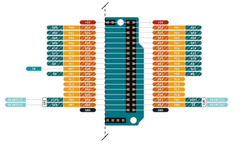
Use this as the lookup table.3 Every digital pin is listed with the ATmega2560 port bit behind it and every alternate function it carries. The sections after it explain what the conflicts mean in practice.
Arduino pin | ATmega2560 port | Alternate functions |
D0 | PE0 | RX0 (Serial), PCINT8 |
D1 | PE1 | TX0 (Serial) |
D2 | PE4 | PWM (OC3B), INT4 |
D3 | PE5 | PWM (OC3C), INT5 |
D4 | PG5 | PWM (OC0B) |
D5 | PE3 | PWM (OC3A) |
D6 | PH3 | PWM (OC4A) |
D7 | PH4 | PWM (OC4B) |
D8 | PH5 | PWM (OC4C) |
D9 | PH6 | PWM (OC2B) |
D10 | PB4 | PWM (OC2A), PCINT4 |
D11 | PB5 | PWM (OC1A), PCINT5 |
D12 | PB6 | PWM (OC1B), PCINT6 |
D13 | PB7 | PWM (OC0A / OC1C), PCINT7, LED_BUILTIN |
D14 | PJ1 | TX3 (Serial3), PCINT10 |
D15 | PJ0 | RX3 (Serial3), PCINT9 |
D16 | PH1 | TX2 (Serial2) |
D17 | PH0 | RX2 (Serial2) |
D18 | PD3 | TX1 (Serial1), INT3 |
D19 | PD2 | RX1 (Serial1), INT2 |
D20 | PD1 | SDA (I2C), INT1 |
D21 | PD0 | SCL (I2C), INT0 |
D22 to D29 | PA0 to PA7 | External memory bus AD0 to AD7 |
D30 to D37 | PC7 down to PC0 | External memory bus A15 down to A8 |
D38 | PD7 | Timer0 external clock (T0) |
D39 | PG2 | External memory address latch (ALE) |
D40 | PG1 | External memory read strobe (RD) |
D41 | PG0 | External memory write strobe (WR) |
D42 | PL7 | None |
D43 | PL6 | None |
D44 | PL5 | PWM (OC5C) |
D45 | PL4 | PWM (OC5B) |
D46 | PL3 | PWM (OC5A) |
D47 | PL2 | Timer5 external clock (T5) |
D48 | PL1 | Input capture (ICP5) |
D49 | PL0 | Input capture (ICP4) |
D50 | PB3 | CIPO / MISO (SPI), PCINT3 |
D51 | PB2 | COPI / MOSI (SPI), PCINT2 |
D52 | PB1 | SCK (SPI), PCINT1 |
D53 | PB0 | CS / SS (SPI), PCINT0 |
A0 to A7 (D54 to D61) | PF0 to PF7 | ADC0 to ADC7. PF4 to PF7 also carry JTAG, disabled by fuse. |
A8 to A15 (D62 to D69) | PK0 to PK7 | ADC8 to ADC15, PCINT16 to PCINT23 |
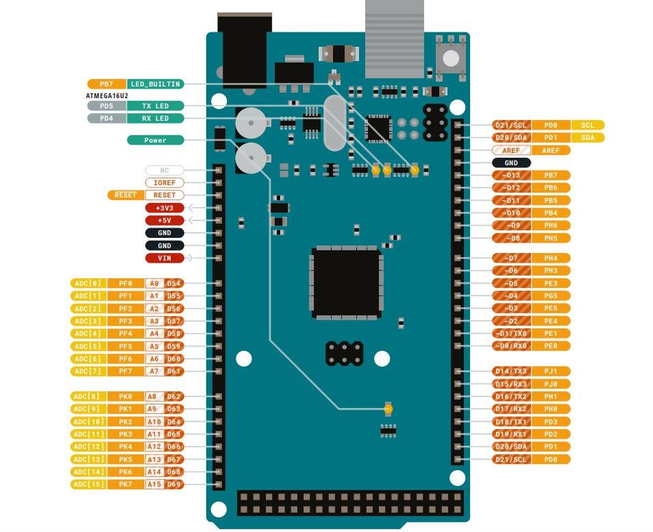
Two rows in that table are ordered in reverse for a reason. D30 to D37 map to PC7 down to PC0, so D30 is PC7 and D37 is PC0. The same inversion applies to D42 to D49 against PL7 down to PL0. 2
Recommended Reading: Arduino Nano Pinout: Complete Technical Reference
Power Pins and Electrical Limits
The power header sits on the short edge of the board, next to the analog inputs. These pins are the ones most likely to release smoke if you get them wrong, so they are worth understanding before anything else.
Pin | Type | What it does |
VIN | Power in or out | Raw supply from the power jack, or an input for an unregulated supply. Recommended 7 V to 12 V. |
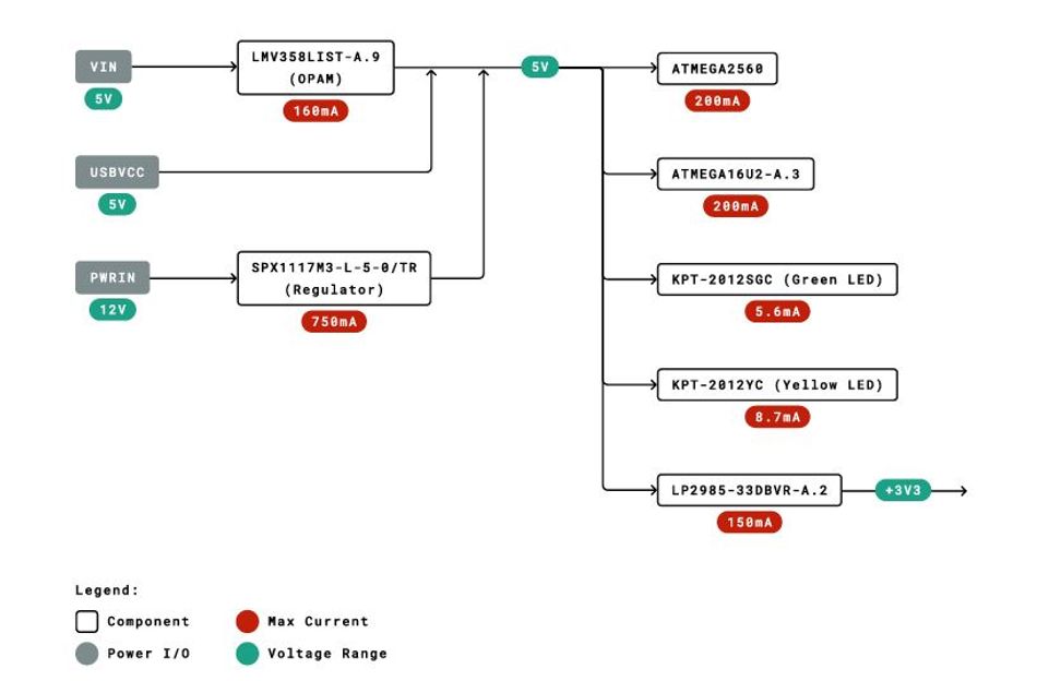
5V | Power out | Regulated rail at 5 volts, feeding the ATmega2560 and the shield header. |
3V3 | Power out | Regulated 3.3 V rail. Maximum 50 mA. 2 |
GND | Ground | Multiple ground pins, all common. |
IOREF | Reference | Reports the board logic voltage to a shield. Connected to 5 V on the Mega 2560. |
RESET | Control | Pull low to reset, the same action as the onboard reset button. Has an internal pull-up of 30 kΩ to 60 kΩ. |
AREF | Reference | External ADC reference input. |
Two different input voltage numbers circulate, and they are not in conflict. Arduino specifies 7 V to 12 V as the recommended range and 6 V to 20 V as the limit. Below 7 V, the regulator drops out under load, and the rail falls short of 5 volts. 1 Above 12 V, it dissipates enough heat to become the limiting component, even though the board survives to 20 V.
The barrel connector is a 2.1 mm center-positive power jack. Powering through it or through VIN engages the onboard regulator, while USB power bypasses it, so a board that behaves differently on USB than on the power jack is usually telling you about a regulator or supply problem.
The reset button pulls the same RESET line that the pin exposes. The ATmega16U2 also drives that line from its DTR flow control signal, which is how the IDE resets the board automatically when it starts an upload.
Per-Pin and Per-Port Current Limits
This is where most Arduino Mega 2560 pinout references stop short. Arduino specifies 20 mA maximum per I/O pin. The ATmega2560 datasheet lists 40 mA as the absolute maximum rating per I/O pin, and absolute maximum ratings are stress limits, not operating conditions.1
The reason 20 mA is the working number is in the DC characteristics table. Output voltage is only guaranteed at that load: with a 5 V supply, a pin sourcing 20 mA is specified to stay above 4.2 V, and a pin sinking 20 mA is specified to stay below 0.9 V. Push past that and your logic levels drift.
The limit that actually bites is the group budget. The ATmega2560 datasheet caps the sum of currents across defined port groups, and those groups map onto the Arduino header in a distinctly non-obvious way. 4
ATmega2560 port group | Arduino pins in the group | Total current limit |
PJ0-PJ7, PA0-PA7, PG2 | D14, D15, D22 to D29, D39 | 200 mA |
PC0-PC7, PG0-PG1, PD0-PD7, PL0-PL7 | D18 to D21, D30 to D38, D40, D41, D42 to D49 | 200 mA |
PG3-PG4, PB0-PB7, PH0-PH7 | D6 to D13, D16, D17, D50 to D53 | 200 mA |
PE0-PE7, PG5 | D0 to D5 | 100 mA |
PF0-PF7, PK0-PK7 | A0 to A15 | 100 mA |
Read the fourth row again. Digital pins 0 through 5, the block most people wire up first, share a single 100 mA budget. Six pins at 20 mA each is 120 mA, which is already over the limit. Spread high-current loads across groups, or better, drive them through transistors or a driver IC.
Digital I/O Pins (D0 to D53)
Digital pins read or write a simple on/off signal, HIGH or LOW; which is the basic building block for buttons, LEDs, relays, and most simple sensors. All 54 digital pins operate at 5 V logic and are driven with digitalWrite() and read with digitalRead() after you set their direction with pinMode(). Each has a software-selectable internal pull-up resistor, specified at 20 kΩ to 50 kΩ, which you enable with pinMode(pin, INPUT_PULLUP).
A pin reading HIGH needs at least 0.6 times the operating voltage on a 5 V board, which is 3.0 V, and reads LOW below 0.3 times the operating voltage, or 1.5 V. Between those thresholds the result is undefined, which is why a floating input read with digitalRead() returns noise rather than a stable value.
That tolerance range matters for anything time-sensitive. A 50 kΩ pull-up against a few hundred picofarads of cable capacitance gives a noticeably slow rising edge, so use an external pull-up of 4.7 kΩ or lower for fast signals or long wires.
Pins D22 to D53 sit on the dual-row header at the end of the board, and the numbering alternates between the rows. The left row carries the even pins D22 to D52, the right row carries the odd pins D23 to D53, and each row is bracketed by a 5 V pin at one end and a ground pin at the other.1
Pin D13 drives the onboard LED through a resistor, which is exposed in code as LED_BUILTIN. Because the LED and its driver load the pin, D13 is a poor choice for an input, and a poor choice for a signal you need to be electrically clean.
PWM Pins and the Timer Map
The Mega 2560 has 15 PWM pins: D2 to D13, plus D44, D45, and D46. On the silkscreen, they are marked with a tilde. analogWrite() takes a value from 0 to 255 regardless of the underlying timer resolution.8
What the pinout diagram does not show is that these 15 pins are driven by six different timers, and pins sharing a timer share its configuration. If you change a timer's prescaler to alter PWM frequency, every pin on that timer changes with it.9
Timer | Width | Output compare | Arduino pin | Default frequency |
Timer0 | 8-bit | OC0A | D13 | 976 Hz |
Timer0 | 8-bit | OC0B | D4 | 976 Hz |
Timer1 | 16-bit | OC1A / OC1B / OC1C | D11 / D12 / D13 | 490 Hz |
Timer2 | 8-bit | OC2A / OC2B | D10 / D9 | 490 Hz |
Timer3 | 16-bit | OC3A / OC3B / OC3C | D5 / D2 / D3 | 490 Hz |
Timer4 | 16-bit | OC4A / OC4B / OC4C | D6 / D7 / D8 | 490 Hz |
Timer5 | 16-bit | OC5A / OC5B / OC5C | D46 / D45 / D44 | 490 Hz |
Those frequencies are not arbitrary. The Arduino AVR core's init() routine sets every timer to a prescaler of 64. Timer0 is configured for fast PWM with an 8-bit top value, giving 16,000,000 / (64 × 256) = 976.6 Hz. Timers 1 through 5 are configured for 8-bit phase-correct PWM, which takes twice as long per cycle, giving 16,000,000 / (64 × 510) = 490.2 Hz.9
Two consequences follow directly from that table.
Timer0 also runs the clock. millis(), micros(), and delay() are all built on Timer0. Reprogramming Timer0 to change the PWM frequency on D4 or D13 will break Arduino timekeeping across your whole sketch. Arduino documents the same interaction on the Uno's Timer0 pins (5 and 6): low duty-cycle values may not fully switch off the output. The same mechanism applies to D4 and D13 here, since the same timer drives them. 3
D13 is double-booked. The ATmega2560 pin behind D13 carries both OC0A and OC1C. Arduino drives it from Timer0, so D13 runs at 976 Hz while D11 and D12 on the same Timer1 run at 490 Hz.
If you need a specific PWM frequency, for a motor driver or an LED dimmer above the flicker threshold, pick a pin on Timer3, Timer4, or Timer5. Those are 16-bit timers; none of them backs a core Arduino function, and reconfiguring them costs you nothing else.
Recommended Reading: What Is a PWM Signal? Fundamentals and Practical Applications for Engineers
Analog Input Pins (A0 to A15)
Analog inputs let you read a variable voltage, not just on/off. That is how you measure things like a potentiometer's position, a light sensor's brightness, or a temperature sensor's output. The Mega 2560 brings out 16 analog inputs to a single header. Each feeds a 10-bit successive approximation ADC, so analogRead() returns 0 to 1023. Against the default 5 V reference, that is a resolution of about 4.88 mV per count.
The 16 inputs come from two different ports, which matters if you use direct port manipulation. A0 to A7 are PF0 to PF7, and A8 to A15 are PK0 to PK7.
Every analog pin also works as a general-purpose digital pin. In code, you can address them as A0 to A15 or by their digital aliases, D54 to D69, which the official pinout diagram shows alongside the analog labels.
Selecting an ADC Reference
analogReference() selects what the ADC measures against. The ATmega2560 offers the 5 V supply by default, two internal bandgap references at 1.1 V and 2.56 V, and an external reference applied to the AREF pin.
There is a hardware hazard here worth stating plainly. The ATmega2560 datasheet notes that internal reference options must not be used while an external voltage is applied to AREF.4 If you have wired a reference to AREF and then select an internal reference in software, you short the internal reference against your external source. Call analogReference(EXTERNAL) before your first analogRead(), and keep a 5 kΩ resistor in series with AREF as insurance.
ADC Speed and Source Impedance
Two ADC limits decide whether your readings are trustworthy, and neither appears on a pinout diagram.
The first is source impedance. The ATmega2560 datasheet states the ADC is optimized for sources of approximately 10 kΩ or less. Above that, the sample-and-hold capacitor does not fully charge within the sampling window, and readings come back low and noisy. This is why a high-value potentiometer or a resistor divider built from megaohm resistors gives unstable results, and why a buffer op-amp fixes them.4
The second is conversion time. The Arduino core sets the ADC prescaler to 128, giving a 125 kHz ADC clock from the 16 MHz system clock, which sits inside the 50 kHz to 200 kHz band the datasheet requires for full 10-bit resolution. A single-ended conversion takes 13 ADC clock cycles, so each analogRead() costs about 104 µs.
Parameter | Value on a stock Mega 2560 |
Resolution | 10-bit (0 to 1023) |
ADC clock | 125 kHz (16 MHz with prescaler 128) |
Conversion time | About 104 µs per analogRead() |
Practical sample rate | Roughly 9,600 samples per second |
Recommended source impedance | 10 kΩ or less |
Input voltage range | 0 V to VCC |
Absolute accuracy | ±2 LSB |
That 104 µs matters more than it looks. Reading all 16 analog inputs in a loop costs about 1.7 ms, which is a significant chunk of a fast control loop. If you need more speed and can live with fewer bits, the datasheet allows an ADC clock up to 1000 kHz at reduced resolution.
Why A4 to A7 Are Free on the Mega
On the ATmega2560, pins PF4 to PF7 double as the JTAG debug interface (TCK, TMS, TDO, and TDI). If JTAG is enabled, those four pins are not available as analog inputs.
They work on the Mega because of a fuse setting. The Arduino AVR core programs the ATmega2560 with a high fuse byte of 0xD8. 12 Bit 6 of that byte is JTAGEN, and it is left unprogrammed, which disables JTAG. That is why A4 to A7 behave like any other analog input on a stock board, and why they stop working if you re-enable JTAG with an external programmer.
Serial (UART) Pins: Four Hardware Ports
Four hardware UARTs is the single biggest reason to choose a Mega over an Uno. You can run a GPS module, a serial LCD, a radio module, and the USB debug console at the same time without a software serial library and without timing compromises.
Port | RX pin | TX pin | ATmega2560 pins | Notes |
Serial | D0 | D1 | PE0 / PE1 | Shared with the ATmega16U2 USB bridge |
Serial1 | D19 | D18 | PD2 / PD3 | Fully free |
Serial2 | D17 | D16 | PH0 / PH1 | Fully free |
Serial3 | D15 | D14 | PJ0 / PJ1 | Fully free |
Note the pin ordering. On Serial1, Serial2, and Serial3, the RX pin has the higher number and TX the lower, which is the reverse of Serial on D0 and D1. Wiring a module by pattern rather than by label is a common way to end up with a silent link.
Keep external hardware off D0 and D1 wherever you can. Those pins are wired to the ATmega16U2, so anything driving them will interfere with sketch uploads and with the Serial Monitor.
Recommended Reading: ATmega328P: Pinout, Registers, Fuses, and Arduino Pin Mapping
I2C Pins: D20 (SDA) and D21 (SCL)
I2C is a two-wire protocol that lets you address multiple sensors or displays on the same bus using unique device addresses, at the cost of speed compared to SPI. I2C on the Mega 2560 lives on D20 for SDA and D21 for SCL, driven through the Wire library.11 The same signals are also duplicated on the dedicated SDA and SCL pins next to AREF on the digital header.
The Mega 2560 has pull-up resistors on pins 20 and 21 on the board, so a simple sensor bus often works with no external pull-ups at all. On a long bus or with many devices, you may still want stronger external pull-ups, and you should account for the onboard ones already being in parallel.
Those onboard pull-ups have a side effect. Arduino documents that pins 20 and 21 "have external pull-ups that cannot be disabled", which makes them a poor choice for anything expecting a clean high impedance input, even when you are not using I2C.6
SPI Pins: D50 to D53 and the ICSP Header
SPI is a fast, synchronous protocol for talking to peripherals like SD cards, displays, and sensors over short distances, using separate lines for data in, data out, and clock. The SPI bus is on four dedicated pins, and this is where Uno code most often breaks.
Signal | Mega 2560 pin | Uno R3 pin | ATmega2560 pin |
CIPO (MISO) | D50 | D12 | PB3 |
COPI (MOSI) | D51 | D11 | PB2 |
SCK | D52 | D13 | PB1 |
CS (SS) | D53 | D10 | PB0 |
The same SPI signals also appear on the six-pin ICSP header near the center of the board, in the same position as on the Uno. This is the escape hatch for shield compatibility: a shield that takes SPI from the ICSP header works on both boards, while a shield hard-wired to pins 11, 12, and 13 will not work on the Mega without jumpers.6
D53 deserves special attention. Even if you drive chip select from a different pin, D53 must be configured as an output for the hardware SPI peripheral to stay in controller mode. Leave it as an input, pull it low, and the peripheral switches to target mode and your bus stops working.
Recommended Reading: I2C vs SPI vs UART: A Comprehensive Comparison
ICSP Header Pinouts
The Mega 2560 has two ICSP headers, and confusing them is a common way to brick an afternoon. The main ICSP header near the middle of the board programs the ATmega2560. The second header, marked ICSP1 and sitting next to the USB connector, programs the ATmega16U2 USB bridge.1
Both use the standard six-pin AVR layout in two rows of three.
ICSP pin | Signal | Main ICSP (ATmega2560) | ICSP1 (ATmega16U2) |
1 | CIPO / MISO | D50 (PB3) | ATmega16U2 internal |
2 | +5V | 5 V rail | 5 V rail |
3 | SCK | D52 (PB1) | ATmega16U2 internal |
4 | COPI / MOSI | D51 (PB2) | ATmega16U2 internal |
5 | RESET | ATmega2560 reset | ATmega16U2 reset |
6 | GND | Ground | Ground |
Use the main ICSP header for two things: burning a bootloader with an external programmer, and giving a shield access to SPI without occupying pins 50 to 52. Because it sits in the same position on the Mega as on the Uno, it is the only SPI connection that is mechanically compatible between the two boards.
The board also exposes a four-pin JP5 header (PB4, PB6, PB5, and PB7 of the ATmega16U2) for serial wire debug of the USB bridge. You will not need it unless you are reflashing the 16U2 firmware.
External and Pin Change Interrupts
An interrupt lets a pin flag an event, like a button press or sensor pulse, immediately, without your code having to constantly check that pin in loop(). Six pins support true external interrupts through attachInterrupt().7 Always wrap the pin number in digitalPinToInterrupt() rather than hardcoding an interrupt number.
Interrupt | Arduino pin | ATmega2560 pin | Conflicts with |
INT0 | D21 | PD0 | I2C SCL |
INT1 | D20 | PD1 | I2C SDA |
INT2 | D19 | PD2 | Serial1 RX |
INT3 | D18 | PD3 | Serial1 TX |
INT4 | D2 | PE4 | PWM (Timer3) |
INT5 | D3 | PE5 | PWM (Timer3) |
Every one of the six collides with something else. Arduino states directly that pins 20 and 21 "are not available to use for interrupts while they are used for I2C communication". If your design needs I2C and a hardware serial port, you are left with D2 and D3 for interrupts, and you give up two PWM outputs to get them.
Pin change interrupts are the overflow valve. They fire on any change across a whole port and are less convenient, but the Mega exposes 19 of them: PCINT0 to PCINT7 on D53, D52, D51, D50, D10, D11, D12, and D13; PCINT8 on D0; PCINT9 and PCINT10 on D15 and D14; and PCINT16 to PCINT23 on A8 to A15.
Whichever you use, keep the interrupt service routine short. Inside an ISR, millis() never increments, delay() does not work at all, and micros() becomes unreliable after 1 to 2 ms. Share state with the main loop through volatile globals only.
ATmega2560 to Arduino Pin Mapping
The Arduino pin numbers are a software abstraction over the ATmega2560's 100-pin TQFP package. Once you want direct port manipulation, an unexposed peripheral, or a custom board built around the same chip, you need the physical mapping.
The chip itself has 86 general-purpose I/O lines across ports A through L. The Mega 2560 board brings out 70 of them as D0 to D53 and A0 to A15.4
Port | Arduino pins | Key alternate functions |
PA0-PA7 | D22 to D29 | External memory address/data bus AD0 to AD7 |
PB0-PB7 | D53, D52, D51, D50, D10 to D13 | SPI, OC0A, OC1A-C, OC2A, PCINT0-7 |
PC0-PC7 | D37 down to D30 | External memory address bus A8 to A15 |
PD0-PD3, PD7 | D21, D20, D19, D18, D38 | I2C, Serial1, INT0-3 |
PE0-PE5 | D0, D1, D5, D2, D3 | Serial, OC3A-C, INT4-5 |
PF0-PF7 | A0 to A7 | ADC0 to ADC7, JTAG (disabled by fuse) |
PG0-PG2, PG5 | D41, D40, D39, D4 | OC0B, external memory control |
PH0-PH1, PH3-PH6 | D17, D16, D6 to D9 | Serial2, OC4A-C, OC2B |
PJ0-PJ1 | D15, D14 | Serial3, PCINT9-10 |
PK0-PK7 | A8 to A15 | ADC8 to ADC15, PCINT16-23 |
PL0-PL7 | D49 down to D42 | OC5A-C, input capture ICP4-5 |
Note that PC0 to PC7 and PL0 to PL7 map to descending Arduino numbers. PC0 is D37 and PC7 is D30. Assuming ascending order here is a reliable way to write port manipulation code that toggles the wrong pin.
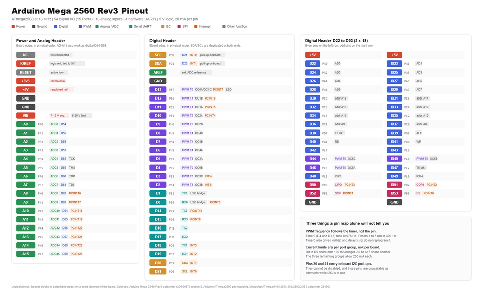
The full pin-by-pin table for all 100 package pins is published in Arduino's ATmega2560 pin mapping reference. 3
Pins That Are Not Broken Out
Sixteen of the chip's I/O lines never reach a header: PE2, PE6, PE7, PH2, PH7, PG3, PG4, PD4, PD5, PD6, and PJ2 through PJ7.
That costs you real capability. INT6 and INT7 exist on PE6 and PE7, but you cannot reach them, which is why the Mega has six usable external interrupts rather than eight. You also lose ICP1 on PD4 and the USART1 external clock on PD5. If you need those, you are designing your own board around the ATmega2560, not using a Mega.
Arduino Mega 2560 vs Arduino Uno: The Pinout Differences That Break Code
An Uno sketch will usually compile for a Mega without complaint and then fail at runtime, because the peripherals moved.
Function | Arduino Uno R3 | Arduino Mega 2560 | Migration impact |
Digital I/O | 14 | 54 | None |
Analog inputs | 6 | 16 | None |
Hardware UARTs | 1 | 4 | You can drop SoftwareSerial |
I2C | A4 (SDA), A5 (SCL) | D20 (SDA), D21 (SCL) | Rewire, and Uno shields need jumpers11 |
SPI | D10 to D13 | D50 to D53 | Rewire, or use the ICSP header10 |
Timer0 PWM pins | D5, D6 | D4, D13 | Frequency-sensitive code moves |
External interrupts | D2, D3 | D2, D3, D18 to D21 | Superset, no breakage |
Flash / SRAM | 32 KB / 2 KB | 256 KB / 8 KB | Room for much larger sketches |
The I2C move is the one that catches people out most, because an Uno shield with I2C hardwired to A4 and A5 will sit on a Mega making no electrical connection to the bus at all. The board looks seated, the sketch runs, and every transaction times out.
Recommended Reading: Arduino UNO Pinout: Comprehensive Guide for Engineers and Students
What Shield Compatibility Actually Covers
Arduino designed the Mega 2560 headers to stay mechanically compatible with the Uno and the older Duemilanove and Diecimila boards. Digital pins 0 to 13 with the adjacent AREF and GND pins, analog inputs 0 to 5, the power header, and the ICSP header all sit in equivalent locations.6
The functional overlap goes further than the physical layout. The main UART is on the same pins 0 and 1, and external interrupts 0 and 1 remain on pins 2 and 3.
The exception is the one above. Arduino states plainly that I2C is not on the same pins on the Mega 2560 (20 and 21) as on the Duemilanove and Diecimila (analog inputs 4 and 5). A shield is compatible right up until it tries to talk I2C.
If you are unsure whether a specific shield will work, the reliable check is the board schematic rather than the pin labels. Trace which header pins the shield actually drives and compare them against the reference table above.
Common Pinout Mistakes and Troubleshooting
Your sketch will not upload after wiring something to D0 or D1. Those pins are shared with the ATmega16U2 USB bridge. Disconnect anything on them before uploading.
A shield's I2C or SPI does nothing. Check whether the shield was designed for the Uno. I2C at A4/A5 and SPI at D10 to D13 both land on live pins, but are wired to something else.
Hardware SPI has stopped working. Confirm D53 is set as an output. As an input pulled low, it forces the SPI peripheral out of controller mode.
Analog readings drift or read full scale. Check the AREF pin. If you selected an internal reference in software while a voltage is applied to AREF, you have created a conflict at the reference node.
LEDs are dim, or the output sags under load. Add up the current per port group, not per pin. Pins D0 to D5 share a 100 mA budget, and A0 to A15 share another.
PWM changed frequency on a pin you did not touch. You reconfigured a timer that drives more than one pin. Consult the timer map above before changing any prescaler.9
The millis() clock stopped advancing. Something reprogrammed Timer0. Move your PWM output to a Timer3, Timer4, or Timer5 pin.13
Conclusion
The Arduino Mega 2560 pinout gives you 54 digital pins, 16 analog inputs, and four UARTs, but the useful mental model is not a list of pins. It is a map of which pins share a timer, which share a current budget, and which are already committed to a peripheral.
Before you commit a design, resolve the conflicts in that order: assign the fixed-function pins first (SPI, I2C, and the UARTs you need), then the six external interrupts, then PWM by timer group, and finally the plain digital I/O. Check your current totals against the port groups rather than the per-pin rating.
Do that, and the Mega's pin count becomes the advantage it is meant to be, rather than 54 opportunities to discover a shared peripheral the hard way.
Frequently Asked Questions
How many pins does the Arduino Mega 2560 have?
The Arduino Mega 2560 has 70 usable I/O pins: 54 digital and 16 analog. The underlying ATmega2560 chip has 86 general-purpose I/O lines in a 100-pin package, so 16 of them are not brought out to headers.
Which pins are PWM on the Arduino Mega 2560?
Fifteen pins support analogWrite() on the Arduino Mega 2560: D2 through D13, plus D44, D45, and D46. They are marked with a tilde on the silkscreen. Pins 4 and 13 run at roughly 976 Hz, and the other 13 run at roughly 490 Hz.8
Which pins are I2C on the Arduino Mega 2560?
On the Arduino Mega 2560, I2C runs on D20 (SDA) and D21 (SCL), both of which are duplicated on the dedicated SDA and SCL pins beside AREF. This differs from the Uno, which uses A4 and A5 for I2C. The Mega also has onboard pull-ups on pins 20 and 21.11
Which pins are SPI on the Arduino Mega 2560?
On the Arduino Mega 2560, SPI runs on D50 (CIPO/MISO), D51 (COPI/MOSI), D52 (SCK), and D53 (CS/SS). The same signals are also available on the ICSP header, which is why Uno shields that use the ICSP header remain compatible with the Mega.10
How much current can an Arduino Mega 2560 pin supply?
Arduino specifies 20 mA maximum per I/O pin. The ATmega2560 absolute maximum rating is 40 mA, but that is a stress limit and not a design target. Port groups are also capped at 100 mA or 200 mA in total.
Can I use analog pins as digital pins on the Mega 2560?
Yes. A0 to A15 work as ordinary digital I/O, and they also carry the digital aliases D54 to D69. They share a 100 mA group budget with each other.
Which Arduino Mega 2560 pins support interrupts?
Pins 2, 3, 18, 19, 20, and 21 support external interrupts. Pins 20 and 21 are unavailable for interrupts while in use for I2C. A further 19 pin change interrupts are available on ports B, J, K, and pin D0.7
Why does my Arduino Uno shield not work on the Mega 2560?
Because I2C and SPI sit on different pins. Uno shields expect I2C on A4 and A5 and SPI on pins 10 to 13, and neither lands on the corresponding bus on a Mega. Shields taking SPI from the ICSP header are unaffected.
What is the IOREF pin for?
IOREF tells a shield what logic voltage the board runs at, so a shield can adapt its level shifting. On the Mega 2560, it is connected to the 5 V rail.
References
[1] Arduino, "Arduino Mega 2560 Rev3 Datasheet (A000067)," Arduino. [Online]. Available: https://docs.arduino.cc/resources/datasheets/A000067-datasheet.pdf
[2] Arduino, "Arduino Mega 2560 Rev3 Product Page and Tech Specs," Arduino. [Online]. Available: https://store-usa.arduino.cc/products/arduino-mega-2560-rev3
[3] Arduino, "Arduino Mega 2560 Rev3 Full Pinout Diagram," Arduino. [Online]. Available: https://docs.arduino.cc/resources/pinouts/A000067-full-pinout.pdf
[4] Microchip Technology, "ATmega640/1280/1281/2560/2561 Datasheet (2549Q-AVR-02/2014)," Microchip Technology. [Online]. Available: https://ww1.microchip.com/downloads/en/devicedoc/atmel-2549-8-bit-avr-microcontroller-atmega640-1280-1281-2560-2561_datasheet.pdf
[5] Arduino, "ATmega2560-Arduino Pin Mapping," Arduino. [Online]. Available: https://docs.arduino.cc/retired/hacking/hardware/PinMapping2560/
[6] Arduino, "Mega 2560 Rev3 Product Documentation," Arduino. [Online]. Available: https://docs.arduino.cc/hardware/mega-2560/
[7] Arduino, "attachInterrupt() Language Reference," Arduino. [Online]. Available: https://docs.arduino.cc/language-reference/en/functions/external-interrupts/attachInterrupt/
[8] Arduino, "analogWrite() Language Reference," Arduino. [Online]. Available: https://docs.arduino.cc/language-reference/en/functions/analog-io/analogWrite/
[9] Arduino, "Basics of PWM (Pulse Width Modulation)," Arduino. [Online]. Available: https://docs.arduino.cc/learn/microcontrollers/analog-output/
[10] Arduino, "SPI Library Reference," Arduino. [Online]. Available: https://docs.arduino.cc/language-reference/en/functions/communication/SPI/
[11] Arduino, "Wire (I2C) Library Reference," Arduino. [Online]. Available: https://docs.arduino.cc/language-reference/en/functions/communication/wire/
[12] Arduino, "ArduinoCore-avr: boards.txt," GitHub. [Online]. Available: https://github.com/arduino/ArduinoCore-avr/blob/master/boards.txt
[13] Arduino, "ArduinoCore-avr: cores/arduino/wiring.c," GitHub. [Online]. Available: https://github.com/arduino/ArduinoCore-avr/blob/master/cores/arduino/wiring.c
[14] Arduino, "ArduinoCore-avr," GitHub. [Online]. Available: https://github.com/arduino/ArduinoCore-avr
in this article
1. Key Takeaways2. Introduction3. Arduino Mega 2560 Specifications 4. Complete Arduino Mega 2560 Pin Reference Table5. Power Pins and Electrical Limits6. Digital I/O Pins (D0 to D53)7. PWM Pins and the Timer Map8. Analog Input Pins (A0 to A15)9. Serial (UART) Pins: Four Hardware Ports10. I2C Pins: D20 (SDA) and D21 (SCL)11. SPI Pins: D50 to D53 and the ICSP Header12. External and Pin Change Interrupts13. ATmega2560 to Arduino Pin Mapping14. Arduino Mega 2560 vs Arduino Uno: The Pinout Differences That Break Code15. Common Pinout Mistakes and Troubleshooting16. Conclusion17. Frequently Asked Questions18. References