ATmega328P: Pinout, Registers, Fuses, and Arduino Pin Mapping
Complete ATmega328P reference: PDIP and QFN/MLF pinout, port registers, fuse bytes, Arduino pin mapping, errata, and lifecycle status.

05 Aug, 2026. 15 minutes read
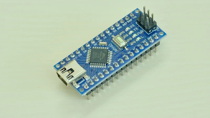
Arduino Nano powered by the ATmega328P
Key Takeaways
The ATmega328P is an 8-bit AVR microcontroller with 32 KB flash memory, 2 KB SRAM, 1 KB EEPROM, and 23 programmable I/O lines, rated to 20 MHz at 4.5 V to 5.5 V.
Package choice changes what you get: the 28-pin PDIP exposes 6 analog inputs, while the 32-pin TQFP and QFN/MLF expose 8 by adding ADC6 and ADC7.
Arduino PINs are a software abstraction. D0 to D13 and A0 to A5 map onto physical ports PB, PC, and PD, and knowing that mapping is what lets you use direct port manipulation.
Three fuse bytes control the clock source, brown-out level, bootloader size, and reset vector. Writing the wrong CKSEL bits is the single most common way to make a chip look dead.
Microchip lists the ATmega328P as "Not Recommended for new designs," so treat it as a prototyping and maintenance part rather than the basis of a new production run.
Introduction
The ATmega328P is an 8-bit AVR microcontroller from Microchip Technology with 32 KB of Flash memory, 2 KB of SRAM, and 1 KB of EEPROM. Best known as the chip behind the Arduino Uno and Arduino Nano, the ATmega328P remains one of the most widely used microcontrollers for embedded systems, prototyping, and education. Built on the AVR-enhanced RISC architecture, the ATmega328P delivers approximately 1 MIPS per MHz because most instructions execute in a single clock cycle [1].
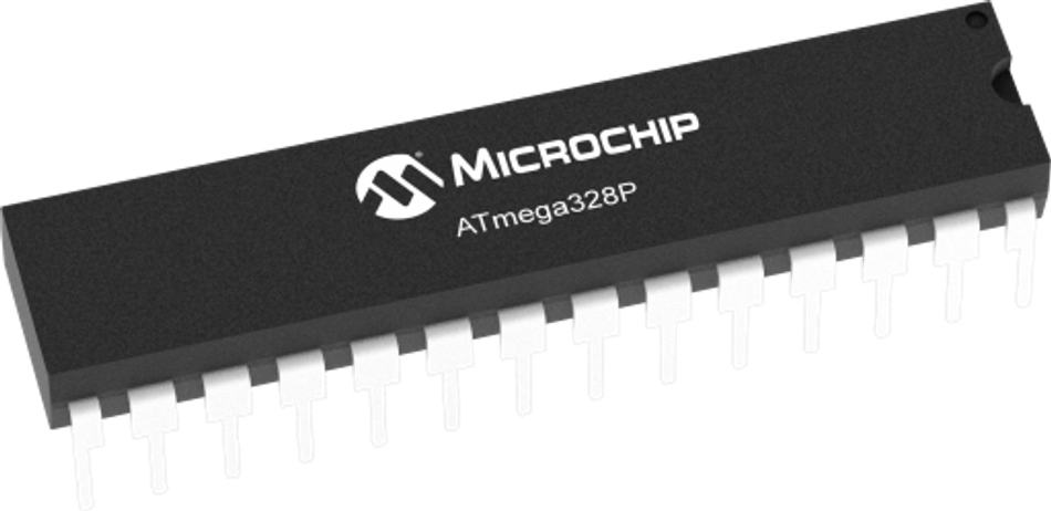
Whether you're using the ATmega328P through the Arduino ecosystem or designing a standalone embedded system, understanding its pinout, peripherals, registers, and fuse settings is essential. This guide explains the ATmega328P from both perspectives.
It is based on the official Microchip datasheet and Arduino pin mapping rather than secondary sources, so the specifications and pin assignments presented here are suitable for real-world hardware design
ATmega328P Specifications
Before getting into pinouts and registers, here's the quick-reference version: the numbers you'd actually compare against another chip when deciding whether the ATmega328P fits a design. The table below pulls these directly from Microchip's datasheet [1]
Parameter | Value |
Architecture | 8-bit AVR enhanced RISC |
Flash memory | 32 KB (in-system self-programmable) |
SRAM | 2 KB |
EEPROM | 1 KB |
General purpose working registers | 32 |
Programmable I/O lines | 23 |
Max CPU speed | 20 MHz at 4.5 V to 5.5 V |
Operating voltage | 1.8 V to 5.5 V |
Speed grades | 4 MHz at 1.8 V, 10 MHz at 2.7 V, 20 MHz at 4.5 V [1] |
ADC | 10-bit, 6 channels (PDIP) or 8 channels (TQFP/QFN-MLF) |
Timers | Two 8-bit, one 16-bit |
PWM channels | 6 |
Serial interfaces | USART, master/slave SPI, 2-wire (I2C compatible) |
Sleep modes | 6 |
Temperature range | -40 °C to 85 °C (standard grade) |
Packages | 28-pin PDIP, 28-pad QFN/MLF, 32-lead TQFP, 32-pad QFN/MLF |
Note the speed grade detail. The 20 MHz figure is only valid from 4.5 V upward. If you run the chip at 3.3 V, it's capped at around 10 MHz, which is why 3.3 V Arduino-compatible boards typically run at 8 MHz [1].
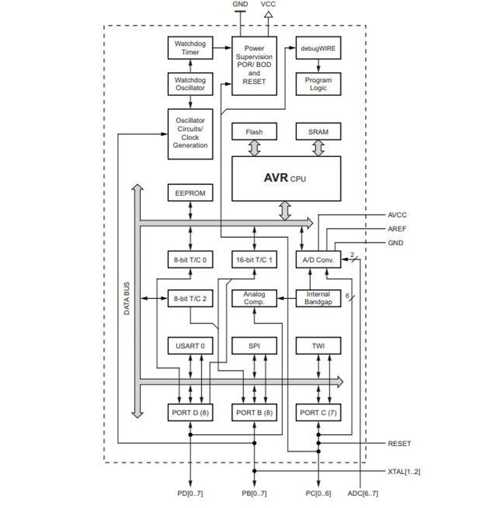
ATmega328P Pinout by Package
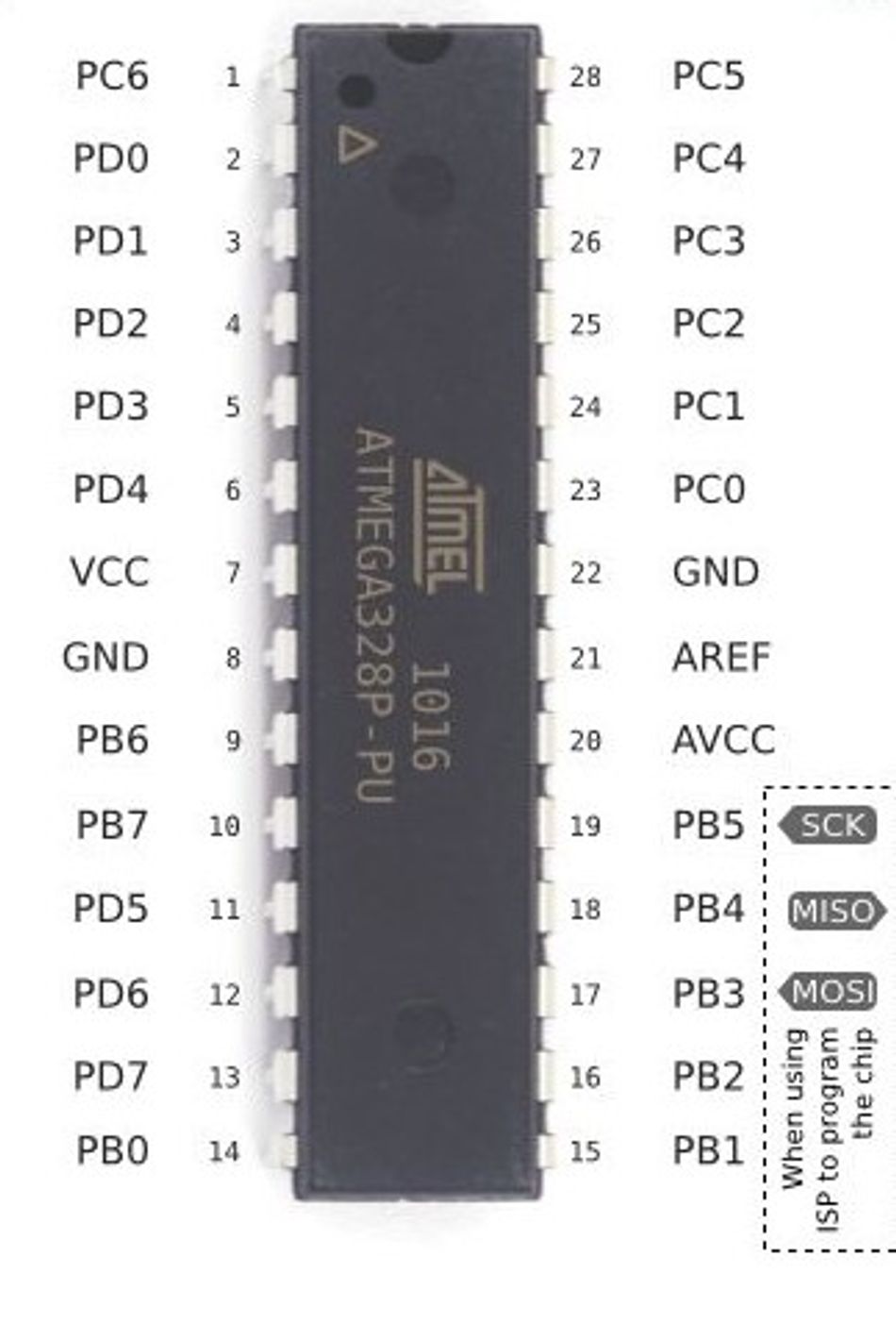
28-pin PDIP Pinout
This is the layout to know if you're building on a breadboard, working with an Arduino Uno directly, or designing a through-hole board; it's the most common package this chip ships in for hobbyist and prototyping work
Pin | AVR pin | Alternate functions |
1 | PC6 | RESET, PCINT14 |
2 | PD0 | RXD, PCINT16 |
3 | PD1 | TXD, PCINT17 |
4 | PD2 | INT0, PCINT18 |
5 | PD3 | OC2B, INT1, PCINT19 |
6 | PD4 | XCK, T0, PCINT20 |
7 | VCC | Digital supply |
8 | GND | Ground |
9 | PB6 | XTAL1, TOSC1, PCINT6 |
10 | PB7 | XTAL2, TOSC2, PCINT7 |
11 | PD5 | OC0B, T1, PCINT21 |
12 | PD6 | OC0A, AIN0, PCINT22 |
13 | PD7 | AIN1, PCINT23 |
14 | PB0 | CLKO, ICP1, PCINT0 |
15 | PB1 | OC1A, PCINT1 |
16 | PB2 | SS, OC1B, PCINT2 |
17 | PB3 | MOSI, OC2A, PCINT3 |
18 | PB4 | MISO, PCINT4 |
19 | PB5 | SCK, PCINT5 |
20 | AVCC | ADC supply |
21 | AREF | ADC reference |
22 | GND | Ground |
23 | PC0 | ADC0, PCINT8 |
24 | PC1 | ADC1, PCINT9 |
25 | PC2 | ADC2, PCINT10 |
26 | PC3 | ADC3, PCINT11 |
27 | PC4 | ADC4, SDA, PCINT12 |
28 | PC5 | ADC5, SCL, PCINT13 |
A note on pin 1 (PC6): This pin only acts as RESET when the RSTDISBL fuse is left unprogrammed, which is the factory default. If RSTDISBL is programmed, PC6 becomes a regular I/O pin instead and external reset stops working; a common source of "why won't my chip reset" confusion when someone has reused a fuse configuration from another project.
28-pin QFN/MLF Pinout
If you're moving from breadboard to a compact PCB layout, this is the pinout you'll actually route; same electrical behavior as the PDIP, just a different physical arrangement suited to reflow soldering.
QFN/MLF Pin | AVR Pin | Alternate Functions |
1 | PD3 | OC2B, INT1, PCINT19 |
2 | PD4 | XCK, T0, PCINT20 |
3 | VCC | Digital supply |
4 | GND | Ground |
5 | PB6 | XTAL1, TOSC1, PCINT6 |
6 | PB7 | XTAL2, TOSC2, PCINT7 |
7 | PD5 | OC0B, T1, PCINT21 |
8 | PD6 | OC0A, AIN0, PCINT22 |
9 | PD7 | AIN1, PCINT23 |
10 | PB0 | CLKO, ICP1, PCINT0 |
11 | PB1 | OC1A, PCINT1 |
12 | PB2 | SS, OC1B, PCINT2 |
13 | PB3 | MOSI, OC2A, PCINT3 |
14 | PB4 | MISO, PCINT4 |
15 | PB5 | SCK, PCINT5 |
16 | AVCC | ADC supply |
17 | AREF | ADC reference |
18 | GND | Ground |
19 | PC0 | ADC0, PCINT8 |
20 | PC1 | ADC1, PCINT9 |
21 | PC2 | ADC2, PCINT10 |
22 | PC3 | ADC3, PCINT11 |
23 | PC4 | ADC4, SDA, PCINT12 |
24 | PC5 | ADC5, SCL, PCINT13 |
25 | PC6 | RESET, PCINT14 |
26 | PD0 | RXD, PCINT16 |
27 | PD1 | TXD, PCINT17 |
28 | PD2 | INT0, PCINT18 |
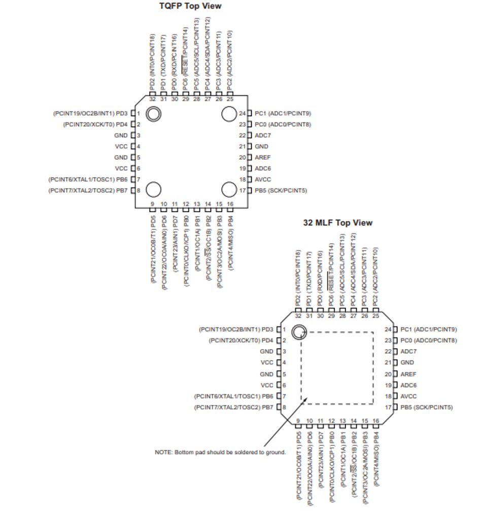
32-pin TQFP and QFN/MLF Pinout
The surface mount packages raise the pin count to 32 and expose two extra analog inputs, ADC6 and ADC7. These two are analog only. They have no digital port register behind them, so you can read them with the ADC, but you cannot use them as GPIO.
The TQFP layout also splits VCC and GND across two pairs of pins instead of one. If you are laying out a board, decouple both. Reach for this package when a design needs those two extra analog channels, or when board space favors a smaller surface-mount footprint over the 28-pin part.
Same pin numbering for both packages.
Pin | AVR Pin | Alternate Functions |
1 | PD3 | OC2B, INT1, PCINT19 |
2 | PD4 | XCK, T0, PCINT20 |
3 | GND | Ground |
4 | VCC | Digital supply |
5 | GND | Ground |
6 | VCC | Digital supply |
7 | PB6 | XTAL1, TOSC1, PCINT6 |
8 | PB7 | XTAL2, TOSC2, PCINT7 |
9 | PD5 | OC0B, T1, PCINT21 |
10 | PD6 | OC0A, AIN0, PCINT22 |
11 | PD7 | AIN1, PCINT23 |
12 | PB0 | CLKO, ICP1, PCINT0 |
13 | PB1 | OC1A, PCINT1 |
14 | PB2 | SS, OC1B, PCINT2 |
15 | PB3 | MOSI, OC2A, PCINT3 |
16 | PB4 | MISO, PCINT4 |
17 | PB5 | SCK, PCINT5 |
18 | AVCC | ADC supply |
19 | ADC6 | Analog input only, no port register |
20 | AREF | ADC reference |
21 | GND | Ground |
22 | ADC7 | Analog input only, no port register |
23 | PC0 | ADC0, PCINT8 |
24 | PC1 | ADC1, PCINT9 |
25 | PC2 | ADC2, PCINT10 |
26 | PC3 | ADC3, PCINT11 |
27 | PC4 | ADC4, SDA, PCINT12 |
28 | PC5 | ADC5, SCL, PCINT13 |
29 | PC6 | RESET, PCINT14 |
30 | PD0 | RXD, PCINT16 |
31 | PD1 | TXD, PCINT17 |
32 | PD2 | INT0, PCINT18 |
Power and Reference Pins
AVCC is the supply for the A/D converter, for PC3 to PC0, and for ADC7 and ADC6. Connect it to VCC even when you do not use the ADC, and route it through a low-pass filter when you do.
AREF is the analog reference input. PC6 to PC4 run from the digital VCC rather than AVCC, which matters if you are partitioning analog and digital supplies.
Ports and Registers: How AVR I/O Works
DDRx, PORTx, and PINx
Every I/O port on the ATmega328P is controlled by three registers, where x is B, C, or D:
DDRx sets direction. A 1 makes the pin an output, a 0 makes it an input.
PORTx sets the output level when the pin is an output. When the pin is an input, writing a 1 enables the internal pull-up resistor.
PINx reads the actual logic level at the pin. Writing a 1 to a PINx bit toggles the corresponding PORTx bit.
This is what pinMode() and digitalWrite() compile down to. Writing the registers directly is faster because you can change eight pins in one instruction instead of looping.
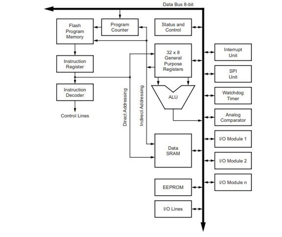
Port B and Port D are 8-bit. Port C is 7-bit, and its top pin, PC6, is the reset pin unless you reprogram a fuse.
Alternate Pin Functions
Almost every pin carries a peripheral function alongside its GPIO role. Enabling the peripheral overrides the port register for that pin.
The groupings worth memorising:
SPI sits on PB2 to PB5: SS, MOSI, MISO, and SCK respectively.
USART sits on PD0 (RXD) and PD1 (TXD).
I2C sits on PC4 (SDA) and PC5 (SCL).
Crystal oscillator pins are PB6 (XTAL1) and PB7 (XTAL2).
External interrupts INT0 and INT1 are PD2 and PD3, and pin change interrupts (PCINT0 to PCINT23, with PCINT15 unused) cover every I/O pin.
That last point is useful. If you need more than two edge-triggered interrupts, pin change interrupts give you coverage on all 23 lines, at the cost of having to work out which pin in the group changed.
Arduino Pin Mapping: From Chip Pins to D0-D13 and A0-A5
Arduino renames the ports into a flat numbering scheme. The official Arduino ATmega328P pin mapping document details the correspondence, and note that it specifically describes the DIP package [5].
Arduino pin | AVR pin | PDIP pin | Notes |
D0 | PD0 | 2 | Serial RX |
D1 | PD1 | 3 | Serial TX |
D2 | PD2 | 4 | INT0 |
D3 | PD3 | 5 | PWM, INT1 |
D4 | PD4 | 6 | General purpose |
D5 | PD5 | 11 | PWM |
D6 | PD6 | 12 | PWM |
D7 | PD7 | 13 | General purpose |
D8 | PB0 | 14 | Input capture |
D9 | PB1 | 15 | PWM |
D10 | PB2 | 16 | PWM, SPI SS |
D11 | PB3 | 17 | PWM, MOSI |
D12 | PB4 | 18 | MISO |
D13 | PB5 | 19 | SCK, onboard LED |
A0 to A5 | PC0 to PC5 | 23 to 28 | A4 is SDA, A5 is SCL |
ATmega328P 28-Pin DIP to Arduino Uno pin mapping.
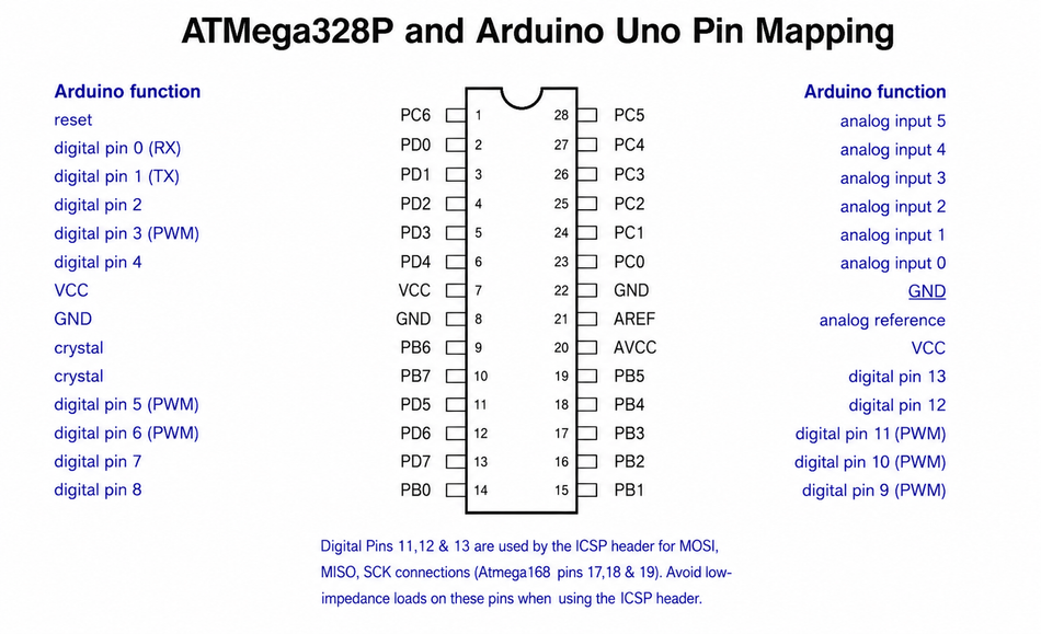
Two consequences follow from this table.
The six PWM pins on Arduino boards (3, 5, 6, 9, 10, 11) are not arbitrary. They are the six output compare pins of the three timers, which is why pins sharing a timer also share a PWM frequency and why changing one timer's prescaler affects both of its pins [5].
D13 is also SCK. The onboard LED sits on the SPI clock line, so the LED flickers during SPI traffic and an LED with a low value series resistor can load the bus.
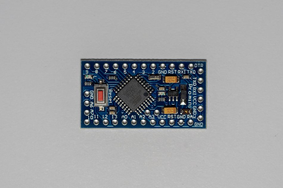
As the ATmega168/328P mapping reference notes, the Arduino Mini uses a smaller physical package that adds the two extra ADC pins, which the DIP-based boards do not expose [6].
Recommended Reading: Arduino UNO Pinout: Comprehensive Guide for Engineers and Students
Clock Sources and the Fuse Bits That Select Them
The Three Fuse Bytes
Fuses are configuration bits held outside the flash memory. They are read as logical zero when programmed, which reverses the intuition of most engineers the first time they meet them.
The ATmega328P has three fuse bytes. Getting these three bytes wrong is the single most common reason a 'dead' ATmega328P isn't actually dead; it's just configured to expect a clock source, reset behavior, or programming interface that isn't what you think it is. Here's what each byte actually controls
Fuse byte | Key bits | Controls |
Low | CKSEL3:0, SUT1:0, CKDIV8, CKOUT | Clock source, startup time, divide-by-8 prescaler |
High | RSTDISBL, DWEN, SPIEN, WDTON, EESAVE, BOOTSZ1:0, BOOTRST | Reset pin, debugWIRE, SPI programming, watchdog timer, EEPROM preservation, bootloader size and reset vector |
Extended | BODLEVEL2:0 | Brown-out detector trigger level |
By default SPIEN is programmed, which is what keeps in-system programming available. WDTON, RSTDISBL, and DWEN ship unprogrammed.
Note that only the low three bits of the extended fuse byte are implemented on this device. That is why you will see the same brown-out setting written as either 0x05 or 0xFD in different toolchains. Both program BODLEVEL to the same value, and the unimplemented upper bits read back as 1.
Arduino Uno and Nano Fuse Values
The Arduino AVR core's boards.txt file records the exact fuse values burned into each board's bootloader, and comparing the Uno's numbers against the Nano's is the fastest way to understand why the two boards, despite running the same chip at the same clock speed, don't offer quite the same amount of usable flash. The difference isn't the silicon; it's how each board's manufacturer configured the bootloader that ships pre-installed on it. A larger bootloader reserves more flash for itself, leaving less room for your actual sketch. The table below lays out precisely which fuse bytes differ, and by how much, for the two most common boards built on this chip
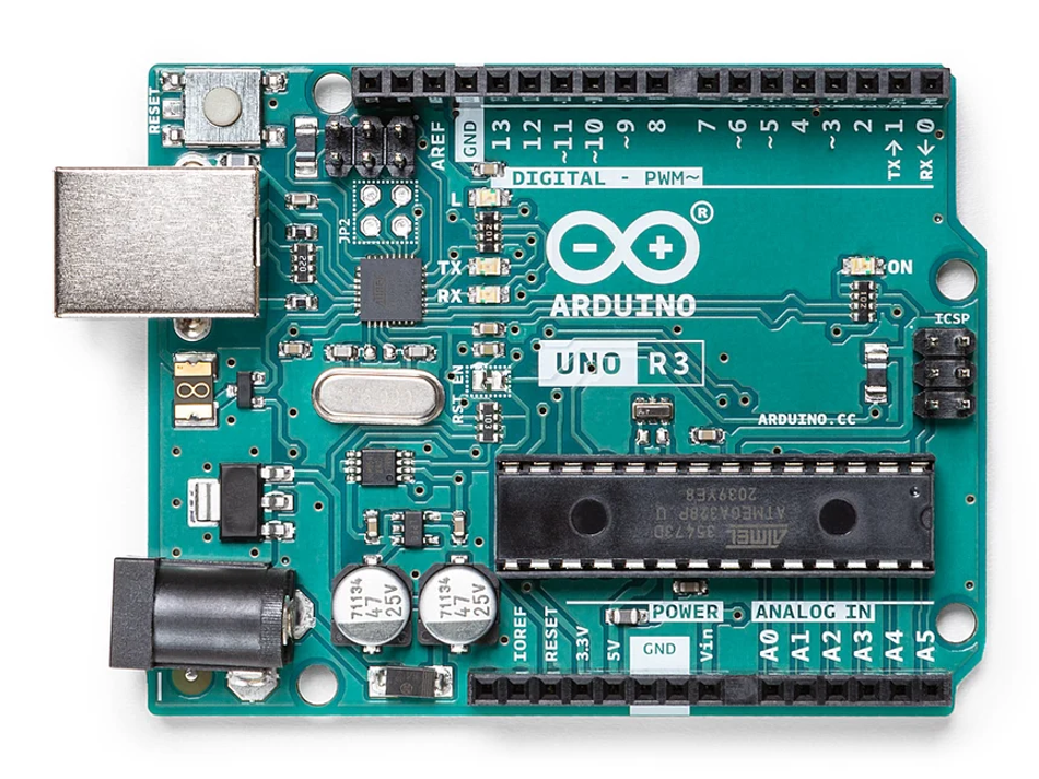
Arduino Uno Rev3
Setting | Arduino Uno | Arduino Nano (ATmega328P) |
Low fuse | 0xFF | 0xFF |
High fuse | 0xDE | 0xDA |
Extended fuse | 0xFD | 0xFD |
Bootloader Boot section size | Optiboot 512 bytes | Optiboot 2 KB |
Max sketch size | 32,256 bytes | 30,720 bytes |
Max SRAM | 2,048 bytes | 2,048 bytes |
CPU speed | 16 MHz | 16 MHz |
The only difference is the high fuse, and specifically the BOOTSZ bits. The Uno reserves 512 bytes for the bootloader, the Nano reserves 2 KB, and that 1,536-byte gap is exactly the difference in available flash memory.
Note: The Tools > Processor selection matters here. A default Nano uses the values above (Optiboot, 0xDA, 30,720 bytes) [7]. Selecting "ATmega328P (Old Bootloader)" from that menu keeps the same fuse and size values but swaps in the older ATmegaBOOT bootloader instead of Optiboot.
Suggested Reading: Selecting a microcontroller (MCU) for your IoT product
Choosing a Clock Source
The chip ships running from its calibrated internal RC oscillator at 8 MHz with the CKDIV8 fuse programmed, so a factory-fresh part actually runs at 1 MHz.
The internal oscillator is factory calibrated to within ±10% at 3 V and 25 °C. User calibration tightens that to ±1% over 1.8 V to 5.5 V and -40 °C to 85 °C.
That ±10% figure is the reason you should not run asynchronous serial from the uncalibrated internal oscillator. UART framing tolerates roughly 2% total clock error between two devices, so a 10% deviation guarantees corrupted bytes. Fit an external crystal oscillator when the design depends on USART timing.
Memory Map: Flash, SRAM, EEPROM
The ATmega328P splits storage three ways, and the split matters because each has a different lifetime and access cost.
Flash memory holds your program: 32 KB, organised for read-while-write so a bootloader in the boot section can rewrite the application section while still executing.
SRAM holds variables at runtime: 2 KB, which is the constraint you hit first in practice. A single 1 KB buffer consumes half of it, and stack overflow on AVR fails silently by corrupting variables rather than trapping.
EEPROM holds 1 KB of data that survives power loss, for calibration constants and settings. The EESAVE fuse decides whether a chip erase wipes it.
Within the ATmega328 family, the only differences are memory size, bootloader support, and interrupt vector size; within each size, the picoPower power-management features distinguish the "PA" (or 328P) variant from its plain counterpart. The ATmega328 and ATmega328P both carry 32 KB flash, 1 KB EEPROM, 2 KB SRAM, and 2-instruction-word interrupt vectors.
Peripherals: Timers, PWM, ADC, and Serial
Timers and PWM
Three timer/counters are available: Timer0 and Timer2 are 8-bit, Timer1 is 16-bit. Each supports compare mode, and Timer1 adds an input capture unit on PB0 for measuring pulse widths precisely.
Together they provide six PWM channels. Timer2 also runs asynchronously from a 32 kHz crystal on TOSC1 and TOSC2, which is how you build a real-time counter that keeps running while the CPU sleeps.
Analog Inputs
The ADC is 10-bit with a sample-and-hold. You get 6 analog inputs in the PDIP package and 8 in the TQFP and QFN/MLF packages, plus an internal temperature sensor channel.
There is a dedicated ADC noise reduction sleep mode that halts the CPU and most I/O during a conversion. If you need clean readings near the bottom of the range, use it, and filter AVCC properly.
USART, SPI, and I2C
The chip carries one programmable USART, one master/slave SPI port, and one byte-oriented 2-wire interface that is I2C compatible.
SPI uses MOSI, MISO, SCK, and SS on Port B, and doubles as the in-system programming interface. That overlap is deliberate, and it is also why an SPI peripheral wired to those pins can interfere with programming if it drives the bus during reset. For a deeper treatment, link internally to an SPI protocol explainer and an I2C explainer.
Recommended Reading: I2C vs SPI vs UART: A Comprehensive Comparison
Power-Saving Modes and Current Consumption
The ATmega offers six sleep modes: idle, ADC noise reduction, power-save, power-down, standby, and extended standby. They differ in which clock domains keep running.
These numbers matter most if you're designing something battery-powered: a coin-cell sensor node, for example, where the difference between microamps and milliamps decides whether the device lasts weeks or years. Measured supply current for the ATmega328P, from the datasheet:
Mode | Condition | Typical |
Active | 1 MHz, 2 V | 0.3 mA |
Active | 4 MHz, 3 V | 1.7 mA |
Active | 8 MHz, 5 V | 5.2 mA |
Idle | 1 MHz, 2 V | 0.04 mA |
Idle | 8 MHz, 5 V | 1.2 mA |
Power-save | 32 kHz oscillator on, 1.8 V | 0.8 µA |
Power-down | Watchdog timer on, 3 V | 4.2 µA |
Power-down | Watchdog timer off, 3 V | 0.1 µA |
The jump from 4.2 µA to 0.1 µA is the whole battery-life conversation in one row. If a coin cell design is missing its target, check whether the watchdog timer is still enabled in power-down [1].
ATmega328P vs ATmega328 vs ATmega328PB
These three parts are frequently confused, and the differences are real enough to break a build. Microchip's application note AT15007 documents the ATmega328PB changes in full. The short version: the 328P is a lower-power revision of the plain 328, and the 328PB is a separate, more capable chip with extra peripherals; not simply a newer version of the 328P.
Feature | ATmega328 | ATmega328P | ATmega328PB |
Flash, SRAM, EEPROM | 32 KB, 2 KB, 1 KB | 32 KB, 2 KB, 1 KB | 32 KB, 2 KB, 1 KB |
picoPower | No | Yes | Yes |
USART | 1 | 1 | 2 |
SPI | 1 | 1 | 2 |
I2C (TWI) | 1 | 1 | 2 |
16-bit timers | 1 | 1 | 3 |
PWM channels | 6 | 6 | 10 |
Full swing crystal oscillator | Yes | Yes | No |
Internal RC accuracy (factory) | ±10% | ±10% | ±2% [2] |
Peripheral Touch Controller | No | No | Yes |
Clock failure detection | No | No | Yes |
Signature bytes | 0x1E 0x95 0x14 | 0x1E 0x95 0x0F | 0x1E 0x95 0x16 |
The signature bytes are the practical detail. Toolchains identify the part from those three bytes, so an ATmega328 will not accept a binary targeted at an ATmega328P without a configuration change, even though the silicon is otherwise near identical.
The ATmega328PB is not a drop-in replacement. It adds four GPIOs on Port E, and on the 32-pin package it repurposes pin 3 (GND) and pin 6 (VCC) as PE0 and PE1. Dropping a 328PB into a board laid out for a 328P therefore connects two supply rails to general-purpose I/O [2].
The 328PB also removes the full-swing crystal oscillator option and consumes more current in power-save mode, so it is an upgrade on peripheral count rather than a strict improvement.
Silicon Errata You Should Know
Microchip publishes silicon errata separately from the datasheet, and one item applies to every revision of the ATmega328/P shipped.
Analog comparator multiplexer. If you set the ACME bit in ADCSRB while MUX3 in ADMUX is 1, all multiplexers switch off until you clear ACME again. The workaround is to clear MUX3 before setting ACME. This affects revisions A, B, and D, meaning all of them.
TWI data setup time. Running as an I2C slave above 2 MHz system clock, the data setup time for the first bit after ACK can be too short and produce a false start or stop condition. Insert a delay between writing TWDR and TWCR. This one affects revision D.
32 kHz oscillator. On revisions A and B, the 32 kHz oscillator does not work as a system clock and is inaccurate as an asynchronous timer source. There is no workaround, so a real-time counter design should specify revision D silicon [4].
Lifecycle Status: Not Recommended for New Designs
Microchip currently lists the ATmega328P product status as "Not Recommended for new designs."
That does not mean unavailable. Microchip still quotes and stocks the range, with 5,000-unit pricing around 1.93 to 2.20 US dollars for standard temperature parts, and roughly 4.09 dollars for the -40°C to 125°C automotive grade versions. You can find distributors and more details on Findchips. [2].
Not every ATmega328P is the same physical part; package, temperature rating, and automotive qualification all show up as different order codes with different prices, so here's how to tell them apart when you're actually placing an order.
Part number | Package | Pins | Temperature range |
ATMEGA328P-PU | PDIP | 28 | -40 °C to 85 °C |
ATMEGA328P-PN | PDIP | 28 | -40 °C to 105 °C |
ATMEGA328P-AU | TQFP | 32 | -40 °C to 85 °C |
ATMEGA328P-AN | TQFP | 32 | -40 °C to 105 °C |
ATMEGA328P-MU | QFN/MLF | 32 | -40 °C to 85 °C |
ATMEGA328P-15AZ | TQFP | 32 | -40 °C to 125 °C |
What the status should change is your planning horizon. For prototyping, education, robotics coursework, and maintaining existing products, the part is fine and well supported. For a new design entering volume production, however, it is worth considering MCUs with a longer guaranteed lifecycle. Depending on your application requirements, suitable alternatives include newer AVR devices such as the AVR DA or AVR DB series, PIC microcontrollers, or ARM Cortex-M-based MCUs from vendors such as Texas Instruments, STMicroelectronics, or NXP.
Common Mistakes and Troubleshooting
The chip is dead after setting fuses. Almost always a CKSEL problem. If you select an external crystal oscillator and no crystal is fitted, the chip has no clock, and in-system programming needs a clock to respond. Feed a 1 MHz signal into XTAL1 to recover it, or use a high-voltage parallel programmer.
Programming stopped working entirely. Check whether you cleared SPIEN or programmed RSTDISBL. Disabling serial programming or turning the reset pin into GPIO both lock out the ISP interface, and recovery needs high-voltage programming.
Sketches upload but behave as if the clock is wrong. The CKDIV8 fuse divides the system clock by eight. A part running from the internal oscillator with CKDIV8 programmed runs at 1 MHz, not 8 MHz, and every delay is eight times too long.
Serial output is garbage. Either a baud rate mismatch or the internal oscillator tolerance problem described above. Confirm the actual CPU speed before blaming the code.
An output pin cannot drive the load. The 40 mA figure in the datasheet is an absolute maximum rating, not a design target. Absolute maximums are stress limits, and the total for all VCC and GND pins is 200 mA. Size drivers well below those numbers and use a transistor or MOSFET for anything substantial.
Analog readings are noisy. Confirm AVCC is connected and filtered, confirm AREF is configured to match the code, and try the ADC noise reduction sleep mode during conversions.
Conclusion
The ATmega328P earned its position by being predictable. A well-documented 8-bit AVR microcontroller with 32 KB flash memory, a clean three-register I/O model, and a peripheral set that covers most small embedded jobs.
Working with it effectively comes down to a few things the Arduino IDE abstracts away: knowing which physical pin a sketch pin maps to, knowing that fuses decide the clock before your code ever runs, and knowing that package choice changes your analog input count.
The ATmega328P is no longer recommended for new designs, but that doesn't mean it's obsolete. It's still a reliable choice for prototyping, education, robotics projects, and maintaining existing products. If you're developing a product for long-term or high-volume production, it's worth selecting a microcontroller with a longer guaranteed lifecycle.
Frequently Asked Questions
Is the ATmega328P the same as the ATmega328?
No. They share memory size and pinout, but the ATmega328P adds picoPower technology for lower power consumption, and the two report different signature bytes (0x1E 0x95 0x0F versus 0x1E 0x95 0x14), so toolchains treat them as separate devices.
How many pins does the ATmega328P have?
Pin count depends on package: 28 in the PDIP and 28-pad QFN/MLF, and 32 in the TQFP and 32-pad QFN/MLF. In every package, 23 of those are programmable I/O lines.
What is the maximum CPU speed?
20 MHz, but only at 4.5 V to 5.5 V. At 2.7 V the limit is 10 MHz, and at 1.8 V it is 4 MHz. Arduino boards run at 16 MHz.
Can the ATmega328P run without an external crystal?
Yes. It has a calibrated internal RC oscillator at 8 MHz, which is how minimal designs drop the crystal and its two load capacitors. Accept the ±10% accuracy limitation; avoid it for applications requiring accurate baud rates unless the oscillator error is acceptable.
How much of the 32 KB flash can a sketch actually use?
On an Arduino Uno, 32,256 bytes, because Optiboot occupies 512 bytes. On a Nano with the 2 KB bootloader, 30,720 bytes.
Why does the ATmega328P have 6 analog inputs on Arduino but the datasheet says 8?
The extra two channels, ADC6 and ADC7, exist only in the TQFP and QFN/MLF packages. The Arduino Uno uses the PDIP part, which does not bring them out.
Is the ATmega328P still in production?
It is still available to order from Microchip, but the product status is "Not Recommended for new designs." Use it for prototyping and existing products, and pick a current part for new volume designs.
What are the SPI pins on the ATmega328P?
PB2 is SS, PB3 is MOSI, PB4 is MISO, and PB5 is SCK, which correspond to Arduino pins D10 through D13.
References
[1] Microchip Technology Inc., ATmega48A/PA/88A/PA/168A/PA/328/P Data Sheet Complete, DS40002061A. [Online]. Available: https://www.microchip.com/en-us/product/ATmega328P. [Accessed: Aug. 4, 2026].
[2] Microchip Technology Inc., ATmega328P Product Page. [Online]. Available: https://www.microchip.com/en-us/product/ATmega328P [Accessed: Aug. 4, 2026].
[3] Microchip Technology Inc., AT15007: Differences between ATmega328/P and ATmega328PB (formerly Atmel-42559C, AN42559). [Online]. Available: https://onlinedocs.microchip.com/oxy/GUID-CBDC1838-0100-4F26-A45A-134958193C3B-en-US-4/index.html [Accessed: Aug. 4, 2026].
[4] Microchip Technology Inc., ATmega48A/PA/88A/PA/168A/PA/328/P Silicon Errata and Data Sheet Clarification, DS80000855A. [Online]. Available: https://ww1.microchip.com/downloads/en/DeviceDoc/ATmega48APA88APA168APA328P-SiliConErrataClarif-DS80000855A.pdf. [Accessed: Aug. 4, 2026].
[5] Arduino, ATmega328P Pin Mapping (pins_arduino.h). [Online]. Available: https://github.com/arduino/ArduinoCore-avr/blob/master/variants/standard/pins_arduino.h. [Accessed: Aug. 4, 2026].
[6] Arduino, ATmega168/328P Arduino Pin Mapping (Standard Variant). [Online]. Available: https://github.com/arduino/ArduinoCore-avr/tree/master/variants/standard. [Accessed: Aug. 4, 2026].
[7] Arduino, ArduinoCore-avr boards.txt. [Online]. Available: https://github.com/arduino/ArduinoCore-avr/blob/master/boards.txt [Accessed: Aug. 4, 2026].
<grammarly-extension-vbars></grammarly-extension-vbars>
in this article
1. Key Takeaways2. Introduction3. ATmega328P Specifications4. ATmega328P Pinout by Package5. Ports and Registers: How AVR I/O Works6. Arduino Pin Mapping: From Chip Pins to D0-D13 and A0-A57. Clock Sources and the Fuse Bits That Select Them8. Memory Map: Flash, SRAM, EEPROM9. Peripherals: Timers, PWM, ADC, and Serial10. Power-Saving Modes and Current Consumption11. ATmega328P vs ATmega328 vs ATmega328PB12. Silicon Errata You Should Know13. Lifecycle Status: Not Recommended for New Designs14. Common Mistakes and Troubleshooting15. Conclusion16. Frequently Asked Questions17. References