

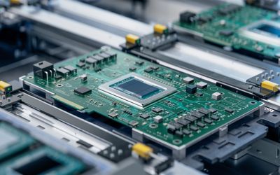
Long-term component reliability is a function of storage conditions, certification frameworks, and supply chain transparency.
Be the first to know.
Get our semiconductors weekly email digest.
Tagged with
semiconductors
ORGANIZATIONS. SHAPING THE INDUSTRY.

Nordic Semiconductor
Semiconductors
Nordic Semiconductor is a fabless semiconductor company specializing in wireless technology that powers the IoT.
181 Posts

Intrinsic ID
Semiconductor
Securing the IoT with the World's Top PUF Technology. Authenticate Everythi...
16 Posts
Latest Posts


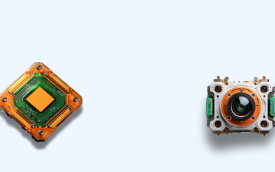
Better insights into component storage and manufacturing history can open up new avenues for a more resilient supply chain.


IPC standards ensure quality, reliability, and consistency in PCB design, manufacturing, and assembly. This guide covers key standards like IPC-A-610, IPC-2221, and IPC-J-STD-001, their importance, best practices, compliance challenges, and certification benefits.


Download the full infographic.


Nordic Semiconductor Introduces NTN Support and SIM Solution at Embedded World 2025

A countersink in PCB design is a conical recess that allows flat-head screws to sit flush with the board surface. This article explores countersinks vs. counterbores, when to use them, IPC standards, manufacturing considerations, and best practices to ensure reliable, cost-effective PCB designs.


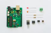
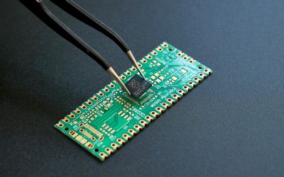
This article provides an in-depth overview of the various PCB components that make up electronic circuits – from passive elements like resistors and capacitors to active semiconductors and electromechanical devices.

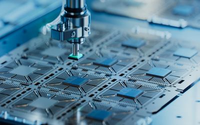
OSAT (Outsourced Semiconductor Assembly and Test) firms package, assemble, and test chips for fabless companies and foundries. As chip complexity rises, they boost efficiency, lower costs, and speed market entry for AI, IoT, and HPC. This article reviews OSAT fundamentals, players, and trends.


Researchers developed a scalable, low-cost device that can generate high-power terahertz waves on a chip, without bulky silicon lenses.

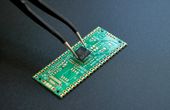
The guide to understanding the current state of the art in hardware & software for Edge AI.

Many of the long-held beliefs surrounding date codes have been empirically proven erroneous.

While rooted in historical necessity, date codes are being rendered antiquated by modern practices and standards.


The Importance of Traceability in Semiconductor Reliability and Supply Chain Resilience

Cornell scientists have developed a novel technique to transform symmetrical semiconductor particles into intricately twisted, spiral structures – or “chiral” materials – producing films with extraordinary light-bending properties.

3 minutes read