LGA vs BGA How to Select the Best IC Package for Your Design
LGA uses flat pads for connections, while BGA relies on solder balls for permanent mounting. This guide compares their thermal performance, electrical traits, reliability, and assembly pros and cons to help you choose the best IC package for your needs.

07 May, 2025. 9 minutes read
Introduction
Choosing between Land Grid Array (LGA) and Ball Grid Array (BGA) packaging is a big deal when designing high-performance electronics. This decision affects everything—from how well your device handles heat and maintains signal quality, to how easy it is to manufacture and how long it’ll last in the real world.
Both LGA and BGA were created to solve the same basic challenge: how to connect today’s complex integrated circuits, with hundreds or even thousands of input/output (I/O) pins, to a printed circuit board (PCB). But they go about it in very different ways. LGA uses flat contact pads, while BGA relies on tiny solder balls. That simple difference leads to major trade-offs depending on your application.
LGA is often the go-to for systems where you need strong thermal performance and the option to swap out components later—think high-end server processors or mission-critical aerospace tech. On the other hand, BGA's dense grid of solder balls allows for incredible electrical performance and saves space, making it ideal for smartphones, tablets, and high-speed computing devices.
And as chip designs grow more complex—some now with more than 5,000 pins—getting the packaging right is more critical than ever. A mistake here isn’t just inconvenient; it can delay entire product launches.
Overview of LGA and BGA Technologies
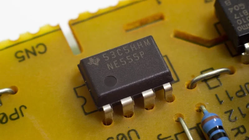
Land Grid Array (LGA) and Ball Grid Array (BGA) are two common high-density IC packaging types that connect chips to PCBs. Both employ a grid of I/O connections on the package underside, but differ fundamentally in how these connections are formed.
LGA packages use flat conductive pads—known as lands—that align with corresponding PCB pads. These chips can be socketed, enabling easy removal (e.g., in server CPUs), or soldered directly using paste. With no protruding elements, LGAs offer a low-profile form factor and excellent thermal transfer. Stand-off height is minimal, typically around 0.06–0.10 mm, making them ideal where space or cooling is critical.
In contrast, BGA packages feature pre-attached solder balls that are reflowed onto PCB pads during assembly, forming both electrical and mechanical bonds. This design supports extremely high pin density and compact layouts—ideal for mobile devices, GPUs, and FPGAs with 1,000+ I/Os. BGA balls also elevate the package (~0.5 mm), aiding in heat dissipation and inspection.
While LGA offers socketing flexibility and efficient heat transfer, BGA excels in miniaturization and signal integrity. The choice depends on application needs—serviceability and thermal demands favor LGA, while space-saving and high-speed interconnects favor BGA.
Recommended reading: IC Package Types: A Comprehensive Guide
Assembly and Manufacturing Considerations
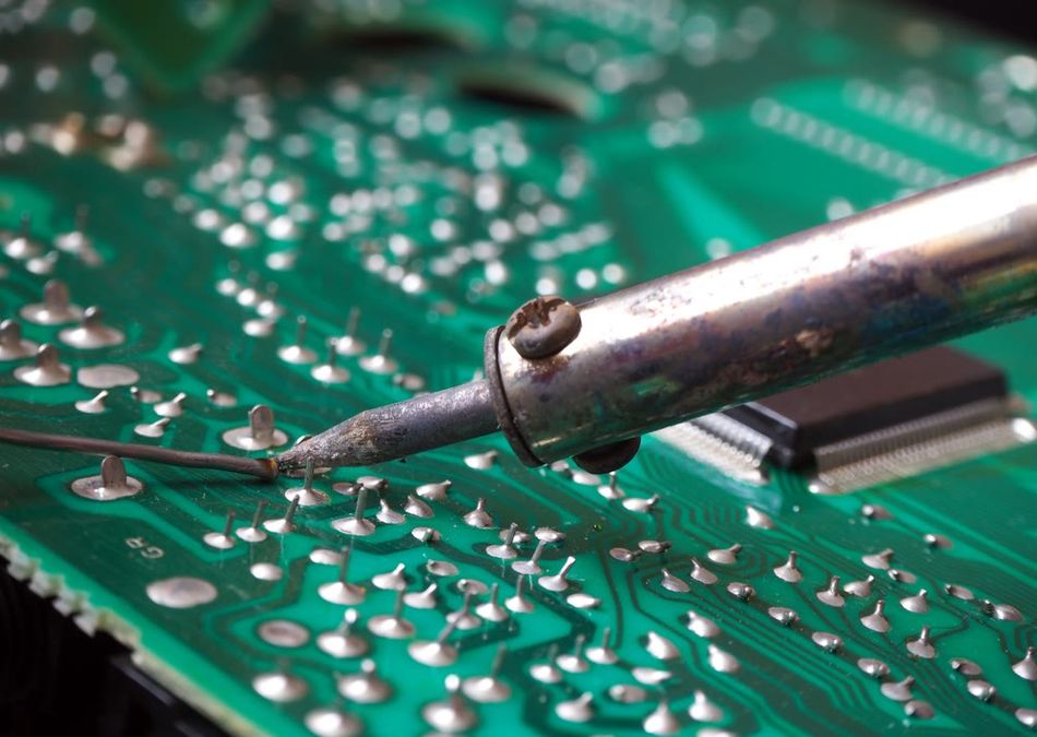
Implementing Land Grid Array (LGA) and Ball Grid Array (BGA) devices on a PCB demands precision in footprint design, soldering, and inspection. Both package types use copper pad arrays aligned to their respective terminal layouts—BGAs with solder balls, LGAs with flat contact pads. IPC-7095 (for BGA) and IPC-7093 (for LGA) recommend using non-solder-mask-defined (NSMD) pads, which promote better solder joint reliability by allowing solder to wet pad edges. During reflow, BGA solder balls melt and self-align with PCB pads, while LGAs rely entirely on solder paste applied to the board. Despite lacking solder balls, LGAs also self-center during reflow due to surface tension.
Reflow profiles for both packages are comparable, and both must meet JEDEC standards (e.g., J-STD-020). LGAs, however, have a much lower standoff (~0.06–0.1 mm), making cleaning beneath them harder than BGAs. For inspection, both require X-rays since joints are hidden. In socketed applications (common with LGAs in CPUs), additional assembly steps and board space must be considered. Routing complexity is similar, especially for high-density layouts, though LGAs allow slightly more flexibility in pad design. Ultimately, BGAs cost more due to ball attachment, while LGAs demand more precise solder paste control. Both are SMT-compatible and widely used in modern electronics.
Recommended reading: IPC Standards: The Definitive Guide for Electronics Engineers and PCB Designers
Thermal and Electrical Performance Comparison
In high-performance electronics, both thermal dissipation and signal integrity are critical. Ball Grid Array (BGA) and Land Grid Array (LGA) packages offer advantages over traditional leaded packages due to their compact form factors and optimized electrical paths.
Thermal Performance
BGA packages are widely recognized for their efficient thermal conduction. The solder balls underneath the chip enable direct heat transfer into the PCB’s copper layers. Some designs utilize a central cluster of thermal balls aligned with thermal vias to spread heat into the board’s internal layers. Additionally, BGAs often support top-side cooling with heat spreaders or heatsinks, offering dual thermal paths—through the PCB and externally. However, due to the limited surface area of each solder ball, effective thermal performance relies heavily on PCB design, including copper planes and thermal vias.
LGA packages approach thermal management differently. Socketed LGAs, such as those used in desktop CPUs, depend almost entirely on top-side cooling via heat spreaders and heatsinks. However, soldered LGAs (common in power modules and RF applications) can provide excellent thermal conduction through large exposed pads directly soldered to the PCB. This solid metal-to-metal interface often outperforms BGAs in thermal resistance. For enhanced performance, designers may incorporate thermal interface materials (TIMs) or dummy thermal pads connected to internal vias.
Electrical Performance
Both BGA and LGA offer excellent electrical characteristics. BGAs benefit from short interconnect paths, reducing inductance and maintaining high signal integrity. LGAs, especially when soldered, provide even shorter electrical paths, making them suitable for high-frequency applications such as RF and microwave systems.
While soldered LGAs and BGAs perform similarly, socketed LGAs introduce parasitic inductance due to spring contacts and potential air gaps. This makes them less ideal for ultra-high-speed or sensitive analog signals, although they are still suitable for GHz-range digital applications with proper design.
In terms of power delivery, both packages can support robust PDNs, especially when multiple power/ground connections are used. However, soldered packages—whether LGA or BGA—generally offer lower resistance and inductance compared to socketed options.
LGA vs. BGA: Long-Term Reliability, Reworkability, and Inspection
Beyond initial performance, engineers must consider solder joint reliability, ease of rework, and inspection options when choosing between LGA (Land Grid Array) and BGA (Ball Grid Array) packages.
Mechanical Reliability
Historically, BGAs were criticized for solder joint fatigue due to their stiff, ball-shaped interconnects that absorb strain from temperature changes or board flexing. LGAs, with even thinner joints, were once thought to be more vulnerable. However, modern lead-free solder like SAC305 flips this assumption. LGA solder joints, thanks to their smaller volume, solidify with a fine-grain structure that resists fatigue better than the coarse "beach ball" grain of BGAs. Studies by Flex Power Modules and Amkor show LGA joints may outperform BGA joints under thermal cycling. In shock or vibration scenarios, soldered BGAs with underfill excel in durability, especially in mobile or automotive uses. Socketed LGAs, however, risk contact fretting unless properly secured.
Reworkability
Reworking BGAs is complex. Specialized rework stations are needed, and reballing a removed chip is time-consuming and often impractical, especially if underfill was used. In contrast, soldered LGAs are easier to rework—no balls to replace, and often reusable after pad cleaning. Socketed LGAs are the most rework-friendly: no soldering required, just pop the chip in or out. This makes LGAs ideal for prototypes or mission-critical systems needing field repairs.
Inspection & Testing
Both BGA and LGA suffer from hidden solder joints, limiting visual inspection. Automated Optical Inspection (AOI) can check placement but not joint integrity. X-ray imaging is the go-to for both, revealing voids, shorts, or missing joints. Routine X-ray adds cost, so some rely on electrical testing like boundary scan (JTAG) or In-Circuit Testing (ICT) for fault detection. One slight advantage of LGA is that socketed versions eliminate the need for solder joint inspection.
Recommended reading: PCB Inspection: Ensuring Quality and Reliability in Electronics Manufacturing
LGA vs BGA: Technical Comparison Matrix
Parameter | LGA (Land Grid Array) | BGA (Ball Grid Array) |
Connection Method | Flat copper lands (Au/Ni finish) | SAC305 solder spheres (Ø0.25-0.76mm) |
Assembly Process | • Socketed (ZIF/LIF) • Soldered (paste deposition) | • Reflow soldering only • Self-aligns (±150µm) |
Package Density | • 0.5-1.0mm pitch typical • Max ~2000 pads (LGA4677) | • 0.3-1.0mm pitch • >5000 balls (HPC FPGAs) |
Standoff Height | • Soldered: 50-100µm • Socketed: 2-5mm | 300-500µm (post-reflow) |
Thermal Performance | • θJA: 15-25°C/W (soldered) • 30-50°C/W (socketed) • Direct metal-PCB interface | • θJA: 20-35°C/W • Thermal balls (20-30% array) • Requires thermal vias |
Electrical Characteristics | • 0.1-0.3nH inductance (soldered) • 0.5-2nH (socketed) • Suitable for ≤10Gbps (socketed) | • 0.2-0.5nH inductance • Supports 112Gbps SerDes • Symmetric return paths |
Reliability Data | • 3500-5000 thermal cycles (-40°C to +125°C) • No solder fatigue in sockets | • 2500-4000 thermal cycles • Requires underfill for shock resistance |
Rework Complexity | • Hot air removal (300°C) • No reballing needed • Socket swap <5min | • IR preheat + hot gas • Reballing required • 3-5x higher cost |
Inspection Method | • X-ray (2D/3D) • Socket contacts are visible when disassembled | • Mandatory X-ray • Acoustic microscopy for voids |
Cost Factors | • No ball attachment cost • Socket adds 5− 5−50/BOM • Lower volume pricing | • Ball attach adds 8-12% • Higher layer count PCBs • Better at scale |
Optimal Use Cases | • Server CPUs • Field-replaceable modules • High-power RF (>30W) | • Mobile SoCs • HPC GPUs/FPGAs • Memory packages |
Conclusion
Land Grid Array (LGA) and Ball Grid Array (BGA) are widely used in modern electronics, each offering distinct benefits. BGA packages support high pin counts and compact designs, making them ideal for high-performance, high-density applications. LGA, by contrast, provides easier rework and socketing options, useful for prototyping and scenarios needing component upgrades or replacements. Choosing between the two depends on design priorities: miniaturization and volume production favor BGA, while serviceability and prototyping ease favor LGA.
Engineers should also consider component availability, assembly capabilities, and testing requirements. For BGA, ensure proper reflow processes and X-ray inspection; for LGA, focus on accurate solder paste application. Always follow IPC layout guidelines and plan for future scalability if upgrades might be needed. In many systems, both types are used strategically—for example, soldered BGAs for most components and an LGA socket for the main processor. Understanding these trade-offs helps ensure reliable, efficient, and scalable product design.
FAQs
Q1: What is the main difference between LGA and BGA packaging?
A1: The key difference lies in how the chip connects to the PCB.
LGA (Land Grid Array) uses flat metal pads (“lands”) on the underside of the chip. These pads are either soldered with paste or connected via a socket.
BGA (Ball Grid Array) has tiny solder balls pre-attached in a grid pattern. These balls melt and bond to the PCB during reflow soldering.
In short:
LGA = Lands (no solder balls)
BGA = Balls (pre-applied solder)
This results in different assembly methods: LGA can be socketed or soldered; BGA is always soldered.
Q2: Why do desktop CPUs use LGA sockets while laptop CPUs use BGA?
A2: Desktop CPUs use LGA sockets for easy upgrades and servicing — users can swap or replace CPUs. LGA sockets also handle higher pin counts and support robust heatsinks.
Laptop CPUs use BGA because they’re soldered directly onto the motherboard. This saves space, reduces profile height, and slightly lowers cost — ideal for slim, portable designs.
Summary:
Desktops = LGA for flexibility and serviceability
Laptops = BGA for compact, permanent integration
Q3: Which is better for high reliability under temperature cycling: LGA or BGA?
A3: Both can be reliable, but it depends on the design.
Recent studies show lead-free LGA joints can outperform BGA in thermal cycling due to their smaller solder volumes and stronger grain structures. However, BGA can also be highly reliable, especially when paired with matching PCB materials and optional underfill for stress reduction.
If extreme reliability is a concern:
LGA may offer longer fatigue life due to lower standoff.
BGA needs proper thermal matching and possibly underfill.
Bottom line: Neither is inherently inferior — reliability depends on the design and materials used.
Q4: Can I hand-solder or prototype with BGA and LGA components?
A4:
BGA: Not suitable for hand-soldering. Reflow soldering and X-ray inspection are usually required. Some low-temp or hot-air tricks exist but are challenging and unreliable.
LGA: Easier to rework by hand, especially if it has an exposed pad. Similar to QFN packages, you can apply solder paste and use a heat gun from below.
Prototyping tips:
Use evaluation boards or breakouts (pre-mounted chips on small PCBs).
Use sockets if available.
For both types, reflow tools are generally required.
Summary: LGA is more prototype-friendly; BGA needs specialized equipment and inspection.
Q5: How do I inspect solder joints on LGAs or BGAs?
A5: Since joints are hidden underneath, you can’t inspect them visually. Instead, use:
X-ray imaging: Reveals solder joint shapes, voids, bridges, and alignment.
Electrical testing: JTAG/boundary scan can check connectivity.
In-circuit testing (ICT): Detects opens/shorts on accessible nets.
For LGA in sockets, running the system is often the test — any poor contact causes functional failure.
Summary:
X-ray is the most reliable method.
Use proper reflow process control and testing if you don’t have inspection tools.
Q6: Are LGAs always socketed? Can they be soldered directly?
A6:
No — LGAs don’t have to be socketed. While desktop CPUs often use LGA sockets, many smaller chips (like modules and ICs) come in LGA form and are intended for direct soldering to the PCB with paste — no socket involved.
Key point:
LGA = land pads (no solder balls)
Whether it’s soldered or socketed depends on the application and form factor.
BGA, in contrast, is always soldered — sockets for BGA are rare and expensive (mainly for testing).
Q7: What standards or guidelines should I follow when designing with BGA or LGA?
A7: Consider these key references:
IPC-7095: Design and assembly guide for BGAs (pad design, voids, inspection tips).
IPC-7093: Guide for bottom-terminated components (LGA, QFN). Covers land patterns, stencil design, and the soldering process.
JEDEC MO Series: Standardizes package outlines (e.g., BGA ball pitch, LGA dimensions).
IPC-A-610: Acceptance criteria for solder joints (includes BGA void standards).
JESD22-A113/B102: Guidelines for reliability testing of solder joints under stress.
Manufacturer application notes: Always check the vendor’s recommendations for reflow profiles, land pattern designs, and soldering methods.
References
LionCircuits, "LGA vs. BGA: A Comprehensive Guide," LionCircuits Blog, [Online]. Available: https://www.lioncircuits.com/blog/posts/lga-vs-bga/
InOrigin, "Considerations for Designing for Assembly," [Online]. Available: https://www.inorigin.eu/considerations-for-designing-for-assembly/
GlobalWellPCBA, "BGA vs LGA: Key Differences, Benefits & Applications," GlobalWellPCBA Blog, [Online]. Available: https://www.globalwellpcba.com/bga-vs-lga/
U. Waseem, "PCB Inspection: Ensuring Quality and Reliability in Electronics Manufacturing," Wevolver, May 21, 2024. [Online]. Available: https://www.wevolver.com/article/pcb-inspection
PCBTok, "Comparing the Difference of LGA vs BGA," PCBTok Blog, [Online]. Available: https://www.pcbtok.com/lga-vs-bga/
in this article
1. Introduction2. Overview of LGA and BGA Technologies3. Assembly and Manufacturing Considerations4. Thermal and Electrical Performance ComparisonLGA vs. BGA: Long-Term Reliability, Reworkability, and Inspection6. LGA vs BGA: Technical Comparison Matrix7. Conclusion8. FAQs9. References