Featured
High-frequency circuits-like those utilized in microcells and DAS-are more sensitive to PCB material selection, fabrication, and assembly.

High-frequency circuits-like those utilized in microcells and DAS-are more sensitive to PCB material selection, fabrication, and assembly.
High-frequency circuits-like those utilized in microcells and DAS-are more sensitive to PCB material selection, fabrication, and assembly.
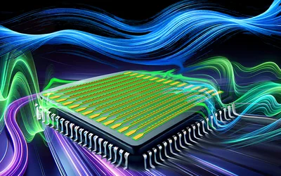
Lightwave electronics aim to integrate optical and electronic systems at incredibly high speeds, leveraging the ultrafast oscillations of light fields.
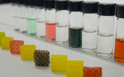
It’s a step toward smart coatings that change color—or other properties—on the fly.
Controlled impedance is the control of PCB trace impedance within specified tolerances. This article covers microstrip and stripline designs, IPC-2141A formulas, stackup selection, impedance tolerances, routing practices, and TDR testing for signal integrity.
16 minutes read.
16 minutes read.
12 minutes read.

Additive Manufacturing
The ever growing need for precise micro-parts is restricted by current tech...
1 Post

Machinery Manufacturing
We Are Giving Human Materials the Superpowers of Nature Using Lasers
1 Post

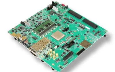
Explore AMD's Zynq UltraScale+ MPSoC and RFSoC for 5G, ADAS, and embedded applications.
Discover how wireless technologies like 5G, LoRa, Wi-Fi, and Zigbee are transforming industrial automation by enabling flexible, scalable, and cost-efficient connectivity.
Discover how 5G RedCap enables cost-efficient, low-power connectivity for industrial gateways and rugged IoT, bridging the gap between LTE and full 5G performance.
Controlled impedance is the control of PCB trace impedance within specified tolerances. This article covers microstrip and stripline designs, IPC-2141A formulas, stackup selection, impedance tolerances, routing practices, and TDR testing for signal integrity.
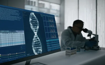
New System Strengthens Security for the Biotech Industry
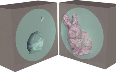
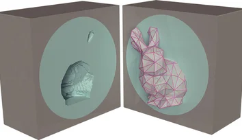
Whether designing a window in an airliner or a cable conduit for an engine, manufacturers devote a lot of effort to reinforcing openings for structural integrity. But the reinforcement is rarely perfect and often creates structural weaknesses elsewhere.
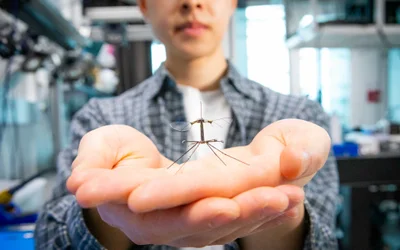
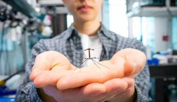
Microrobot gets crane fly-inspired legs for soft touchdowns
High-frequency circuits-like those utilized in microcells and DAS-are more sensitive to PCB material selection, fabrication, and assembly.

8 minutes read
Lightwave electronics aim to integrate optical and electronic systems at incredibly high speeds, leveraging the ultrafast oscillations of light fields.
It’s a step toward smart coatings that change color—or other properties—on the fly.

4 minutes read
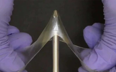
Soft polymers with the combined properties of electrolytes and traditional polymers offer some unique and desirable properties that can be drastically changed on demand.

5 minutes read
Stanford scientists designed a catalyst that turns carbon dioxide into ethanol, which could incentivize cleaning up emissions.

4 minutes read
EPFL scientists have developed an AI-based technique to improve chemical analysis of nanomaterials, overcoming challenges of noisy data and mixed signals.

3 minutes read
The lightweight material could extend EV range or fuel efficiency once its microstructure is understood.
3 minutes read
Penn State scientists recently found that mass-produced soda-lime silicate glass from post-consumer bottles of different colors can be safely melted together in the recycling process, which could potentially lead to more bottles being recycled.

3 minutes read
Explore the future of connected communities in intelligent cities and underserved regions, highlighting the role of technologies like 5G, AI, and blockchain in enhancing connectivity and promoting inclusive development.
Researchers have created a new class of materials called “glassy gels” that are very hard and difficult to break despite containing more than 50% liquid. Coupled with the fact that glassy gels are simple to produce, the material holds promise for a variety of applications.

3 minutes read
Combining a deep curiosity and “recreational biology,” Stanford researchers have discovered how a simple cell produces remarkably complex behavior, all without a nervous system. It’s origami, they say.
4 minutes read
The work could lead to ultra-efficient electronics and more.
The future of data, Edge Data Center, is equivalent to a mini data centre. Its proximity to enterprises eliminates latency and other limitations, giving access to real-time data. In this article, we will delve into its core concepts, advancements, operational challenges, and real-time applications.
Smaller than a coin, this optical device could enable rapid prototyping on the go.
In this episode, discuss how big of a problem lead contaminated water still is across the world and how a collaboration between MIT & Nanyang University plans to tackle it with a highly accurate and inexpensive water pollution sensor.

16 minutes read