Zynq UltraScale+: AMD's Heterogeneous MPSoC and RFSoC
Explore AMD's Zynq UltraScale+ MPSoC and RFSoC for 5G, ADAS, and embedded applications.

02 Jul, 2026. 16 minutes read
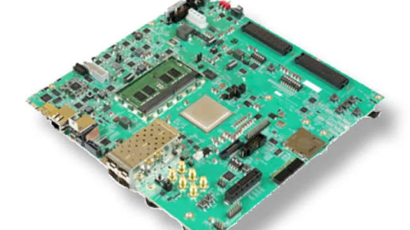
Defense-Grade AMD Zynq UltraScale+ XQ MPSoCs
Key Takeaways
Heterogeneous architecture: Zynq UltraScale+ combines a processing system (PS) built around dual- or quad-core Arm Cortex-A53 application processors, dual-core Arm Cortex-R5F real-time cores and, on EG/EV parts, a Mali-400 MP2 GPU. The PS sits beside a programmable logic (PL) fabric with hundreds of thousands of system-logic cells, DSP slices, block RAM, and UltraRAM, all fabricated on TSMC's 16 nm FinFET process [1].
Rich memory and I/O: The PS integrates a multi-protocol DDR4, DDR3, DDR3L, LPDDR3, and LPDDR4 memory controller that supports 32-bit or 64-bit interfaces with ECC[1]. On-chip memory includes 256 kB of PS RAM and tens of megabits of block RAM and UltraRAM in the PL[1]. High-bandwidth AXI ports connect the PS and PL, including high-performance (HP), high-performance coherent (HPC), and accelerator-coherency (ACP) interfaces for cache-coherent or non-coherent transfers.
Multiple sub-families: CG devices offer dual-core A53 processors; EG devices add quad-core A53 and a Mali-400 MP2 GPU; EV devices further integrate a hardened H.264/H.265 video-codec unit[2]. Zynq UltraScale+ RFSoC variants embed multi-giga-sample RF ADCs and DACs and optional LDPC/turbo FEC cores for single-chip radios[3].
Power domains and security: The PS is partitioned into full-power (FPD), low-power (LPD) and battery-powered (BPD) domains; the PL can be powered independently[1]. Secure boot uses AES-GCM and SHA-3/384 with 4096-bit RSA authentication[1], and the product selection guide lists RSA, AES, and SHA hardware in the security block[2].
Development ecosystem: Hardware is designed with Vivado and high-level synthesis; software runs on Vitis (unified software platform) and PetaLinux for embedded Linux[4]. Vitis AI supplies optimized AI accelerators, enabling edge inference on Zynq.
Introduction
Zynq UltraScale+ is AMD's (formerly Xilinx) adaptive system-on-chip officially known as Zynq® UltraScale+™ MPSoC, that fuses a complete 64-bit multicore processing system with UltraScale programmable logic. First shipped in 2015 on a 16 nm FinFET process, the family extends the company's original Zynq-7000 series (28 nm, Cortex-A9) with higher performance, richer peripherals and a focus on deterministic compute. The architecture integrates quad-core Arm Cortex-A53 or dual-core variations for running Linux or high-level operating systems, dual-core Arm Cortex-R5F for real-time tasks, optional graphics and video engines, a platform management and security subsystem, and a large FPGA fabric. This unique combination lets system architects partition workloads into software running on familiar Arm cores and custom hardware accelerators in programmable logic, achieving high throughput and low latency in a power-efficient form factor. The Zynq UltraScale+ portfolio further includes RFSoC devices that integrate multi-gigahertz RF analog converters and forward-error-correction logic for single-chip radio applications.
The article assumes that you understand FPGA fundamentals; for basics, see the "What Is FPGA?". The sections below focus on what makes Zynq UltraScale+ distinctive: its processing-system-plus-programmable-logic architecture, the CG/EG/EV and RFSoC sub-families, memory and interconnect, power and security features, tool flow and development ecosystem, target applications, and guidance on choosing the right device.
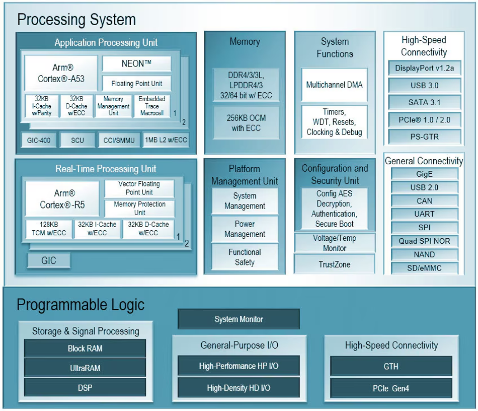
Block diagram of the AMD Zynq UltraScale+ MPSoC architecture, showing the integrated processing system, programmable logic fabric, memory subsystems, security functions, and high-speed connectivity interfaces. Source: AMD
What is Zynq UltraScale+?
Zynq UltraScale+ is AMD's family of adaptive system-on-chip (SoC) devices that combines a complete 64-bit multicore processor subsystem with UltraScale+ FPGA programmable logic on a single 16 nm chip. Unlike a standalone FPGA, which requires an external processor, or a standalone SoC, which lacks reconfigurable hardware, Zynq UltraScale+ integrates both — letting designers run software on Arm cores while offloading time-critical or compute-intensive tasks to custom hardware in the programmable logic fabric. The family includes MPSoC devices for embedded compute, vision, and industrial applications, and RFSoC devices that add integrated RF data converters for wireless and radar systems. If you are new to FPGAs, see our [What Is FPGA?] guide before continuing.
Recommended Reading: FPGA Chip: Architecture, Fabrication, and Families
Zynq UltraScale+ Architecture: Processing System and Programmable Logic
Processing System (PS)
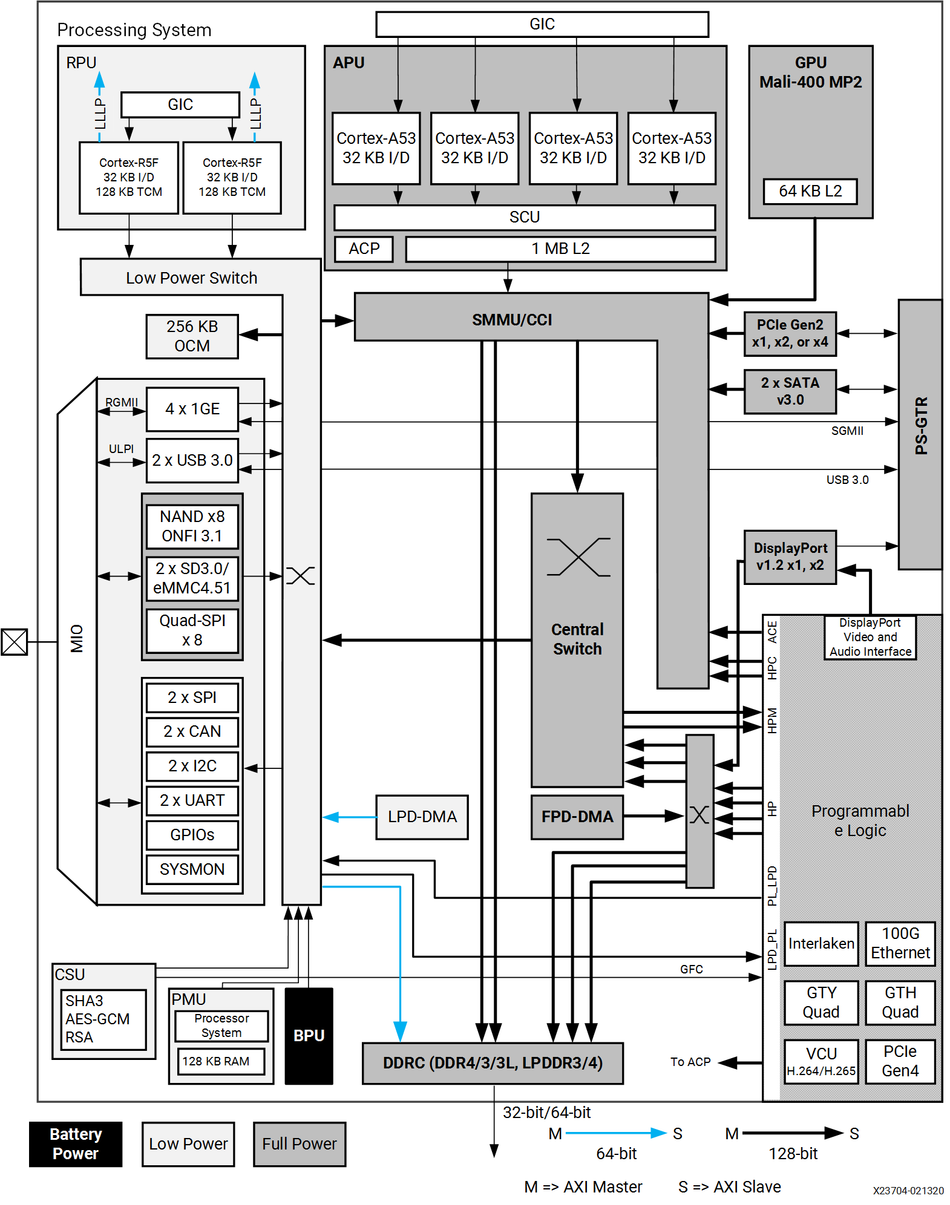
The PS implements a heterogeneous cluster of hardened processors and peripherals on a shared interconnect. According to the Zynq UltraScale+ data sheet[1], the PS integrates:
Application processing unit (APU): Up to four 64-bit Arm Cortex-A53 cores (dual-core on CG devices, quad-core on EG/EV/RFSoC), running up to 1.5 GHz [1]. The APU supports Armv8-A with 64-bit and 32-bit modes, TrustZone, NEON SIMD, floating-point, and CoreSight debug and trace[1]. Each core has 32 kB instruction and 32 kB data caches with ECC[1], and the cluster shares a 1 MB L2 cache[1]. The APU includes an Accelerator-Coherency Port (ACP) and AXI Coherency Extension (ACE) to allow PL masters to read/write cached data [1].
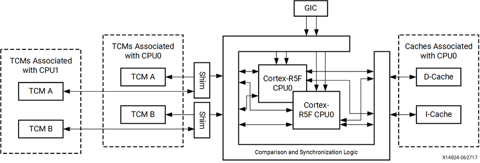
Real-time processing unit (RPU): A dual-core Arm Cortex-R5 MPCore (Cortex-R5F) subsystem, clocked up to 600 MHz [1]. It supports Armv7-R with lock-step or independent operation, separate 32 kB instruction and data caches with ECC, and 128 kB tightly coupled memories (TCMs) per core [1]. The RPU is ideal for deterministic control loops, safety-critical code or bare-metal tasks.
Graphics processing unit (GPU): EG and EV devices include an Arm Mali-400 MP2 GPU. The GPU supports OpenGL ES 1.1/2.0 and OpenVG 1.1, runs up to 667 MHz, and comprises a single geometry processor and two pixel processors with a 64 kB L2 cache [1]. It accelerates 2D/3D graphics and overlays for HMIs or vision applications.
Video codec unit (VCU): EV devices integrate a hardened H.264/H.265 encoder/decoder that supports full-HD video and reduces PL resource usage [2].
Platform management and security: The Platform Management Unit (PMU) monitors supply rails, initiates resets and manages system power; the Configuration Security Unit (CSU) performs secure boot, key management and device configuration. Secure boot uses AES-GCM and SHA-3/384 with 4096-bit RSA authentication [1]. The product selection guide lists RSA, AES and SHA hardware blocks and an AMS voltage/temperature monitor as part of the power management and security infrastructure [2].
Memory subsystem: An integrated multi-protocol dynamic memory controller supports 32-bit or 64-bit DDR4, DDR3, DDR3L or LPDDR3 interfaces and a 32-bit LPDDR4 interface with ECC [1]. Up to 32 GB of external memory can be addressed [1]. On-chip PS memory provides 256 kB of RAM with ECC [1], while the PL offers up to 36 Mb UltraRAM, 35 Mb block RAM and 11 Mb distributed RAM [1].
Peripheral connectivity: The PS includes PCIe Gen2 x4, SATA 3.1, USB 3.0, DisplayPort, quad Gbit Ethernet MACs, SD/eMMC, quad-SPI, CAN, I2C, SPI and UART interfaces, and general purpose I/O via PS MIO pins [2]. Additional GPIO (general-purpose I/O) resources provide flexible board-level interfacing for sensors, control signals, and embedded peripherals.
These hardened processors and peripherals provide a deterministic and power-efficient platform for software tasks that do not require hardware acceleration. By integrating them with the PL, designers gain a tight coupling between software and custom logic.
Recommended Reading: FPGA Chip: Architecture, Fabrication, and Families
Programmable Logic (PL)
The PL is based on the UltraScale architecture. It offers:
System logic cells: 81K to over 1.1 M system logic cells (SLCs) depending on device size [2]. Each SLC includes look-up tables (LUTs) and flip-flops, grouped into configurable logic blocks (CLBs).
Memory: Each device includes distributed RAM, block RAM, and UltraRAM, totaling up to tens of megabits[1][2]. Block RAM tiles provide 36 kbit dual-port memory; UltraRAM tiles provide 288 kbit memory with high bandwidth and low dynamic power.
DSP slices: UltraScale DSP48E2 slices perform 27 × 18-bit multiplications with accumulators and logic, enabling high-performance FIR filters, FFTs and AI inference. Device counts range from 216 to more than 3528 slices [2]. RFSoC devices allocate over 4272 DSP slices for baseband processing [3].
High-speed serial transceivers: The PL integrates GTH transceivers capable of line rates up to ~16.3 Gb/s and, in some EG devices, GTY transceivers up to ~32.75 Gb/s [2]. Additionally, PS-side GTR transceivers (up to 6 Gb/s) support SATA, PCIe Gen2, and DisplayPort [1].
PS-PL AXI interfaces: Twelve 32/64/128-bit AXI4 ports connect the PS and PL [2]. High-performance ports provide non-coherent high-bandwidth access to DDR; high-performance coherent (HPC) ports attach to the CCI-400 interconnect and maintain cache coherency; the Accelerator-Coherency Port (ACP) allows PL masters to read/write the APU cache with minimal maintenance. These interfaces enable tight coupling between software and hardware accelerators.
Zynq UltraScale+ MPSoC Device Hardware Architecture. Source: AMD
Zynq UltraScale+ Sub-families: CG, EG, EV, and RFSoC Compared
The family is divided into CG, EG, EV, and RFSoC variants. CG devices provide a minimal baseline; EG adds more cores and a GPU; EV adds a video codec; RFSoC devices integrate analog converters. Table 1 compares the key features.
Variant | APU | RPU | GPU | Video Codec | PL logic cells (range) | GTH/GTY transceivers | Typical use cases |
CG | Dual-core A53 up to 1.3 GHz[2] | Dual-core R5F up to 533 MHz[2] | None | None | 81 k-600 k SLCs[2] | Up to 24 GTH transceivers (16.3 Gb/s)[2] | Cost-optimized control and gateway applications |
EG | Quad-core A53 up to 1.5 GHz[2] | Dual-core R5F up to 600 MHz[2] | Mali-400 MP2 GPU[1] | None | 81 k-1.143 M SLCs[2] | GTH and, on larger parts, GTY transceivers (32.75 Gb/s)[2] | HMIs, vision, embedded compute, 5G baseband |
EV | Quad-core A53 up to 1.5 GHz[2] | Dual-core R5F up to 600 MHz[2] | Mali-400 MP2[2] | Hardened H.264/H.265 VCU[2] | 192-504 k SLCs[2] | Up to 24 GTH (16.3 Gb/s) | Embedded video processing, surveillance, automotive ADAS |
RFSoC (Gen 1-3 & DFE) | Quad-core A53 up to 1.5 GHz[3] | Dual-core R5F up to 600 MHz | None | None | 678 k-930 k SLCs [3] | Up to 16 GTY transceivers (28.21 Gb/s) | Single-chip radio with integrated RF converters, 5G massive MIMO, cable Remote-PHY, radar |
Further Reading: A Comprehensive Guide to FPGA Development Boards
Comparison to Other AMD Adaptive SoCs
Zynq UltraScale+ sits between the earlier Zynq-7000 series and the newer Versal adaptive SoC. Relative to the 28 nm Zynq-7000 (dual-core Cortex-A9), UltraScale+ offers 64-bit A53 processing, a high-performance R5F real-time complex, significantly higher logic density, UltraRAM, GTH/GTY transceivers, and a secure boot architecture. Versal, fabricated on a 7 nm-class process, replaces the crossbar with a network-on-chip, adds AI Engine vector processors and DSP blocks, and trades the on-chip GPU for AI Engine array acceleration instead. Designers choose UltraScale+ when they need higher determinism, established tool flows, and integrated analog (RFSoC) without the complexity and cost of Versal.
Memory, Interconnect, and Coherency
External and On-chip Memory
Zynq UltraScale+ MPSoC multi-protocol memory controller supports 32-bit or 64-bit DDR4/DDR3/LPDDR4/LPDDR3 with ECC and up to 32 GB capacity [1]. The wide memory channels provide the bulk storage for operating systems, data buffers, and video frames. The PL can access this memory via high-performance AXI ports.
On-chip memory is crucial for low-latency operations. The PS includes 256 kB of on-chip RAM (OCM) with ECC[1], used for boot code, real-time data or communication buffers. The PL integrates distributed RAM (small LUT-based memory), block RAM (36 kbit dual-port memory) and UltraRAM (288 kbit blocks), giving designers tens of megabits of on-chip storage [1]. The selection guide enumerates distributed RAM, block RAM and UltraRAM capacities across devices [2], enabling on-chip caches or scratchpads without external memory access.
AXI Interconnect and Coherency Mechanisms
The PS and PL communicate through a rich set of AXI interfaces, each optimized for different workloads:
High-performance (HP) ports bypass the cache-coherent interconnect and connect directly to the DDR controller. These 64- or 128-bit ports provide high-throughput DMA for bulk transfers but require software to bypass CPU caches to prevent stale data.
High-performance coherent (HPC) ports attach to the CCI-400 interconnect used by the APU, supporting ACE transactions. When configured correctly, HPC ports maintain coherence between PL masters and the APU caches, enabling shared data structures without explicit cache maintenance. HPC ports are generally preferred over the ACP for most designs because they offer higher bandwidth and do not disturb L2 cache contents[5].
Accelerator-coherency port (ACP) is a 64-bit interface to the APU's L2 cache. It is optimized for medium-grained accelerators that manipulate data in the CPU cache, such as cryptographic blocks or block-level video processing[5]. The ACP reduces software cache maintenance overhead by allowing PL masters to allocate and evict lines in the APU cache.
AXI Coherency Extension (ACE) is a 64-bit AXI4 interface to the APU that provides full two-way cache coherency between the PL and the Cortex-A53 processors. Unlike the ACP, which only snoops the APU's L2 cache, the ACE interface snoops accesses on both the CCI and the PL side, allowing a cached PL master (such as a MicroBlaze processor) to remain fully coherent with the Cortex-A53 caches in hardware [1]
The PS also exposes four general-purpose AXI slave interfaces for control/status registers and configuration, as well as an AXI master to access PL peripherals. These ports, combined with PL-side AXI interconnect, give designers flexibility to build custom memory hierarchies.
Power Management and Security
Low-power and safety features are critical in embedded and automotive applications. Zynq® UltraScale+TM MPSoC partitions the PS into multiple power domains[1]:
Full-power domain (FPD): Contains the APU, GPU, DDR controller, high-speed I/O, FPD-DMA and high-performance peripherals[1]. The FPD can be completely powered down for ultra-low-power modes if the workload only uses real-time cores.
Low-power domain (LPD): Houses the RPU, LP-DMA, PMU, CSU, low-speed I/O and static memory interfaces[1]. The LPD remains active for standby or deterministic control while the APU is off.
Battery-power domain (BPD): Retains only the real-time clock (RTC) and battery-backed RAM[1]; the rest of the PS is powered off.
The PL can also be powered down independently [1]. Software can gate clocks to unused peripherals and manage dynamic voltage scaling. Power Design Manager (PDM) software provides power-estimation tools[1].
Security features encompass encryption, authentication, and isolation:
Secure boot: During the multi-stage boot process, the CSU uses AES-GCM to decrypt and authenticate the bitstream and software images; a 4096-bit RSA block authenticates the image signature[1]. Boot devices (NAND, Quad-SPI, SD, eMMC, JTAG) are selected via mode pins[1]. First-stage bootloader (FSBL) runs from on-chip ROM and loads user-defined code[1].
Cryptographic hardware: The power-management and security block integrates RSA, AES, and SHA accelerators[2]. Designers can store keys in eFUSE or battery-backed RAM. TrustZone partitioning isolates secure and non-secure worlds on the APU [1].
Functional safety: Many devices support safety certification (IEC 61508, ISO 26262) using lock-step mode on the RPU, dual-redundant clocking with independent PLL support, and ECC on all memories. The product selection guide notes the presence of functional-safety features and system monitors[2].
Vivado, Vitis and Vitis AI: The Zynq UltraScale+ Design Flow
Designing with Zynq UltraScale+ spans both hardware and software domains.
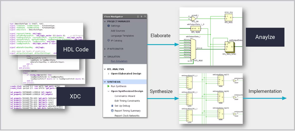
Hardware Design with Vivado
Vivado Design Suite is AMD's FPGA toolchain for UltraScale+ devices. It allows designers to create PL logic using schematics (Block Design), register-transfer level (RTL) code, or high-level synthesis. Vivado includes the IP Integrator for assembling IP blocks and generating a hardware design (XSA file). It also provides implementation, timing closure, bitstream generation, and hardware debugging. Vivado's power analysis works in concert with PDM to optimize power domains. For users migrating from the older ISE or Zynq-7000 flows, Vivado extends the concept of processing-system configuration to UltraScale+ features (memory mapping, I/O, security settings).
Software Design With Vitis and PetaLinux
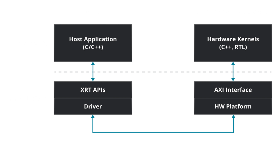
The Vitis unified software platform provides an integrated development environment (IDE) to build applications for the APU, RPU and PL accelerators. The Embedded Design Tutorial emphasises that installing the Vitis IDE automatically installs the Vivado Design Suite, unifying hardware and software flows[4]. Vitis includes compilers, debuggers, profilers, system simulation and libraries for C/C++ and OpenCL. It generates standalone bare-metal executables or uses PetaLinux for full Linux systems.
Vitis unified software platform. Source: AMD
PetaLinux Tools generate a customised embedded Linux distribution. The tutorial notes that PetaLinux must be installed on a Linux host; it produces board support packages (BSP), root file systems, device trees and kernel configurations for UltraScale+ boards[4]. Using PetaLinux with Vitis, designers can develop, deploy and debug Linux applications on the APU while using the RPU for real-time tasks.
Note: AMD has signaled a transition away from PetaLinux — EDF-based platforms are now the recommended flow for new Vitis designs, with PetaLinux-based platforms slated for removal in Vitis 2027.1. AMD's "Common Images" now provide a prebuilt Linux kernel, rootfs, and sysroot for legacy PetaLinux-based development without requiring PetaLinux Tools to be installed.
Vitis AI extends the toolchain to AI inference. It provides deep-learning processors (DPUs) as IP cores for the PL, model compression, quantisation tools and software libraries. Combined with the APU and PL, Vitis AI enables edge AI solutions such as image classification or object detection at low latency and power.
Hardware-software Co-design Workflow
Typical development flows:
Use Vivado IP Integrator to configure the processing system (APU/RPU, memory, I/O) and integrate PL IP cores (custom hardware accelerators or AMD IP such as DMA, AXI SmartConnect, Video PHY). Generate the hardware specification (XSA).
Use Vitis to create software platforms from the XSA, targeting bare-metal or Linux on the APU and optionally standalone code on the RPU. Develop C/C++ applications; build, run and debug via JTAG or remote debugging.
Use PetaLinux to configure and build a Linux distribution that includes necessary drivers for PL IP (e.g., video codec, DMA). Boot the system and run applications from SD/eMMC.
When AI workloads are involved, instantiate Vitis AI DPU IP in the PL, compile models and integrate them with software applications.
Zynq UltraScale+ RFSoC: Integrated Radio
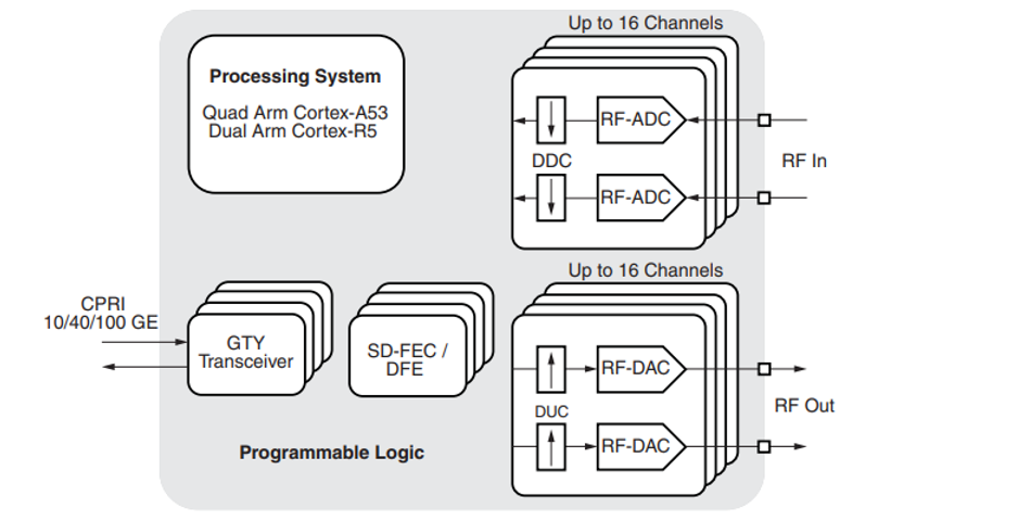
The RFSoC variants incorporate a high-performance RF data converter subsystem into the UltraScale+ MPSoC. Key features from AMD's RFSoC page include:
Integrated RF ADC/DAC: RFSoC devices embed up to sixteen 6.554 GSPS DACs and eight or sixteen 4.096 GSPS ADCs (Gen 1); later generations increase sample rates to 9.851 GSPS and input/output frequencies up to 7.125 GHz[3]. This eliminates external converters and JESD204B/C interfaces to those external chips.
Digital front-end and FEC: The architecture includes hardened digital front-end (DFE) units and optional soft-decision LDPC/turbo forward-error-correction cores alongside RS-FEC for high-speed transceivers that deliver over 1 Gb/s of throughput at low latency[3]. The DFE variant extends frequency coverage to 7.125 GHz and provides hardware support for 400 MHz bandwidth per antenna[3].
Complete SoC for radio: The RFSoC combines the same quad-core APU, dual-core RPU, PL fabric and security blocks used in UltraScale+ with the RF data converters, giving designers a single-chip software-defined radio platform[3]. Device portfolios (Gen 1/2/3 and DFE) offer different channel counts and sample rates[3].
Note: In November 2025, AMD introduced the Versal RF Series — built on the 7nm Versal architecture as its next-generation RF adaptive SoC, offering up to 80 TOPS of DSP compute and 32 GSPS/18 GHz RF converters. Versal RF targets the highest-end aerospace, defense, and test/measurement applications, while Zynq UltraScale+ RFSoC remains a proven, cost-effective choice for established 5G and cable infrastructure designs.
RFSoC's integrated analog significantly reduces board area, power and system cost compared with discrete RF ADC/DAC modules. Applications include 5G New Radio massive MIMO base stations, cable Remote-PHY nodes, phased-array radar and wideband test equipment[3]. The ability to update modulation, filtering and FEC in software and programmable logic makes RFSoC attractive for evolving standards.
Applications and Use Cases
Zynq UltraScale+ devices serve a broad range of embedded applications where deterministic performance, low latency, and system integration matter:
5G wireless infrastructure: UltraScale+ EG devices and RFSoC variants implement baseband processing, beamforming and digital front-end functions for macro and small-cell radios. The RFSoC's integrated converters and FEC simplify Massive MIMO and Remote-PHY equipment [3].
Automotive ADAS and autonomous drive: EG and EV devices provide high compute, a GPU for graphics, and a VCU for multi-stream video encoding/decoding. Real-time processing (RPU), hardware acceleration (PL), and functional safety features enable perception, sensor fusion, and camera monitoring. ISO 26262 support helps achieve automotive ASIL ratings.
Aerospace and defense: UltraScale+ devices are used in mission computers, radar, secure communications, and electronic warfare. The combination of deterministic processing, high-bandwidth transceivers, secure boot, and ruggedized, defense-grade variants (XQ) with extended temperature support (-55°C to +125°C) supports avionics and defense systems. RFSoC devices enable phased-array radar and software-defined radios [3].
Industrial automation and robotics: CG devices offer cost-effective controllers with real-time loops. EG devices support machine vision and human-machine interfaces. The PL accelerates motor-control algorithms, servo loops and predictive maintenance analytics.
Broadcast and video processing: EV devices integrate a full video codec, GPU, and large PL to implement video pipelines for surveillance, live encoding, transcoding, and augmented reality. The VCU offloads H.264/H.265 compress/decompress, leaving the APU free for analytics.
Edge AI and machine vision: Vitis AI DPU IP, combined with the APU and PL, enables low-latency inference on UltraScale+. Applications include object detection in smart cameras, industrial inspection, and medical imaging.
Medical and test instruments: The combination of deterministic real-time processing, high-resolution ADC/DAC (RFSoC), and flexible PL logic supports ultrasound, oscilloscopes, spectrum analyzers, and particle detectors.
Choosing the Right Zynq UltraScale+ Device
When selecting a Zynq UltraScale+ device, engineers should consider:
Processing requirements: If software tasks require a full operating system, choose EG/EV/RFSoC devices with quad A53 processors. CG devices suffice for simpler control-plane tasks.
Graphics/video needs: Applications needing 2D/3D graphics or video overlays should select EG (GPU) or EV (GPU + VCU). If no graphics or video acceleration is needed, CG may be more power-efficient.
Logic size and DSP density: Estimate the PL resources required for hardware accelerators, filters, AI engines or interfaces. CG devices span 81-600 k logic cells; EG devices reach 1.1 M. RFSoC devices provide up to 930 k logic cells and thousands of DSP slices[3].
High-speed interfaces: Determine the number and type of transceivers needed, GTH for 10 Gb/s Ethernet, Interlaken or CPRI; GTY for 25/28 Gb/s (not available on all devices); PS-GTR for PCIe Gen2, SATA 3.1 or DisplayPort. Check if the device supports PCIe Gen 3x16 (larger EG devices) [2].
Analog integration: If the design requires RF sampling (e.g., 5G or radar), select an RFSoC variant that meets the channel count and frequency range (4 GHz to 7.125 GHz) [3].
Safety and certification: For automotive or avionics, pick devices offering safety documentation, lock-step R5F, and extended temperature ranges. Defense-grade XQ devices provide ruggedized packaging with extended temperature support (-55°C to +125°C) for aerospace and defense applications.
Power and thermal: Evaluate the power budget; FPD can be disabled when unused [1]. Use PDM to model consumption[1].
Conclusion
Zynq UltraScale+ marks a major step in AMD's adaptive SoC roadmap. By tightly coupling quad-core Arm processors, real-time cores, optional GPU/VCU, rich memory and I/O, and an UltraScale FPGA fabric, it delivers deterministic performance, flexibility and integration unattainable with discrete processors and FPGAs alone. The family spans cost-optimized CG devices, high-performance EG variants, video-centric EV parts and RFSoC devices with integrated RF converters and FEC. Its PS-PL interconnect provides high-bandwidth, coherent or non-coherent data channels, while power-management and security features satisfy automotive, industrial and defense requirements. A mature tool ecosystem, Vivado, Vitis, PetaLinux and Vitis AI, supports hardware-software co-design and AI acceleration. As designers adopt Versal for AI-centric workloads, Zynq UltraScale+ remains a workhorse for embedded compute, real-time control and software-defined radio, bridging the gap between FPGAs and SoCs.
FAQs
What is the difference between Zynq UltraScale+ and Zynq-7000?
Zynq UltraScale+ is a 16 nm FinFET upgrade to the 28 nm Zynq-7000. It replaces the Zynq-7000's dual-core Cortex-A9 with a 64-bit quad-core Cortex-A53, adds a Cortex-R5F real-time processor, optional GPU and video codec, UltraRAM, more DSP slices, and DDR4/LPDDR4 support. It also introduces coherent HPC/ACP ports and AES-GCM/RSA secure boot.What is the ACP (Accelerator Coherency Port) in Zynq UltraScale+?
The ACP is a 64-bit AXI interface that lets programmable logic (PL) masters read and write directly into the Arm Cortex-A53 APU's L2 cache, reducing software cache-maintenance overhead for accelerators like crypto or video processing blocks.What's the difference between HP, HPC, and ACP ports on Zynq UltraScale+?
HP ports connect directly to DDR memory for high-bandwidth, non-coherent DMA transfers. HPC ports attach to the CCI-400 interconnect for cache-coherent access with the APU. The ACP gives PL masters direct, cache-coherent access to the APU's L2 cache.How does secure boot work on Zynq UltraScale+?
The Configuration Security Unit (CSU) reads mode pins to select the boot device, loads and authenticates the first-stage bootloader using 4096-bit RSA, then decrypts software images with AES-GCM and SHA-3/384. Keys are stored in eFUSE or battery-backed RAM, and TrustZone isolates secure and non-secure domains.What tools are needed to develop on Zynq UltraScale+?
Vivado is used for hardware design, Vitis for software development (which also installs Vivado), and Vitis AI for machine-learning acceleration. PetaLinux builds embedded Linux images but is being phased out in favor of AMD's newer EDF-based platform flow.What's the difference between CG, EG, EV, and RFSoC Zynq UltraScale+ devices?
CG devices have a dual-core A53 with no GPU or video codec. EG adds a quad-core A53 and Mali-400 GPU. EV adds a hardened H.264/H.265 video codec. RFSoC integrates RF data converters and FEC cores for single-chip radio designs.Is Zynq UltraScale+ suitable for functional safety applications?
Yes. The Cortex-R5F supports lock-step operation for fault detection, on-chip memories include ECC, and the platform supports IEC 61508 and ISO 26262 safety standards. The APU can be powered down independently of the RPU for safety-critical standby modes.How does Zynq UltraScale+ RFSoC simplify 5G and radar designs?
RFSoC integrates RF-ADC/DAC converters (up to 9.851 GSPS) and LDPC/turbo FEC cores directly on-chip, eliminating external converter chips and reducing board area and power. This enables direct-RF sampling and digital up/down conversion for 5G massive MIMO, radar, and cable infrastructure on a single device.
References
[1] AMD, "Zynq UltraScale+ MPSoC Data Sheet: Overview (DS891)," AMD, 2025. [Online]. Available:https://docs.amd.com/v/u/en-US/ds891-zynq-ultrascale-plus-overview
[2] AMD, "Zynq UltraScale+ MPSoC," AMD. [Online]. Available: https://www.amd.com/en/products/adaptive-socs-and-fpgas/soc/zynq-ultrascale-plus-mpsoc.html
[3] AMD, "Zynq UltraScale+ RFSoCs," AMD. [Online]. Available: https://www.amd.com/en/products/adaptive-socs-and-fpgas/soc/zynq-ultrascale-plus-rfsoc.html
[4] AMD (Xilinx), "Zynq UltraScale+ MPSoC Embedded Design Tutorial," GitHub. [Online]. Available: https://xilinx.github.io/Embedded-Design-Tutorials/master/docs/Introduction/ZynqMPSoC-EDT/README.html
[5] J. Marjanovic, "Exploring the PS-PL AXI Interfaces on Zynq UltraScale+ MPSoC," personal blog, 2021. [Online]. Available: https://j-marjanovic.io/exploring-the-ps-pl-axi-interfaces-on-zynq-ultrascale-mpsoc.html
in this article
1. Key Takeaways2. Introduction3. What is Zynq UltraScale+?4. Zynq UltraScale+ Architecture: Processing System and Programmable Logic5. Zynq UltraScale+ Sub-families: CG, EG, EV, and RFSoC Compared 6. Memory, Interconnect, and Coherency7. Power Management and Security8. Vivado, Vitis and Vitis AI: The Zynq UltraScale+ Design Flow 9. Zynq UltraScale+ RFSoC: Integrated Radio10. Applications and Use Cases11. Choosing the Right Zynq UltraScale+ Device12. Conclusion13. FAQs14. References