Signal Integrity in High Speed Digital Systems: Theory & Practice
Maximizing signal integrity (SI) is fundamental for modern digital design engineers. As data rates soar and geometries shrink, ensuring that signals arrive at their destinations with correct timing and amplitude is paramount. This article discusses signal integirty essentials for designers.

26 May, 2026. 12 minutes read
Key Takeaways
Signal integrity ensures that digital signals propagate without unacceptable distortion. Reflections, crosstalk, attenuation, jitter, and electromagnetic interference (EMI) are key impairments that must be managed.
At gigahertz frequencies, PCB traces behave as transmission lines. Proper impedance control and termination prevent reflections and maintain the eye opening.
A clean power distribution network (PDN) is essential. Voltage ripple, ground bounce, and supply noise modulate data timing and degrade SI .
Eye diagrams, time‑domain reflectometry (TDR), S‑parameters, bit‑error rate (BER), and IBIS‑AMI modeling help engineers verify compliance and optimize equalization.
Use controlled stack‑ups, differential routing, short stubs, solid return paths, proper via structures, and decoupling to limit loss and crosstalk.
Multi‑level signaling (PAM4 and beyond), 200G/224G per‑lane standards, co‑packaged optics, chiplets, and advanced packaging make SI a system‑level requirement.
Introduction
Modern digital systems push performance into the tens and hundreds of gigabits per second. In these regimes, copper traces no longer act as simple wires; they behave as transmission lines, and even small discontinuities can cause reflections that corrupt data. Simultaneously, noise from adjacent lines (crosstalk), voltage droop, jitter, and electromagnetic coupling reduce timing and amplitude margins.
Digital designers, PCB engineers, and SI specialists must understand not just how to route a trace but why. Standards such as PCI Express 6.0, DDR5/DDR5x, US, B,4, and emerging IEEE 802.3dj call for rigorous channel budgets and validated equalization. This article discusses the physics of signal propagation, surveys common impairments, examines measurement and modeling methods, compiles best practices for high‑speed PCB design, reviews SI requirements for major protocols, and looks ahead at emerging trends that will shape the next generation of hardware.
What Is Signal Integrity?
Signal integrity describes the quality of a digital signal as it travels through a medium. Ideal digital signals are square waves that transition between logic levels with zero rise/fall time and no jitter.
In reality, finite rise times, propagation delay, reflections, losses, noise, and interference distort the waveform. SI analysis quantifies the maximum tolerable distortion while still guaranteeing correct sampling at the receiver.
Signal integrity becomes a critical aspect of PCB design because:
It preserves the shape and timing of a signal. Typically, engineers evaluate whether a signal maintains its amplitude, rise/fall time, duty cycle, and jitter within acceptable limits.
Protocols specify eye‑height, eye‑width, and bit‑error‑rate targets. SI analysis ensures the design meets these metrics across process, voltage,e and temperature (PVT) variations and manufacturing tolerances.
Signal integrity cannot be separated from power integrity or electromagnetic compatibility; noise on the PDN, ground bounce, package parasitism, and external EMI affect data fidelity.
Key Signal Integrity Issues
Reflections and Impedance Mismatch
A signal encounters discontinuities at connectors, vias, or trace width changes. When the load impedance Zl differs from the characteristic impedance Zo of the transmission line, part of the wave reflects back toward the source.
The reflection coefficient is defined as

When the impedances match perfectly (ρ = 0), reflections are eliminated. Open circuits (ρ = +1) and short circuits (ρ = −1) produce total reflection.
Reflections cause ringing, overshoot/undershoot, and reduced eye opening.
Suggested Reading: Open Circuit vs Short Circuit: Core Differences between Open and Closed Circuit
Crosstalk
Energy coupling between adjacent traces causes crosstalk, which shows up as near‑end crosstalk (NEXT) and far‑end crosstalk (FEXT). Tight spacing, parallel runs, and insufficient ground shielding aggravate crosstalk. Cross‑coupling, electromagnetic interference (EMI), and ground bounce are major challenges for signal integrity in high‑speed layouts .
Attenuation and Dispersion
Dielectric and conductor losses attenuate signal amplitude as frequency increases. Likewise, rough copper surfaces and lossy materials like FR‑4 limit propagation in high‑frequency signals.
Moreover, dispersion arises when different frequency components travel at different velocities, causing pulse distortion. To reduce this attenuation, it is important to select low‑loss laminates and to control copper roughness.
Inter‑Symbol Interference (ISI)
ISI occurs when a given symbol is affected by preceding symbols due to channel memory. As data rates increase, high‑frequency components are attenuated more than low‑frequency components, leading to pulse spreading. ISI is mitigated using equalization algorithms such as feed‑forward equalization (FFE) and decision feedback equalization (DFE).
Power‑Supply Noise
Power‑supply ripple modulates signal thresholds and timing. Research suggests that power‑supply noise, switching regulators, and PDN impedance variations can induce jitter and cause bit errors.
A robust PDN must maintain low impedance across the frequency range; the target impedance may drop from about 1 mω at DC to less than 100 mω at 10 GHz to suppress noise and ensure signal integrity.
EMI and Ground Bounce
High‑speed edges radiate electromagnetic energy. Poor return paths and unbalanced currents turn traces into antennas, violating EMI regulations. Ground bounce arises when inductive leads cause local ground potentials to shift, which may cause logic‑low signals to be misinterpreted as high. Reducing inductance with multiple ground pins and using bypass capacitors mitigates ground bounce.
Suggested Reading: EMI Shielding: Protecting Electronic Devices in a Noisy World
Transmission‑Line Theory and Impedance Control
Characteristic Impedance
A transmission line is defined by its characteristic impedance Z_0, which depends on trace width, dielectric constant r, trace thickness, and height above the reference plane. Uniform cross‑section yields constant Zo; discontinuities cause reflections.
Designers use microstrip (trace over ground) or stripline (trace sandwiched between planes) to control Zo. In high-speed designs, usually 50 Ω single‑ended or 100 Ω differential impedance is targeted
Termination Techniques
Terminations match the load to the line, dissipating reflections:
Series termination: A resistor in series near the driver equals Zo − Rdriver. It dampens reflections at the source without extra power consumption.
Parallel termination: A resistor equal to Zo is placed at the load, drawing DC current and suitable for one‑way communication.
AC termination: A capacitor‑resistor network blocks DC while matching at high frequencies. The –3 dB cutoff frequency (fc) is equal to 1 / (2πRC).
Dielectric Materials and Stack‑Up
FR‑4 is a common material, but it has higher loss and dielectric constant variations. High‑frequency designs may use low‑loss laminates (e.g., Rogers, Megtron) with stable εr.
A consistent dielectric constant improves impedance control and reduces signal skew. Moreover, careful stack‑up planning early in the design ensures controlled impedance, proper isolation, and power‑ground plane pairing.
Suggested Reading: PCB Stackup Optimization: Engineering Robust Electronics
Power Integrity and Its Interaction with SI
Power integrity (PI) describes the PDN's ability to deliver stable voltage and current. PI problems, such as voltage ripple, supply droop, electromagnetic coupling, and power loss, can cause overheating and bit errors. Because signal return currents flow through the PDN, SI and PI are intertwined.
The key interactions among the three parameters include:
Decoupling and Target Impedance: Decoupling capacitors smooth out supply noise and shape the PDN's impedance profile. Cadence stresses that low PDN impedance is essential for SI.
Ground Bounce: Inductance in packages and vias causes voltage drops when current changes, shifting local ground levels. Multiple ground pins and short inductive paths reduce bounce.
Return Path Integrity: At high frequencies, current follows the path of least impedance rather than least resistance. Splits in ground planes force return currents to detour, increasing loop area, crosstalk, and radiation.
SI vs PI Comparison
Aspect | Signal Integrity (SI) | Power Integrity (PI) |
Primary concern | Preserve waveform shape & timing | Maintain a stable supply voltage |
Key metrics | Eye height/width, jitter, BER, COM | Target impedance, voltage ripple, PDN noise |
Dominant frequency range | High‑frequency (GHz) transmission lines | DC to mid‑frequency (kHz–GHz) |
Typical mitigation | Impedance control, controlled routing, and equalizers | Decoupling capacitors, PDN design, VRM quality |
Interdependence | Return currents flow through PDN; supply noise affects timing | Noisy signals couple into PDN, raising ripple |
Signal Integrity Measurement and Analysis Techniques
Eye Diagrams
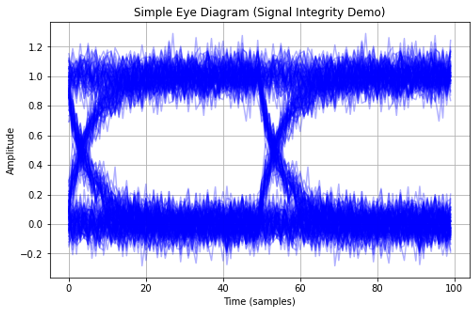
An eye diagram overlays many bits to form an eye‑shaped window. It visualizes the combined effect of attenuation, jitter, noise, and ISI.
The eye height represents voltage margin and eye width represents timing margin; crossing points reveal duty‑cycle distortion, while closure indicates high jitter or loss . Engineers use eye masks defined by standards (e.g., PCIe, USB) to check compliance.
Time‑Domain Reflectometry (TDR)
TDR instruments inject a fast step into a line and measure reflections to determine the impedance profile. The reflection coefficient ρ relates the load and line impedances, with open circuits yielding ρ = +1 and short circuits ρ = −1; matched loads have ρ = 0 . TDR reveals the location and magnitude of discontinuities such as vias, connectors, and stubs.
Frequency‑Domain S‑Parameters
S‑parameters describe how a network transmits and reflects energy as a function of frequency. Vector network analyzers (VNAs) measure S‑parameters; To characterize a 28 Gbps NRZ channel, the VNA should sweep to at least the 3rd–5th harmonic, i.e., 42–70 GHz, and VNAs provide >100 dB dynamic range compared with TDR's ~40 dB .
IBIS‑AMI and Channel Operating Margin (COM)
IBIS‑AMI models describe transmitter/receiver behavior, including equalization and clock‑data recovery (CDR). IBIS‑AMI simulation allows evaluation of voltage margin, timing analysis, jitter, eye diagrams, and COM across standards such as PCIe, USB4, and DDR.
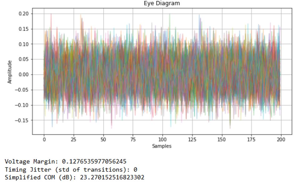
COM quantifies link margin by integrating loss, reflections, crosstalk,k, and noise into a single metric; designers compare COM results against specification thresholds to verify compliance.
High‑Speed Design Best Practices
Layer Stack‑Up and Impedance Control
Determine the number of layers, dielectric materials, and copper weights to achieve the target impedance. Use differential pairs with symmetric geometry for 100 Ω differential lines.
Avoid trace width changes and route differential pairs together to minimize skew and maintain balanced currents.
Use materials like Rogers or Megtron for 10 GHz–110 GHz signaling to reduce dielectric loss and maintain the insertion‑loss budget.
Routing Strategies
Keep high‑speed traces short and direct. Bends introduce discontinuities and additional delay. When bends are necessary, use gentle curves or 45° bends rather than 90° corners.
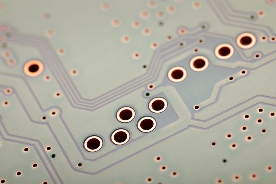
Maintain spacing and pair symmetry. Twists or unequal path lengths introduce mode conversion and skew.
Avoid crossing plane splits or voids; return currents will detour, increasing loop area and radiated emissions .
Minimize via count. For high‑speed serial lanes, use back‑drilling or blind/buried vias to remove stubs and reduce resonance. Place stitching vias near differential pair layer transitions to provide continuous return paths .
Return Path and Grounding
Solid reference planes: Provide continuous ground (and power) planes adjacent to signal layers. They act as return paths and reduce loop areas.
Controlled reference switching: When a signal changes layers, include nearby stitching vias that connect ground planes to maintain a low-inductance return path.
Separate analog and digital grounds: Partition noisy digital circuits from sensitive analog sections and join at a single point to reduce coupling.
Design Rule Checks and Simulation
Use design tools with SI/PI analysis: Layout tools can check for crosstalk, impedance, return-path, and spacing violations in real time, reducing rework.
Pre‑layout and post‑layout simulation: Use IBIS‑AMI and S‑parameter models to simulate channels, optimize equalizers, and validate COM before fabrication. Post‑layout, extract 3D models for accurate electromagnetic analysis.
Standards and Protocol Requirements
PCI Express
PCIe 6.0 adopts four‑level PAM4 modulation to double throughput. Tektronix notes that each lane delivers 64 GT/s (gigatransfers per second) and a x16 link yields 256 GB/s bandwidth . The spec sets an insertion‑loss budget of 32 dB at 16 GHz across the channel and introduces the Single‑Number Degradation Ratio (SNDR) metric for PAM4 eye quality.
Moving from NRZ to PAM4 reduces voltage spacing by 33 %, making equalization and low‑jitter clocking critical. Future PCIe 7.0 is expected to double the data rate to 128 GT/s, with 1.6 Tb/s per x16 link.
Suggested Reading: PCIe 5.0 vs 4.0: A Comprehensive Technical Deep Dive for Engineers
DDR5 and Future Memory Interfaces
The JEDEC JESD79 specification originally defined DDR5 speeds up to 6,400 MT/s (mega‑transfers per second). A 2024 JEDEC update (JESD79‑JC5) increased the maximum data rate to 8,800 MT/s, a 37.5% boost. Higher speeds reduce timing margins to the picosecond range.
Future DDR6 (under exploration) and GDDR6X/GDDR7 memory push beyond 10 Gbps per pin using multi‑level signaling and demand more stringent SI/PI budgets.
Recommended Reading: What Is GDDR6 Memory? High Bandwidth Engineering Guide & Applications 2025
USB4 and Thunderbolt
USB4 is based on the Thunderbolt protocol and scales to 80 Gbps using two‑lane operation. The USB Implementers Forum specifies that existing passive Type‑C cables support up to 40 Gbps, while new certified cables enable 80 Gbps operation. USB4 merges data and display protocols; equalization expectations are now channel‑limited, and the mechanical tolerances of Type‑C connectors add variability. Future USB4 v2 and Thunderbolt 5 may push per‑lane speeds toward 120 Gbps.
Ethernet
IEEE 802.3 continues to evolve beyond 400 GbE. The 802.3dj task force is working on 200 Gb/s per‑lane electrical signaling with 800 Gb/s and 1.6 Tb/s aggregate rates; completion is targeted for late 2026.
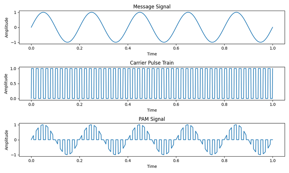
Next‑generation Ethernet will use PAM4 or higher‑order modulation and 224 G‑class electrical lanes, demanding low‑loss materials, advanced connectors, and careful de‑embedding of fixtures. High‑density cables (copper and optical) and co‑packaged optics reduce board‑level losses.
Emerging Trends and Future Challenges
Multi‑Level Modulation and 224 Gbps PAM4
As binary NRZ reaches its limits, higher‑order modulation schemes like PAM4 and PAM8 encode multiple bits per symbol.
PCIe 6.0 and 400/800 GbE already use PAM4, and future standards explore PAM6/PAM8 for 224 Gbps and beyond.
Co‑Packaged Optics and Near‑Chip Interconnects
To meet energy and density demands, next‑generation data centers adopt co‑packaged optics (CPO) and co‑packaged copper (CPC).
Optical engines are placed adjacent to the switch ASIC, eliminating long copper traces and enabling 224 Gbps and 448 Gbps links on small substrates.
Suggested Reading: What is an ASIC: A Comprehensive Guide to Understanding Application-Specific Integrated Circuits
System‑Level Channel Budgets and Measurement Plans
High‑speed success now relies heavily on explicit channel budgets, so it is important to define reach, insertion‑loss budget, number of discontinuities, and equalization strategy early in the architecture.
The measurement plan, including fixture design, S‑parameter sources, de‑embedding method,s and correlation targets, should be developed before layout. Standards like IEEE 370 guide interconnect characterization and de‑embedding practices.
Regulatory and Electromagnetic Compatibility
Product designers must meet FCC Part 15 and CISPR 32 limits on radiated and conducted emissions. Octopart highlights that return‑path design, enclosure resonances, cable, ng, and filtering influence compliance. As data rates increase, even small discontinuities can radiate; shielding, gaskets, ferrite beads, and careful cable selection become mandatory.
Suggested Reading: EMI Mitigation in High-Density Designs with Ultra-Thin Inductors and High-Current Ferrite Beads
Conclusion
Signal integrity is at the heart of high‑speed electronics. From the theoretical concept of transmission lines to the practical realities of PDN design, equalization,n, and compliance testing, every element of the system influences SI. Modern protocols – PCIe 6.0, DDR5/DDR5x, US, B4, and emerging 200-G-per-lane Ethernet – push channel bandwidths into the tens of gigahertz range. Multi‑level modulation shrinks voltage margins, while advanced packaging and co‑packaged optics shorten interconnect lengths but require rigorous characterization.
Success requires a holistic approach: early stack‑up planning, consistent impedance, well‑designed PDN, robust routing and return‑path strategies, accurate modeling with IBIS‑AMI and S‑parameters, and disciplined measurement plans. As data rates move toward 224 Gbps and beyond, SI becomes a system‑level requirement rather than a PCB afterthought.
FAQs
1. What is signal integrity,y, and why is it important?
Signal integrity refers to the preservation of a digital signal's amplitude, shape, and timing as it travels through interconnects. High‑speed signals are vulnerable to reflections, crosstalk, attenuation, jitter, and power‑supply noise. Poor SI leads to closed eye diagrams, data errors, and compliance failures . Ensuring SI is essential for the reliable operation of protocols like PCIe, DDR, and USB.
2. How does crosstalk affect high‑speed circuits?
Crosstalk occurs when electromagnetic energy couples between adjacent traces, inducing unwanted voltage on neighboring lines. It manifests as near‑end crosstalk (NEXT) and far‑end crosstalk (FEXT). Crosstalk reduces signal amplitude, introduces jitter, and increases bit‑error rate. Mitigation strategies include increasing spacing, routing differential pairs with proper coupling, shielding with ground traces, and placing return paths adjacent to signals .
3. Why are power integrity and signal integrity linked?
The power distribution network supplies current for drivers and acts as the return path for signal currents. Noise on the PDN (voltage ripple, ground bounce) modulates signal thresholds and timing, causing jitter and bit errors. Conversely, switching currents from high‑speed signals inject noise into the PDN. A low‑impedance PDN with proper decoupling is necessary to maintain both SI and PI.
4. What are eye diagrams,s and how do they help?
An eye diagram overlays multiple bits of a signal to form an "eye" pattern. It visualizes voltage and timing margins, jitter, duty‑cycle distortion, and noise. Eye height corresponds to voltage margin, while eye width corresponds to timing margin. Engineers compare eye diagrams against masks defined by standards to assess compliance.
5. How is impedance controlled on a PCB?
Impedance is controlled by trace width, dielectric thickness, dielectric constant, and reference plane placement. Using microstrip or stripline geometries with consistent dimensions yields a stable characteristic impedance (typically 50 Ω single‑ended or 100 Ω differential). Terminations (series, parallel, or AC) match the load to the line, preventing reflections.
6. Why does PCIe 6.0 use PAM4 modulation?
PCIe 6.0 doubles bandwidth relative to PCIe 5.0 by switching from NRZ (two levels) to PAM4 (four levels). Each symbol carries two bits, enabling 64 GT/s per lane and 256 GB/s on a x16 link . PAM4 reduces voltage spacing between levels, making SI more challenging; equalization and SNDR metrics are used to ensure eye quality.
References
Altium, “Introduction to high‑speed signal integrity for PCB designers,” Altium Resources, [Online]. Available: https://resources.altium.com/p/introduction-to-high-speed-signal-integrity-for-pcb-designers
Cadence, “Eye diagram analysis for high‑speed SI validation,” Cadence PCB Blog, [Online]. Available: https://resources.pcb.cadence.com/blog/eye-diagram-analysis-for-high-speed-si-validation
Ansys, “What is power integrity?,” Ansys Simulation Topics, [Online]. Available: https://www.ansys.com/simulation-topics/what-is-power-integrity
Tektronix, “PCIe 6.0 PHY validation using TDR,” Tektronix White Paper, [Online]. Available: https://www.tek.com/en/documents/whitepaper/pcie-6-phy-validation
Anritsu, “Signal integrity: S‑parameter measurements for high‑speed channels,” Anritsu Test & Measurement, [Online]. Available: https://www.anritsu.com/en-us/test-measurement/technologies/signal-integrity
Sierra Circuits, “High‑speed PCB routing best practices,” Sierra Circuits, [Online]. Available: https://www.sierracircuits.com
Protoexpress, “Best high‑speed PCB routing practices,” Protoexpress Blog, [Online]. Available: https://www.protoexpress.com/blog/best-high-speed-pcb-routing-practices/
MathWorks, “Signal integrity analysis and IBIS‑AMI modeling,” MathWorks Discovery, [Online]. Available: https://www.mathworks.com/discovery/signal-integrity.html
Design‑Reuse, “Why 6.4 Gbps DDR5 designs fail and how to avoid it,” Design‑Reuse Blog, [Online]. Available: https://www.design-reuse.com/blog/56315-why-6-4-gbps-ddr5-designs-fail-and-how-to-avoid-it/
USB Implementers Forum, “USB4 specification,” USB‑IF, [Online]. Available: https://www.usb.org/usb4
Octopart, “High‑speed standards keep raising the bar,” Octopart Blog, [Online]. Available: https://octopart.com/es/pulse/p/high-speed-standards-keep-raising-bar
HotHardware, “JEDEC DDR5 specification update,” HotHardware News, [Online]. Available:https://hothardware.com/news/jedec-ddr5-memory-huge-speed-boost-spec-update
in this article
1. Introduction2. What Is Signal Integrity?3. Key Signal Integrity Issues4. Transmission‑Line Theory and Impedance Control5. Power Integrity and Its Interaction with SI6. Signal Integrity Measurement and Analysis Techniques7. High‑Speed Design Best Practices8. Standards and Protocol Requirements9. Emerging Trends and Future Challenges10. Conclusion11. FAQs12. References