What Is GDDR6 Memory? High Bandwidth Engineering Guide & Applications 2025
Master what is GDDR6 memory with our comprehensive engineering guide covering architecture, performance formulas, design techniques and applications. Learn how dual channel architecture and 16 Gb/s per pin data rates empower GPUs, FPGAs and AI accelerators.

31 Oct, 2025. 11 minutes read
Introduction
With the development in display technologies, graphics memory has become one of the more focused industries in the global landscape. Especially with the introduction of GDDR technologies, tech enthusiasts often wonder how the latest technologies compare and what suits their needs best. So, gamers and engineers wondering what is GDDR6, and how it compares with its previous versions will find some very useful information in this article.
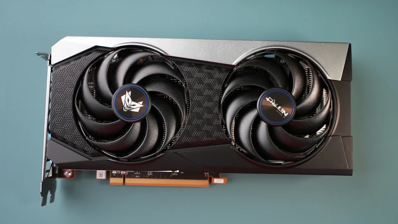
GDDR6 refers to the sixth generation of Graphics Double Data Rate (GDDR) synchronous graphics random-access memory. It is mainly used in gaming, graphics cards, and high-performance computing applications. Thanks to its low-voltage operations and speeds of up to 16GB/s, it’s a highly regarded graphics acceleration option for modern applications such as machine learning, high-resolution gaming, and professional graphics work. This article will focus on the technical foundations, architecture, and everything you need to know about GDDR6 for advanced engineering applications.
High Bandwidth GDDR6 Architecture
Modern graphics processing units (GPUs), FPGAs, and AI accelerators require memory that can quickly transfer enormous data arrays. The sixth generation of synchronous graphics RAM is called GDDR6 (Graphics Double Data Rate 6), which is in line with the JEDEC JESD250 standard.
The specification was completed in July 2017 and is focused on high-bandwidth applications such as machine learning, data-center accelerators, gaming, and automotive ADAS. While DDR4/DDR5 system memory focuses on low latency, GDDR6 prioritizes bandwidth by utilizing wide buses, quad data rate (QDR) signaling, and dual-channel architectures.
Although GDDR6 uses two separate 16-bit channels per chip, it is still synchronous dynamic RAM (SDRAM). Concurrent transactions are possible because each channel has its own clock and command/address pins. By treating a device as two separate DRAMs, the dual-channel architecture doubles concurrency, minimizes page conflicts, and simplifies controller design as compared to the single-channel GDDR5 design.
To achieve an octal data rate (ODR) for commands and a quad data rate for data, a dedicated word clock (WCK) working at up to 8 GHz is used for data transfer, while a lower frequency command clock (CK) is used for commands. The rising and falling edges of both clocks are used.
Suggested Reading: Designing Energy-Efficient AI Accelerators for Data Centers and the Intelligent Edge
Key Parameters and Signal Definitions
The JEDEC standard defines several timing and electrical parameters. Important ones include:
Data Rate/Pin (D) | Supports up to 12, 14, and 16 Gb/s. In some controllers, it can exceed 18 or even 20 Gb/s. |
Bus Width (W) | Each chip has 02 16-bit channels, and can be used in combination to form wider buses. For instance, 256-bit interfaces use eight 32-bit devices in parallel. |
Voltage Levels | Operates at 1.35 Volts and improves power efficiency as compared to GDDR5X. |
Write Clock (WCK) | Operates at half the data frequency i.e., 8 GHz for 16Gb/s. It’s internally phase-locked. |
Bus Inversions | Uses Data Bus Inversion and Command/Address Bus Inversion, which reduces switching noise. |
The peak theoretical bandwidth (B) for a memory subsystem can be calculated by:
B = D x W / 8 (GB/s)
For example, a 256‑bit wide bus using 16 Gb/s GDDR6 gives a bandwidth of:
B = 16 x 256 / 8 = 512 GB/s
Likewise, if the bus is 384 bits, the bandwidth reaches 768 GB/s. GDDR5X at 10 Gb/s on a 256‑bit bus yields 320 GB/s, a substantial advancement from the previous generations.
Recommended Reading: High Bandwidth Memory: Concepts, Architecture, and Applications
GDDR Generations Over the Years
The evolution from GDDR2 through GDDR6 brought higher clocks and wider transfers. The table below summarizes key metrics extracted from industry sources:
Generation | Memory clock | Transfer/s | Peak data rate (Gbit/s) | Bandwidth per chip (GB/s) |
GDDR2 | 500 MHz | 128 Gbit/s | 16 GB/s | 16 |
GDDR3 | 625 MHz | 2.5 GT/s | 159 Gbit/s | 19.9 |
GDDR4 | 275 MHz | 2.2 GT/s | 140.8 Gbit/s | 17.6 |
GDDR5 | 625–1000 MHz | 5–8 GT/s | 320–512 Gbit/s | 40–64 |
GDDR5X | 625–875 MHz | 10–12 GT/s | 640–896 Gbit/s | 80–112 |
GDDR6 | 875–1000 MHz | 14–16 GT/s | 896–1024 Gbit/s | 112–128 |
The key observation from this table is that GDDR6 has double the data rate of GDDR5X.
Suggested Reading: GDDR6 vs GDDR6X: A Comprehensive Technical Comparison for Digital Design & Hardware Engineers
Memory Density and Capacity
GDDR6 devices support from 8Gb to 16Gb as each channel exists per chip. So, two 16Gb devices can work in the clamshell mode to provide compatibility for 32-bit interfaces. Therefore, it supports high-density applications like Nvidia’s RTX 2080 Ti commercial graphics cards.
Command Protocol and Timing
In GDDR6, there are separate command clocks (CK) and write clocks (WCK).
Command clock runs at 2GHz.
Word Clock runs at up to 8GHz.
Thanks to the double data rate, it produces a transfer rate of 16 Gb/s per pin. Since commands and data are latched on rising and falling edges, it amplifies data transfer.
Physical Considerations
The following table summarizes the electrical and physical considerations for GDDR6:
Package | 180-ball FBGA package with 14 mm footprint |
Voltage Rails | Separate Vdd and Vddq rails that require PCB decoupling. |
Thermal Properties | Dissipates substantial heat, so it requires heat spreaders and controlled impedance traces. |
Analysis and Design Techniques
For efficient designs involving GDDR6, engineers must consider aspects like bandwidth requirements, bus widths, design controllers, and signal integrity. Here are some useful ways for a quantitative analysis:
Start with Bandwidth and Latency
For accelerator units and GPUs, it is important to estimate the data throughput. For instance, a gaming pipeline of 4K/120Hz may generate a framebuffer traffic of around 132GB/s.
Set the Number of Channels and Bus Width
The bus width can be calculated with the formula discussed earlier. As an example, if you need 512Gb/s and you have 16 Gb/s chips available, the formula will yield that a 256-bit interface will be enough.
The Achronix Speedster7t1500 FPGA contains 08 GDDR6 subsystems, where each provides 512Gb/s, delivering a total of 4Tb/s.
Determine Required Memory Density
To achieve the capacity requirements, simply multiply the per-chip capacity (either 8 Gb or 16 Gb) by the number of devices. So, if you need 08 2-Gb devices to extract 16 Gb.
Controller IP and PHY Considerations
Pick a controller that supports JESD2508B and your desired target speed. Moreover, focus on the PHY interface. It must be similar to DFI 5.0 with an 8:1 frequency ratio.
Calculate Your Power Budget
Calculate the estimated switching power by the formula:

Here, C is the load capacitance, V is the voltage and f is the switching frequency.
Signal Integrity Simulations
Signal integrity is a major problem at high data rates of 16Gb/s. Slight mismatch in impedances and trace discontinuity can lead to intense jitter. Therefore, it is a good idea to perform simulations using the IBIS-AMI models. Also, verify the eye diagrams. While designing PCBs, it’s a good idea to use short stub lengths, equal trace lengths across the WCK and DQ nets. Moreover, target 50 Ω single-ended and 100 Ω differential pairs.
Suggested Reading: How to Design a PCB Layout: A Comprehensive Guide
Training and Initialization
GDDR6 requires ZQ calibration, WCK training, and sequences for read/write delays. In most modern controllers, these processes can be automated.
In-System Validation
Use built-in-self-test (BIST), ECC features, and error injection to evaluate your system and its reliability. Achronix and Cadence provide high-quality test bench tools for simplified verification.
Example: Calculating Throughput and Latency
The following Python snippet show how to compute bandwidth and approximate frame buffer latency. For instance, if an accelerator uses a 16 Gb/s per‑pin device on a 256‑bit bus. Each frame is 50 MB. How long does it take to transfer one frame? Here is how to calculate.
# Parameters
per_pin_rate = 16e9      # 16 Gb/s per pin
bus_width_bits = 256     # total bus width
frame_size_bytes = 50e6  # 50 MB per frame
# Compute bandwidth
bandwidth_bytes_per_sec = per_pin_rate * bus_width_bits / 8
transfer_time_sec = frame_size_bytes / bandwidth_bytes_per_sec
print(f"Theoretical bandwidth: {bandwidth_bytes_per_sec/1e9:.2f} GB/s")
print(f"Frame transfer time: {transfer_time_sec*1e6:.2f} microseconds")
The code shall yield a bandwidth of approximately 512 GB/s and 97us per 50 MB frame. These parameters are generally used for design budgeting.
Common GDDR6 Applications
Professional Graphics and Gaming
GDDR6 has regular applications in graphics processing, high‑resolution gaming, and virtual reality. For instance, Nvidia’s GeForce RTX 2080 TI ship can achieve a 616GB/s bandwidth with 11GB of GDDDR6.
As a result, there is smooth gameplay in 4K/60Hz and complex shaders. Moreover, next generation console devices like Xbox Series X feature 16 GB GDDR6 that enables unified memory for CPU and GPU. Likewise, the Sony PS5 features a GDDR6 for cost-effective performance.
High‑Performance Computing (HPC)
High performance computing requires high data throughput. Generally, it’s a problem with traditional DDR as they cannot feed thousands of GPU cores. But thanks to GDDR6, there is a cost-friendly option to avail HBM as these memory units can deliver hundreds of GBs per second at a much lower cost.
FPGA boards like Achronix Speedster 7t feature eight GDDR6 subsystems that can provide up to 4Tbps bandwidth and support real time analytics and streaming applications. Hence, GDDR6 becomes a viable option for scientific applications, simulations and financial computing.
Suggested Reading: Breakthroughs in Quantum Computing
Artificial Intelligence and Machine Learning
Since AI and machine learning involve matrix multiplication, it puts an enormous load on the memory bandwidth. In Artificial Intelligence, HPC and cryptocurrency mining, large volumes of data and video are generated which require high memory bandwidth.
With GDDR6 allowing up to 16 to 20 Gb/s per pin, it’s a viable option for AI accelerators to sustain high throughput at an optimal price.
Networking and Data Centers
In order to perform deep packet inspection and buffer packets, next-generation routers and network interface cards (NICs) need memory bandwidth. The 16 Gb/s per-pin rate of GDDR6 is compatible with 400 Gb/s and 800 Gb/s networking equipment.
Automotive and Embedded Systems
Autonomous vehicles and advanced driver-assistance systems (ADAS) process high-resolution sensor data in real time. GDDR6 satisfies automotive temperature and reliability requirements while offering the required bandwidth.
Its dual-channel architecture makes integrating with heterogeneous SoCs with safety processors, AI engines, and GPU cores easier.
Suggested Reading: ADAS and the Road to Autonomous Driving: Insights from Nexperia's Industry Expert Ahad Buksh
Integration with FPGAs, GPUs and emerging technologies enables scalable systems
GDDR6 does not operate in isolation; its integration with compute units determines real‑world performance.
Integration with FPGAs
GDDR6 integration with modern FPGA boards is one of the ways forward in digital design and fabrication. For instance, the Achronix Speedster7t family tightly integrates with GDDR6, where each subsystem includes a controller, PHY and interfaces to a network‑on‑chip (NoC).
The 256-bit AXI4 interface allows these subsystems to connect to the FPGA fabric. Moreover, they can connect directly, using 512‑bit AXI4. As a result, the architecture allows independent operation of dual channels and is supported by‑16 or by‑8 clamshell modes.
It allows designers to choose either NoC or direct connections depending on latency and throughput requirements.
Integration with GPUs and SoCs
GPUs embed multiple memory controllers that interface with GDDR6 devices. These dual‑channel architectures reduce address conflicts. Moreover, they support high concurrency, due to which, manufacturers can implement 256‑ or 384‑bit buses connecting to multiple 16‑Gb devices.
For GPUs and SoCs, the command and word clocks must be phase‑aligned across all devices. SoC designers integrate the GDDR6 controller into the chip’s memory subsystem via DFI 5.0‑like interfaces with an 8:1 frequency ratio to ease timing closure.
Compatibility with Other Memory Technologies
GDDR6 delivers high bandwidth at moderate cost, so it competes with HBM2/3 and LPDDR5/6. On the other hand, HBM offers higher bandwidth per package (>1 TB/s) with a wider, stacked bus but at significant cost and packaging complexity. Likewise, LPDDR caters to mobile devices focusing on low power.
The advantage of GDDR6 is that it lies between these extremes, so it balances bandwidth, cost and power. Hybrid systems may combine GDDR6 for main memory with on‑chip caches and HBM for scratchpad storage.
Moreover, emerging Compute Express Link (CXL) lets GDDR6 memory modules to be shared across accelerators, expanding its role in disaggregated architectures.
Suggested Reading: What is High Bandwidth Memory 3 (HBM3): Complete Engineering Guide 2025
Common Integration and Implementation Pitfalls and their Solutions
Integrating GDDR6 with FPGA and GPUs can often bring challenges. Here is a quick look at the common issues and their solutions.
Issue | Description | Solution |
Clock Skew between CK and WCK | At high speeds of 16Gb/s, a minor skew of just 10ps can lead to timing mismatches | Using matched-length traces and dedicated phase-locked loops can improve performance. |
Noise and Signal Integrity | Due to rapid edges and high data rates, the crosstalk can increase substantially. | CABI and DBI reduce simultaneous switching. Moreover, maintaining impedance, proper termination and reduced vias help in reducing noise. |
Power Rail Noise | Poor regulation in VDD and VDDQ can occur due to separate rails | Using low noise regulators reduce rail noise. |
Advanced Techniques for GDDR6 Implementation
Thanks to advanced engineering techniques, GDDR6 no longer remains only a memory interfacing unit. Here are a few tips to know.
Split Channel operation and clamshell mode allows two devices to share the same address bus but separate data buses. It increases capacity without needing additional bus width. Designs can power down one half to save power during light workloads.
Memory Acceleration with GDDR6‑AiM uses tiny processing engines inside each memory bank. It helps in offloading operations like vector dot products or activation functions. Eventually, it reduces data movement and improves energy efficiency. It’s an emerging area where engineers can experiment with algorithms that map computations into memory.
Dynamic frequency and voltage scaling (DVFS) in some GDDR6 controllers allow runtime adjustment of WCK and CK frequencies. It reduces frequency during idle periods and lowers power consumption. Combining DVFS with clock gating and DBI yields significant energy savings.
Multi‑channel interleaving and striping is an advanced technique allowing data distribution across multiple GDDR6 subsystems (interleaving). It reduces bursty traffic and hides latency. For example, splitting a data stream across four 512 Gbps channels increases concurrency and reduces bank conflicts.
Further Reading: HBM2 vs GDDR6: Engineering Deep Dive into High-Performance Memory Technologies
Conclusion
GDDR6 is an evolutionary breakthrough in graphics processing and high bandwidth memory applications. It combines a dual channel architecture with quad data rate signaling and consumes less voltage, delivering up to 16 Gb/s per pin. It can deliver double the throughput of its predecessor.
This article discussed the technical foundations, design methodologies, industry applications and future trends of GDDR6 memory. It will allow engineers to apply formulas to calculate required bus width, leverage robust controllers and PHY IP, and employ best practices to mitigate signal‑integrity and power challenges. Modern FPGAs and GPUs scale bandwidth into the terabit‑per‑second range using multiple GDDR6 subsystems, enabling innovation across gaming, AI, HPC and automotive domains.
In the future, GDDR6X and GDDR6W push per‑pin speeds beyond 20 Gb/s, while processing‑in‑memory technologies embed compute logic directly into GDDR6 packages. By the late 2020s, GDDR7, chiplet‑based architectures and memory disaggregation via CXL may redefine high‑bandwidth design paradigms. Awareness of latest standards, leveraging advanced tools and embracing innovative architectures will allow engineers to harness the full potential of GDDR6 and its successors.
Frequently Asked Questions (FAQs)
What is GDDR6 memory and how is it different from DDR4?
GDDR6 is a type of synchronous graphics RAM designed for high‑bandwidth workloads. DDR4 prioritizes low latency for CPU applications, but GDDR6 uses wide buses, dual‑channel architecture and quad data rate signaling to deliver up to 16 Gb/s per pin. It operates at 1.35 V and is used in GPUs, FPGAs and AI accelerators rather than as system memory.
How does GDDR6 achieve higher bandwidth than GDDR5?
GDDR6 achieves high bandwidths by doubling the number of data transfers per clock cycle relative to GDDR5 and introduces a dual‑channel architecture with two 16‑bit channels per chip. Also, it increases the write clock to 8 GHz and uses separate command and data clocks. These changes raise per‑pin data rates to 12–16 Gb/s compared with GDDR5’s 8 Gb/s.
What are the power advantages of GDDR6?
GDDR6 uses bus inversion and lowered core voltages, which reduces dynamic power. It also supports dynamic frequency scaling and power‑down modes through controller IP. However, absolute power consumption still depends on bandwidth utilization; high‑performance GPUs may require robust cooling.
Can I use GDDR6 for AI workloads instead of HBM?
Yes. For many inference and mid‑range training workloads, GDDR6 provides sufficient bandwidth at lower cost. Each chip can deliver 112–128 GB/s, and multi‑channel systems can scale to several terabytes per second. HBM offers higher bandwidth per package but carries higher costs and packaging complexity. Choose based on your bandwidth and budget requirements.
What is the difference between GDDR6X and GDDR6W?
GDDR6X uses PAM4 signaling to push per‑pin bandwidth to 19–21 Gb/s. It consumes less power per bit transferred but overall power increases due to speed. GDDR6W, announced in 2022, doubles I/O pins to 64 and uses FOWLP packaging, enabling 22 Gb/s per pin and doubling capacity to 32 Gb. GDDR6X focuses on signaling innovation, while GDDR6W focuses on packaging and capacity.
References
- M. Jennings, "GDDR6 Memory explained: What it is, and why it matters," GamesRadar, https://www.gamesradar.com/gddr6-memory-explained/
- "GDDR6 SDRAM," Wikipedia, https://en.wikipedia.org/w/index.php
- Achronix, "Speedster7t GDDR6 User Guide," https://www.achronix.com/sites/default/files/docs/Speedster7t_GDDR6_User_Guide_UG091.pdf
- Cadence Design Systems, "Denali Controller IP for GDDR6," https://www.cadence.com/content/dam/cadence-www/global/en_US/documents/tools/silicon-solutions/protocol-ip/denali-controller-ip-gddr6-br.pdf
- "GDDR Memory Advantages and Disadvantages," RF Wireless World, https://www.rfwireless-world.com/terminology/gddr-memory-advantages-disadvantages
in this article
1. Introduction2. High Bandwidth GDDR6 Architecture 3. Analysis and Design Techniques4. Common GDDR6 Applications5. Integration with FPGAs, GPUs and emerging technologies enables scalable systems6. Advanced Techniques for GDDR6 Implementation7. Conclusion8. Frequently Asked Questions (FAQs)9. References