EMI Mitigation in High-Density Designs with Ultra-Thin Inductors and High-Current Ferrite Beads
Explore how ultra-thin inductors and high-current ferrite beads deliver superior EMI mitigation, power efficiency, and reliability in high-density, high-frequency electronic designs.

11 Nov, 2025. 5 minutes read
Electronics broadly are moving toward higher bandwidth, lower latency, and denser system integration. High-speed interconnects such as PCIe Gen 5/6, multi-lane Ethernet, and AI accelerators now sit at the center of servers and compute platforms. Alongside these advances, power delivery networks have become more sophisticated, with Integrated Voltage Regulators (IVRs) switching anywhere from 2 MHz to 100 MHz to optimize efficiency and transient response.
While these changes deliver performance benefits, they also amplify electromagnetic interference (EMI) challenges. As dies, power stages, and interconnects are packed into increasingly compact footprints, the EMI margin available to designers shrinks. Power integrity and signal integrity are closely coupled, and even small increases in ripple or noise can degrade system-level compliance.
The switch from discrete passives to co-packaged and embedded components means that inductors and ferrite beads are integral to the overall architecture. Namely, their selection directly impacts regulatory compliance, overall efficiency, and thermal headroom. As such, engineers now face the task of choosing components that meet performance specifications and maintain EMI control without compromising form factor or power density.
EMI Sources and Their Impact on System Design
EMI in modern electronics stems from multiple sources, but power delivery noise and signal path coupling are arguably the two most prominent.
Power delivery noise arises in DC/DC converters and IVRs, where high dI/dt transitions drive ripple into sensitive power rails. As switching frequencies climb toward tens of megahertz, the harmonic spectrum broadens and pushes more noise into bands where it can couple into critical signals.
Signal path noise coupling is especially prominent in server motherboards. Devices like PCIe re-timers, Ethernet controllers, and switch ASICs operate close to emission compliance limits and rely on stable supply rails to maintain signal integrity. Without effective suppression, conducted EMI from the power delivery network can migrate into these ICs, degrade link stability, and increase error rates.
Generally speaking, EMI can manifest as either conducted interference, traveling through rails and interconnects, or radiated emissions, emanating from traces, packages, and cables. Both impact compliance and system function. For example, in GPU and AI accelerator subsystems, inadequate EMI control at the power entry point can result in corrupted data transfer and reduced throughput.
Complicating matters further, regulatory compliance pressures continue to increase. Engineers must deliver systems that pass tight EMI testing without sacrificing board density or introducing excessive power losses. This demands a component-level strategy where inductors and beads are selected based on both electrical and mechanical performance.
Ultra-Thin Inductors for High-Frequency IVRs
As switching frequencies in IVRs approach 100 MHz, inductance requirements shift downward, and package constraints dictate smaller case sizes. Traditional wire-wound inductors cannot always scale to these requirements, leading to the adoption of thin-film inductors optimized for high-FSW applications.
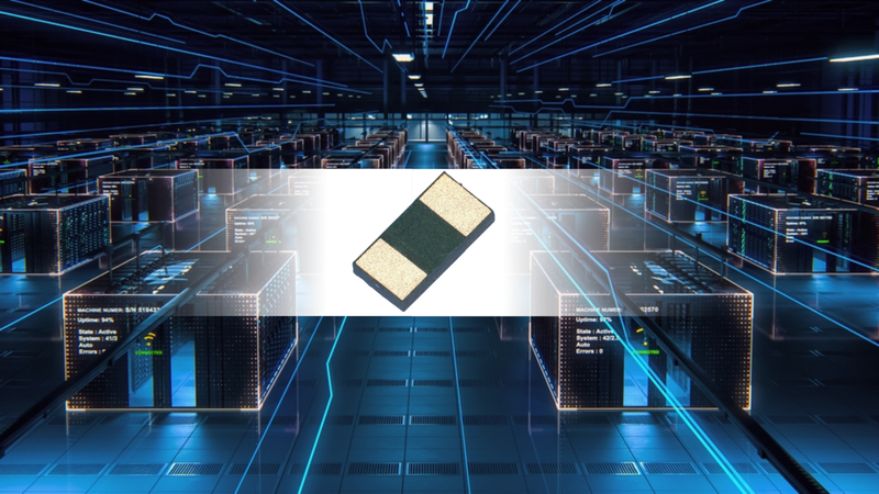
Mounting strategies are therefore instrumental to minimizing EMI. Ultra-thin inductors can be placed die-side, land-side, or embedded within the interposer, and these placements enhance current level transient speed by reducing loop area and parasitics. Murata’s ultra-thin solutions are available in footprints as small as 0402 (1.0 x 0.5 mm) and 0603 (1.6 x 0.8 mm), with single devices and array options for multi-phase regulator designs.
Beyond size reduction, these inductors offer the benefit of a low-profile form factor that enables mechanical integration without increasing z-height in stacked-die or co-packaged environments. Placement flexibility also helps balance thermal hotspots, thereby improving overall reliability.
Customization is another strong suit. Murata’s UTL series enables the tuning of inductance, DCR, and footprint to match the specific requirements of each package VR, ensuring that inductors integrate cohesively with both the electrical demands of the IVR and the mechanical limitations of the package. Ultimately, by reducing EMI at the source, these inductors improve regulator efficiency, maintain compliance margins, and support the continued scaling of high-frequency IVRs.
Ferrite Beads as Power Rail Filters in High-Current Circuits
Where inductors address EMI at the switching node, ferrite beads are essential in filtering noise on the power rails themselves. Their function is to present high impedance at noise frequencies while maintaining low DC resistance (DCR) to minimize voltage drop in high-current paths.
The parameters of Murata’s ferrite bead families illustrate this balance.
The BLM18SP series (0603) achieves current ratings of up to 3.7 A at 85 °C, with a DCR as low as 0.022 Ω, while offering impedance values of up to 1000 Ω at 100 MHz.
The BLM21SP series (0805) supports up to 2.8 A at 85 °C with a maximum DCR of 0.04 Ω
For extreme high-current environments, the BLM31SN and BLE32 series extend this performance.
The BLE32SN120 ferrite bead supports 20 A at 85 °C with a DCR of 0.0006 Ω, providing EMI suppression without significant IR drop.
These specifications directly translate into system-level benefits. On server motherboards, PCIe re-timer ICs often require rail filtering to prevent supply noise from coupling into signal paths. Similarly, beads can isolate noise between CPU, NIC, and GPU rails without affecting transient response.
Performance stability under load is also vital. The BLE32SN120 maintains an impedance of over 25 Ω even at a DC bias of 5 A to guarantee consistent attenuation across varying load conditions. For engineers, this stability reduces the risk of noise leakage under real-world operating currents.
The trade-offs lie in bead size and impedance selection. Higher impedance improves noise attenuation but can increase insertion loss, while lower DCR reduces voltage drop at the expense of filtering effectiveness. Murata’s broad portfolio provides flexibility to balance these trade-offs according to system needs.
Matching Component Architecture to EMI Profiles
EMI suppression is not achieved by a single component but through a matched architecture of inductors and beads. Each has a distinct purpose in addressing different points of noise generation and coupling.
For high-Fsw IVRs, ultra-thin inductors mounted close to the load reduce switching loop parasitics and enhance current level transient speed. Meanwhile, ferrite beads placed between the regulator output and load isolate sensitive devices from conducted noise on shared rails.
Co-design considerations are equally important. Embedded inductors free surface board space, allowing beads to be placed closer to load pins where they are most effective. Low-DCR beads, such as those in the BLE32 series, prevent excessive IR drop in multi-rail, high-current environments typical of data center and networking hardware.
A practical example is a server NIC. Here, a land-side UTL inductor can serve the VRM, while a BLM31SN bead filters the supply rail feeding the NIC. This pairing offers a path toward EMI compliance without requiring oversized passives that consume board space and minimize efficiency.
Designing for Future EMI Requirements
The next generation of electronics will push EMI challenges even further. Switching currents are rising, frequencies are accelerating, and packaging density continues to increase. These shifts heighten the risk of EMI coupling across rails, traces, and interconnects.
Mitigation strategies must therefore start early. Selecting thin-film inductors and high-current beads during initial design phases reduces the likelihood of compliance failures that can trigger costly redesigns. Customization is central to this approach. By tailoring parameters such as inductance, impedance, and DCR, engineers can align component behavior with changing rail specifications and transient response needs.
Collaboration between system designers and component suppliers will also be necessary. Predictive EMI mitigation, where solutions are co-optimized in advance of full integration, means that compliance can be achieved without compromising performance or density. Such a proactive approach is tangential to industry trends toward co-packaging and heterogeneous integration, where component choices directly shape system outcomes.
Conclusion
With system performance hinging on both compliance and efficiency, engineers require components that address noise at multiple levels.
By providing engineers with a broad portfolio of customizable inductors and beads, Murata unlocks designs that meet today’s standards and anticipate tomorrow’s challenges. For systems ranging from servers to AI accelerators, these components make balancing EMI, efficiency, and mechanical integration a reality.