PCIe 5.0 vs 4.0: A Comprehensive Technical Deep Dive for Engineers
Unpacking the architectural advancements, performance gains, and practical considerations of the latest PCIe generations for technical professionals.

03 Jun, 2025. 17 minutes read
Key Takeaways:
PCIe 5.0 doubles PCIe 4.0's raw data rate to 32 GT/s per lane, yielding 128 GB/s bidirectional bandwidth on an x16 link for data-intensive tasks.
Achieving PCIe 5.0 speeds requires significant physical layer enhancements, such as advanced equalization, mandatory precoding, and a tighter -36dB channel loss budget, which introduces design and validation hurdles.
PCIe 5.0 primarily evolves the physical layer while maintaining 128b/130b encoding and backward compatibility, building upon the features of PCIe 4.0, such as extended tags and credits.
PCIe 5.0 offers the most significant benefits for next-gen NVMe SSDs, high-speed networking (400GE+), and AI/ML accelerators, with current gaming GPUs seeing smaller gains.
The maturing PCIe 5.0 ecosystem demands that engineers consider thermal management, PCB design, and signal integrity solutions like retimers for robust implementations.
PCIe 5.0 vs 4.0: Understanding the Generational Leap in High-Speed Interconnects
Data generation and processing have expanded exponentially across diverse computing landscapes. including:
Artificial Intelligence (AI)
Cloud infrastructure
Immersive gaming
To sustain these applications, there is an intense and continuous demand for higher Input/Output ( I/O) bandwidth. Hence, interconnect technologies like Peripheral Component Interconnect Express (PCIe) are critical in preventing system performance from being throttled by data bottlenecks. This article focuses on the pivotal comparison of PCIe 5.0 vs 4.0, highlighting the advancements and implications for engineers.
Recommended Reading: Improved electrical interconnects for data centers with higher-power delivery and smaller-footprint
What is PCIe?
PCIe (Peripheral Component Interconnect Express) is a high-speed connection that links different hardware parts inside a computer. It has significantly evolved, establishing itself as the de facto high-speed peripheral interface standard. The PCI Special Interest Group (PCI-SIG) is responsible for defining and managing these open industry standards, ensuring interoperability and a robust ecosystem.
The progression from PCIe 4.0 to PCIe 5.0, and subsequently to PCIe 6.0, highlights the increasing capabilities in terms of bandwidth. This pace of development may even exceed the immediate requirements of more traditional consumer applications, suggesting that the PCIe roadmap is heavily influenced by the demands of specialized, high-growth compute domains.
PCIe 5.0 vs 4.0 - Core Specifications
Understanding the fundamental data transfer capabilities and encoding schemes of PCIe 4.0 and PCIe 5.0 is essential before delving into more granular architectural details. This section discusses these core specifications.
PCIe 4.0: Setting the Stage
PCIe 4.0 marked a significant advancement in interface speed, officially introduced by the PCI-SIG with its revision 0.9 specification announced in June 2017. This generation doubled the performance of its predecessor, PCIe 3.0.
PCIe 4 focused on overall system efficiency and manageability. Hence, its key performance metrics include:
A data rate of 16 GT/s (2 GB/s unidirectional) per lane, meaning an x16 slot provides 32 GB/s unidirectional or 64 GB/s bidirectional bandwidth.
PCIe 4.0, like PCIe 3.0, uses the efficient 128b/130b encoding scheme, which has a low 1.54% overhead for maximum usable bandwidth.
Beyond raw speed, PCIe 4.0 introduced key enhancements, including:
Extended tags/credits for latency masking
Reduced system latency
Lane margining for link health
Improved RAS features
Scalability
Improved I/O virtualization/platform integration.
PCIe 5.0: Doubling Down on Speed
The development of PCIe 5.0 was notably rapid, with the PCI-SIG publishing the version 0.9 specification in late 2018 or early 2019. The final specification release came in in May 2019, less than two years after the finalization of PCIe 4.0. It highlighted the pressing need for even greater bandwidth in certain industry segments.
The PCIe 5.0 focused on innovation around the PHY level. Its key performance metrics include:
Doubled data rate of PCIe 4.0, achieving 32 GT/s per lane, translating to a unidirectional bandwidth of approximately 4 GB/s per lane. For an x16 slot, this means a unidirectional bandwidth of about 64 GB/s, or a substantial 128 GB/s in a bidirectional configuration.
PCIe 5.0 retains the 128b/130b encoding, but its doubled bandwidth for AI, high-speed networking, and advanced storage significantly stresses the physical layer. It forced major electrical changes to ensure signal integrity, all while maintaining backward compatibility and low power consumption.
With consistent 128b/130b encoding across PCIe 3.0 to 5.0, each generation's doubled data rate (e.g., PCIe 4.0's 8 GT/s to PCIe 5.0's 16 GT/s) shifts the engineering challenge to the physical layer, demanding a doubling of raw signaling frequency.
To deal with signal degradation in higher frequencies, PCIe 5.0 specification emphasizes major aspects of signal integrity, including:
Significant electrical changes
Advanced equalization
Precoding
Tighter budgets for jitter and channel loss
Suggested Reading: Decoupling Capacitors: Mastering Power Integrity in Electronic Design
PCIe 4.0 vs. PCIe 5.0 - Key Specification Comparison
To provide a clear, side-by-side view of their core attributes, the following table summarizes the key specifications for PCIe 4.0 and PCIe 5.0. This allows for a quick understanding of the quantitative differences and the scale of advancement between these two generations.
Parameter | PCIe 4.0 | PCIe 5.0 |
Data Rate per lane (GT/s) | 16 | 32 |
Frequency (GHz) | 8 (NRZ) | 16 (NRZ) |
Encoding | 128b/130b | 128b/130b |
Encoding Overhead (%) | ~1.54 | ~1.54 |
Effective Bandwidth per lane (GB/s, unidirectional) | ~1.969 (16 GT/s * (128/130) / 8) | ~3.938 (32 GT/s * (128/130) / 8) |
Max Bandwidth x1 (GB/s, bidirectional) | ~3.94 | ~7.88 |
Max Bandwidth x4 (GB/s, bidirectional) | ~15.75 | ~31.50 |
Max Bandwidth x8 (GB/s, bidirectional) | ~31.50 | ~63.01 |
Max Bandwidth x16 (GB/s, bidirectional) | ~63.01 | ~126.03 |
Channel Insertion Loss Budget (dB) | -28 dB @ 8 GHz | -36 dB @ 16 GHz |
Bit Error Rate (BER) Target | 10−12 | 10−12 |
Architectural Evolution: A Layer-by-Layer Analysis of PCIe 5.0 vs 4.0
The PCIe architecture is structured in layers:
Physical Layer
Data Link Layer
Transaction Layer
To fully appreciate the advancements in PCIe 5.0 over PCIe 4.0, it is essential to examine the changes and enhancements within each of these layers.
Physical Layer (PHY) Advancements in PCIe 5.0
The Physical Layer (PHY) is perhaps the biggest point of difference between PCIe 5.0 and PCIe 4.0. This is due to the doubling of the data rate to 32 GT/s. The main challenge at this layer is to maintain signal integrity, ensuring reliable data transmission at these higher speeds, often over existing or slightly improved channel materials.
Signal Integrity Challenges at 32 GT/s and Solutions
PCIe 5.0's 32 GT/s data rate pushes the Nyquist frequency to 16 GHz, leading to significantly increased signal loss across PCB traces, connectors, and component packages. It therefore requires a -36 dB total channel insertion loss budget at 16 GHz, tighter than PCIe 4.0's -28 dB at 8 GHz. This demands precise management of signal degradation like reflections, crosstalk, and mode conversion.
Like its predecessor, PCIe 5.0 utilizes Non-Return-to-Zero (NRZ) signaling, a key difference from PCIe 6.0's move to PAM4. To handle 32 GT/s NRZ, PCIe 5.0 implements specific electrical changes to enhance signal integrity and bolster connector mechanical performance. The Card Electromechanical (CEM) connector, for example, maintains backward compatibility while accommodating these higher speeds.
Suggested Reading: PCBA Signal Integrity Problems: Ten Factors to Consider
Equalization Enhancements: PCIe 5.0 vs. 4.0
Equalization is a critical technique used to compensate for channel-induced signal degradation effectively "opening" the signal eye at the receiver, such as Continuous Time Linear Equalization (CTLE) and Decision Feedback Equalization (DFE).
PCIe 4.0, operating at 16 GT/s, is already considered a "closed-eye" specification, meaning the signal eye is often closed at the receiver before equalization due to inter-symbol interference. Thus, a robust receiver equalization strategy is vital for PCIe 4.0.PCIe 5.0 also mandates 500-nanosecond TXEQ in-band handshaking during link training, resulting in an extremely small post-equalization eye height of 10- 15 mV and an eye width of around 9.375 picoseconds. It involves a 3-tap DFE and a 2nd-order CTLE.
The Role of Precoding in PCIe 5.0
Precoding is a significant new feature mandated for PCIe 5.0 transmitters operating at 32 GT/s, if requested by the link partner during link training. This feature was not present in the PCIe 4.0 specification.
Precoding handles the impact of burst errors, particularly those that can be introduced by the DFE circuitry in the receiver. A DFE uses past decisions about received bits to cancel out ISI from those bits. However, if a DFE makes an incorrect decision, this error can propagate, leading to a burst of subsequent errors. Precoding helps to break such error bursts into two distinct, smaller errors: an entry error and an exit error.
Clock Jitter Specifications and Reference Clock
Maintaining precise timing is crucial at high data rates. PCIe 5.0 specifies a significantly tighter reference clock Root Mean Square (RMS) jitter of 0.15 picoseconds (ps), compared to 0.5 ps RMS for PCIe 4.0.
Some documentation also indicates a 0.25 ps RMS design requirement for the PCIe 5.0 reference clock. These stricter jitter requirements are essential for preserving timing margins at 32 GT/s. Like PCIe 4.0 and 3.0, PCIe 5.0 supports various clocking architectures, including common clock, separate reference clock with no spread (SRNS), and separate reference clock with spread spectrum clocking (SRIS).
Suggested Reading: Clock Gating: Powering Down Idle Circuits
Link Training (LTSSM), Speed Negotiation, and Ordered Sets
The Link Training and Status State Machine (LTSSM) is a fundamental part of the PCIe PHY, responsible for configuring the link, including negotiating link width, operational speed, and equalization settings with the link partner.
Achieving PCIe 5.0's 32 GT/s requires a progressive link equalization process. The link incrementally trains, starting at 2.5 GT/s, then negotiating up through PCIe Gen3 (8 GT/s), Gen4 (16 GT/s), and finally to Gen5 (32 GT/s), with equalization adjustments at each stage.
PCIe 5.0 updates specific Ordered Sets for link management, including Electrical Idle Exit Ordered Sets (EIEOS) and SKP Ordered Sets. EIEOS transitions the link from electrical idle. SKP Ordered Sets periodically compensate for clock frequency differences between linked devices, preventing buffer issues.
Retimers vs. Redrivers: Ensuring Signal Reach
As signal speeds rise, retimers become vital for maintaining signal integrity over longer PCIe channels. Unlike redrivers, which only amplify signals (and noise), retimers actively recover and retransmit a clean signal, participating in the PCIe protocol and resetting jitter/insertion loss budgets.
For PCIe 5.0, retimers are even more critical. They uniquely support 32 GT/s precoding and lane margining. While redrivers offer limited use for very short extensions, retimers are strongly preferred for reliable PCIe 4.0 and 5.0 operation, especially in complex systems with extended traces or multiple connectors.
Data Link Layer (DLL) Developments
The Data Link Layer (DLL) in PCIe architecture is responsible for ensuring reliable data transfer between two directly connected components. Its key functions include managing link-level error detection and correction (e.g., via LCRC and sequence numbers) and implementing flow control.
Flow Control Mechanisms
PCIe uses a credit-based flow control system, operating per Virtual Channel (VC), to prevent receiver buffer overflows. Receivers advertise available buffer space for different Transaction Layer Packet (TLP) types:
Posted (P)
Non-Posted (NP)
Completions (Cpl).
There are separate credits for TLP headers (PH, NPH, CPLH) and data payloads (PD, NPD, CPLD).
Flow Control Initialization (FC_INIT) DLLPs exchange initial buffer sizes. As receivers process TLPs and free space, they send FC_Update DLLPs to return credits, allowing more TLPs. This core credit-based flow control remains consistent between PCIe 4.0 and PCIe 5.0 for non-FLIT mode, leveraging PCIe 4.0's robust foundation.
Enhancements in Scaled Flow Management
Scaled Flow Management is a key advantage carried over from PCIe 4.0 to PCIe 5.0. This feature allows flow control credits to be managed in larger units, significantly reducing the frequency of FC_Update DLLPs. At higher data rates, this lowers flow control overhead, making the process more efficient.
The core credit-based flow control mechanism for non-FLIT mode remains consistent between PCIe 4.0 and 5.0. This stability shows that earlier PCIe generations were robustly designed with foresight. This effective architectural layering allowed PCIe 5.0 development to focus heavily on the demanding Physical Layer innovations needed for its raw speed increase.
Transaction Layer (TLL) Refinements
The Transaction Layer (TLL) is the uppermost layer in the PCIe protocol stack. It is responsible for generating and receiving Transaction Layer Packets (TLPs), which are used to communicate requests and data between PCIe devices.
Extended Tags and Credits
PCIe 4.0 introduced extended tags and credits, crucial for masking latency and maximizing bandwidth, a feature continued in PCIe 5.0. Traditionally, a TLP header's 8-bit "Tag" field allowed 256 unique outstanding Non-Posted Requests. Extended Tags significantly expand this, enabling many more concurrent requests. This enhancement is vital for high-performance devices like NVMe SSDs and modern NICs, which demand deep command queues and parallelism to achieve high throughput.
Without it, raw bandwidth increases alone wouldn't fully utilize the link. Extended tags ensure the protocol can support the increased concurrency needed for I/O-intensive workloads, complementing the Physical Layer's speed gains.
Performance, Power, and Practicality: PCIe 5.0 vs 4.0
This section examines the tangible outcomes for engineers:
- Performance improvements
- Power consumption characteristics
- Real-world usability aspects when comparing PCIe 5.0 and PCIe 4.0.
Bandwidth and Throughput: Theoretical vs. Real-World Gains
The most prominent difference between PCIe 5.0 and PCIe 4.0 is the doubling of theoretical bandwidth.
A PCIe 4.0 x16 link offers approximately 64 GB/s of bidirectional bandwidth ,
A PCIe 5.0 x16 link provides around 128 GB/s bidirectionally.
A significant advantage of PCIe 5.0's increased per-lane bandwidth is that devices can achieve the same total throughput using fewer lanes compared to PCIe 4.0. For example, a peripheral that required an x16 PCIe 4.0 connection to meet its bandwidth needs might achieve similar performance using only an x8 PCIe 5.0 connection.
Latency Considerations: Protocol Overheads and Data Rate Impact
Latency is the time delay in data transfer. It’s a critical performance metric in digital communication. Generally, PCIe 5.0 offers lower latency compared to PCIe 4.0, primarily because its higher bandwidth allows data packets to be transmitted more quickly across the link.
The total latency experienced by a transaction comprises several components:
The physical layer serialization and transmission time
Protocol overhead from processing TLPs and DLLPs
Internal latencies within the root complex and endpoint devices.
The higher data rate of PCIe 5.0 directly reduces the serialization delay component, which is the time taken to physically send the bits over the wire.
PCIe also incorporates features like:
Latency Tolerance Reporting (LTR) - allows devices to communicate their latency sensitivity to the system, enabling the root complex to make more intelligent power management decisions for central resources.
Optimized Buffer Flush/Fill (OBFF) - helps endpoints adjust their traffic patterns to minimize system power impact, allowing the root complex to signal optimal times for data transfers.
These are primarily power management features that enable components to enter and exit power-saving states more effectively based on actual latency requirements.
Suggested Reading: How NB-IoT facilitates energy-efficient and latency-tolerant IoT solutions
Power Management and Efficiency
Despite the significant increase in performance, PCIe 5.0 aims to maintain or improve power efficiency relative to the bandwidth delivered. This is achieved through various mechanisms at the link and device level.
Feature Category | State/ Sub-state | Description | PCIe 4.0 Support | PCIe 5.0 Support |
Link Power States (L-States) | L0 | Fully active state. | Yes | Yes |
L0s | Low-power idle state with fast exit capability. | Yes | Yes | |
L1 | Lower-power standby state. | Yes | Yes | |
L2/L3 | Deep power-down states where main power may be removed. | Yes | Yes | |
L1 Sub-states (ECN) | L1.1 | More aggressive power-down of analog PHY circuitry within L1. Typically maintains common-mode voltage on transmit lanes for quicker exit. | Yes (PHYs) | Yes (Controllers) |
L1.2 | Most aggressive power-down within L1. Turns off all high-speed circuits in the PHY, including common-mode voltage drivers and receiver termination, for maximum power saving. | Yes (PHYs) | Yes (Controllers) | |
Primary Purpose | All States/Sub-states | To manage power consumption during periods of link inactivity. L1 Sub-states specifically enhance power savings in the L1 idle state, crucial for power-sensitive applications like mobile devices and energy-efficient servers. | Applicable | Applicable |
Card Electromechanical (CEM) Specification - Slot Power and the 12VHPWR Connector
The PCIe Card Electromechanical (CEM) Specification defines the physical form factor, mechanical properties, and electrical requirements for PCIe add-in cards, including power delivery through the edge connector (slot). A standard PCIe x16 slot has consistently been specified to provide up to 75W of power to the add-in card.
The PCIe CEM 3.0 specification already incorporated provisions for higher-power cards (e.g., 150W, 225W/300W), which relied on auxiliary power connectors directly from the PSU. This fundamental 75W slot power capability has remained a consistent baseline across PCIe generations, including 4.0 and 5.0, as per the evolving CEM specifications.
For extremely high-power peripherals, particularly modern graphics cards, the PCI-SIG was involved in the development of the 12VHPWR connector. (subsequently revised to the 12V-2x6 connector). This connector is designed to deliver up to 600W of power directly from the power supply to the add-in card and was adopted as part of the PCIe 5.0 electrical specification for add-in cards.

Backward and Forward Compatibility: Seamless Integration?
A cornerstone of the PCIe standard is its commitment to backward and forward compatibility. This means that:
A PCIe 5.0 device (e.g., a PCIe 5.0 SSD) can be installed in a PCIe 4.0 slot on a motherboard.
Conversely, a PCIe 4.0 device (e.g., a PCIe 4.0 graphics card) can be installed in a PCIe 5.0 slot. In both scenarios, the link will automatically negotiate and operate at the highest common speed supported by both the device and the slot. For example, a PCIe 5.0 SSD in a PCIe 4.0 slot will run at PCIe 4.0 speeds. Similarly, a PCIe 4.0 SSD in a PCIe 3.0 slot will run at PCIe 3.0 speeds.
This robust compatibility ensures smoother generational transitions for users and system builders, protecting hardware investments and simplifying the upgrade process. It has been a key factor in PCIe's widespread and enduring adoption.
The Ecosystem: Hardware Support and Real-World Applications
The practical utility of any PCIe generation is determined by the availability of supporting hardware—CPUs, chipsets, motherboards, and peripheral devices—and its performance in real-world applications.
CPU, Chipset, and Motherboard Support for PCIe 4.0 and 5.0
AMD and Intel have been the two main vendors that adopted PCIe 4.0 and PCIe 5.0. The following table highlights the key aspects.
Platform Vendor | Key CPU Generation(s) | Key Chipset(s) | Typical CPU PCIe 4.0 Lanes | Typical CPU PCIe 5.0 Lanes | Chipset PCIe Lanes (Gen 4.0/3.0) |
Intel | 11th Gen Core (Rocket Lake) | 500 Series (Z590, B560) | Up to x20 | N/A | Yes (Gen 3 from PCH) |
Intel | 12th/13th/14th Gen Core (Alder/Raptor Lake) | 600/700 Series (Z690, Z790) | Up to x4 (off CPU for M.2) | Up to x16 (for GPU/SSD) | Yes (Gen 4 & 3 from PCH) 25 |
Intel | Core Ultra Series 2 (Arrow Lake) | 800 Series (Z890) | x4 (off CPU) 74 | x20 (off CPU) 74 | Yes (Gen 4 from PCH) |
Intel | 4th/5th Gen Xeon Scalable | C741 (for 4th Gen), C791 (for 5th Gen) | Yes | Yes (Extensive) 2 | Yes |
AMD | Ryzen 3000/5000 Series (Zen 2/3) | X570, B550 | Up to x24 (for GPU & SSD) | N/A | Yes (Gen 4 on X570, Gen 3 on B550 from chipset) |
AMD | Ryzen 7000/9000 Series (Zen 4/5) | X670E, X670, B650E, B650, X870E etc. | Yes (as GPP lanes) 79 | Up to x24 (for GPU & SSDs, depending on chipset) 79 | Yes (Gen 4 & 3, some Gen 5 from chipset on X870E) |
AMD | EPYC (Genoa/Bergamo & newer) | Server Platform Dependent | Yes | Yes (Extensive) | Yes |
Impact on Peripheral Devices
The benefits of faster PCIe generations manifest differently across various types of peripheral devices.
Graphics Processing Units (GPUs): Is PCIe 5.0 a Game Changer?
Graphics cards are traditionally the most bandwidth-intensive peripherals in consumer systems, typically utilizing an x16 PCIe slot. Current high-end GPUs, such as the NVIDIA GeForce RTX 40 series and AMD Radeon RX 7000 series, are predominantly PCIe 4.0 devices. Numerous tests suggest even the most powerful of these cards, like the RTX 4090, do not consistently saturate the full bandwidth of a PCIe 4.0 x16 interface in most gaming scenarios. For gaming, the performance difference between operating such a card on a PCIe 4.0 x16 link versus a PCIe 3.0 x16 link is often minimal, typically in the low single-digit percentages.
The primary advantage of PCIe 5.0 for GPUs currently lies in future-proofing. Next-generation GPUs may be designed to leverage the increased bandwidth for tasks such as faster transfer of large texture assets to VRAM and more complex AI-driven rendering techniques.
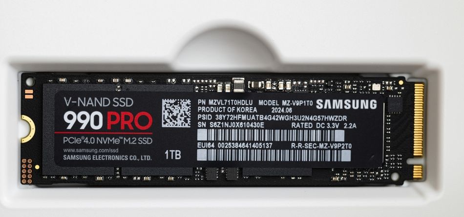
NVMe Solid State Drives (SSDs): Unleashing Storage Performance
Non-Volatile Memory Express (NVMe) SSDs, especially those in the M.2 form factor, have been a major beneficiary of PCIe bandwidth increases. These drives typically utilize x4 PCIe lanes.
PCIe 3.0 x4 SSDs offered sequential read/write speeds generally capping around 3,500 MB/s.
PCIe 4.0 x4 SSDs roughly doubled this, with many drives achieving sequential speeds in the range of 7,000 to 7,400 MB/s.
PCIe 5.0 x4 SSDs represent another significant leap. Theoretically, an x4 PCIe 5.0 link can provide approximately 16 GB/s of unidirectional throughput. Commercially available PCIe 5.0
SSDs are now reaching sequential read speeds exceeding 14,000 MB/s, with write speeds also being substantially higher than their PCIe 4.0 counterparts.
This massive increase in storage throughput directly benefits workloads involving large file transfers, professional 4K and 8K video editing, AI model training where large datasets are frequently accessed, and game loading times, especially with the adoption of technologies like Microsoft's DirectStorage API.
Network Interface Cards (NICs) and Other High-Bandwidth Peripherals
Beyond GPUs and SSDs, other peripherals greatly benefit from the bandwidth offered by PCIe 5.0. High-speed Network Interface Cards, such as those supporting 200 Gigabit Ethernet (200GbE) or 400 Gigabit Ethernet (400GE) and beyond, require substantial I/O throughput. A PCIe 5.0 x8 slot can provide approximately 64 GB/s of bidirectional bandwidth, while an x16 slot offers around 128 GB/s.
Similarly, AI accelerators, Field-Programmable Gate Arrays (FPGAs), and other specialized processing cards used in HPC environments and data centers can leverage the increased bandwidth of PCIe 5.0 for rapid data ingestion, inter-device communication, and offloading results.
Dominant Use Cases: Where Each Generation Excels
The suitability of PCIe 4.0 versus PCIe 5.0 often depends on the specific application and performance requirements.
PCIe 4.0: This generation remains highly relevant and offers a strong balance of performance and cost-effectiveness for a wide range of applications. It provides ample bandwidth for current-generation gaming GPUs, fast NVMe SSDs for mainstream and enthusiast PCs, and many server workloads.
PCIe 5.0: This generation is targeted at cutting-edge applications and systems that demand maximum I/O throughput and are designed to handle the most data-intensive tasks. Key areas include:
High-Performance Computing (HPC) and AI/ML Workloads: Essential for transferring massive datasets to and from accelerators (GPUs, FPGAs, custom ASICs) and for high-speed interconnect fabrics.
Data Centers and Enterprise Systems: Crucial for supporting next-generation networking infrastructure (400GbE and faster) and for powering ultra-fast storage arrays and hyperconverged infrastructure.
Enthusiast Gaming and Professional Workstations: Appealing to users who demand the absolute fastest storage solutions available and wish to future-proof their systems for upcoming generations of GPUs and other high-bandwidth peripherals, although the immediate benefits might be more application-specific rather than universal.
Suggested Reading: Putting high-performance computing into cars: automotive discrete semiconductors for autonomous driving
Design and Implementation Considerations for Engineers
Successfully designing and implementing systems with PCIe 4.0, and particularly the more demanding PCIe 5.0, requires careful attention to several critical engineering aspects.
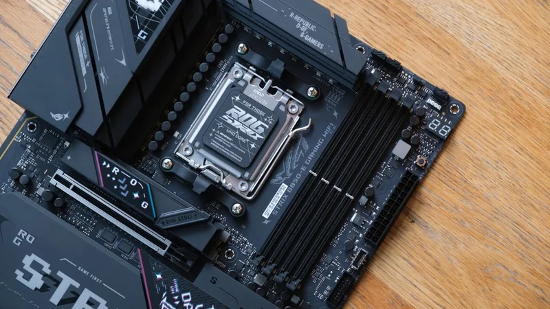
PCIe 5.0 PCB Layout and High-Speed Design Guidelines
The significantly higher data rates of PCIe 5.0 (32 GT/s per lane) make Printed Circuit Board (PCB) layout an extremely critical factor for maintaining signal integrity. Key considerations for high-speed design with PCIe 5.0 include:
PCB Material Selection: The choice of dielectric material is crucial. Standard FR-4 material, while common and cost-effective, exhibits significantly higher signal loss at the 16 GHz Nyquist frequency of PCIe 5.0 NRZ signals, especially over longer trace lengths. Low-loss or ultra-low-loss dielectric materials are often necessary to meet the -36dB channel insertion loss budget.
Controlled Impedance: Differential pairs must be routed with tightly controlled impedance, typically targeting 85 Ω or 90-100 Ω, depending on the specific implementation and specification details.
Trace Length Minimization and Matching: Traces should be kept as short as possible to reduce overall signal attenuation. Within each differential pair, the lengths of the two traces must be precisely matched to prevent intra-pair skew, which can degrade the differential signal.
Via Design: Vias allow signals to transition between PCB layers. They are significant sources of impedance discontinuity and signal reflection at high frequencies. Careful design, including optimizing via stub lengths or using micro-vias, is essential.
Minimizing Layer Transitions: Each layer transition via introduces some signal degradation. Therefore, routing high-speed PCIe signals with a minimum number of layer changes is preferred.
Suggested Reading: What is a Multilayer PCB?
The Path Forward: Beyond PCIe 5.0
PCIe continues to evolve beyond Gen 5 to meet escalating bandwidth demands, with PCIe 6.0 already released. Understanding this progression contextualizes the PCIe 4.0 to 5.0 transition.
A Glimpse into PCIe 6.0
PCIe 6.0 doubles the raw data rate again to 64 GT/s per lane, offering 256 GB/s bidirectional bandwidth on an x16 link. This leap required fundamental changes:
PAM4 (Pulse Amplitude Modulation with 4 levels): Transmits 2 bits per unit interval, maintaining PCIe 5.0's 16 GHz Nyquist frequency despite doubling the data rate, which helps manage channel loss.
FLIT (Flow Control Unit) Mode Encoding: Replaces 128b/130b encoding for higher efficiency.
FEC (Forward Error Correction): A lightweight mechanism to correct errors, crucial for PAM4's higher raw Bit Error Rate.
L0p (Low Power State): A new active power-saving state that allows reduced bandwidth and power consumption.
These changes represent a more significant architectural shift than the primarily physical layer focus of PCIe 4.0 to 5.0.
Conclusion
The jump from PCIe 4.0 to PCIe 5.0 significantly boosts high-speed interconnects, driven by demanding data-intensive applications. PCIe 5.0 doubles the raw data rate to 32 GT/s per lane, achieving nearly 128 GB/s bidirectional bandwidth on an x16 link. This leap was largely due to major physical layer advancements, tackling signal integrity challenges at 16 GHz NRZ signaling. These include advanced equalization, mandatory transmitter precoding, a tighter -36dB channel loss budget, and stricter clock jitter specifications. While PCIe 4.0 introduced features like extended tags for efficiency at 16 GT/s, PCIe 5.0 builds on these, focusing its innovation on electrical and signaling improvements.
Choosing between PCIe 4.0 and 5.0 depends on application needs, budget, and future-proofing. PCIe 5.0 excels in bandwidth-hungry applications like next-gen NVMe SSDs, 200/400GE networking, and AI/ML accelerators. However, for many current systems, including gaming PCs where GPUs don't saturate PCIe 4.0, it remains a cost-effective choice. Engineers adopting PCIe 5.0 must meticulously address PCB layout, thermal management, and complex signal integrity solutions, often requiring retimers.
FAQ Section
1. What is the main advantage of PCIe 5.0 over PCIe 4.0?
PCIe 5.0 doubles the raw data transfer rate to 32 GT/s per lane from PCIe 4.0's 16 GT/s. This results in a doubling of theoretical bandwidth (e.g., ~128 GB/s vs. ~64 GB/s for an x16 bidirectional link), enabling significantly faster data movement for demanding peripherals like high-speed SSDs and network cards.
2. Is PCIe 5.0 backward compatible with PCIe 4.0 devices and slots?
Yes, PCIe 5.0 maintains full backward compatibility with PCIe 4.0, 3.x, 2.x, and 1.x. A PCIe 5.0 device can operate in a PCIe 4.0 slot, and a PCIe 4.0 device can operate in a PCIe 5.0 slot. The link will negotiate to the highest common speed supported by both components.
3. What are the key physical layer changes in PCIe 5.0 that enable 32 GT/s?
Key changes include a more stringent channel loss budget (-36dB at 16 GHz), enhanced equalization techniques (e.g., 3-tap DFE, 2nd-order CTLE), mandatory transmitter precoding when requested by the receiver, tighter reference clock jitter specifications (e.g., 0.15ps RMS target), and electrical/mechanical improvements to connectors to enhance signal integrity at the higher 16 GHz NRZ signaling frequency.
4. Do current GPUs fully saturate PCIe 4.0 bandwidth, and what does PCIe 5.0 offer them?
Most current high-end gaming GPUs (e.g., NVIDIA RTX 40-series, AMD Radeon RX 7000-series) do not fully saturate PCIe 4.0 x16 bandwidth in typical gaming scenarios; the performance difference compared to PCIe 3.0 x16 is often minimal. PCIe 5.0 primarily offers future-proofing for next-generation GPUs that might handle larger datasets for AI tasks, require faster VRAM access for higher resolutions and textures, or engage in more complex compute workloads. Immediate gaming benefits from a PCIe 5.0 interface for current GPUs are generally modest.
5. What is precoding in PCIe 5.0, and why is it important?
Precoding is a signal processing technique that is mandatory for PCIe 5.0 transmitters operating at 32 GT/s if the receiver requests it during link training. It is important because it helps to mitigate the impact of burst errors, which can be introduced by Decision Feedback Equalizers (DFEs) in the receiver, a common equalization component at high speeds. Precoding transforms a potential burst error into two distinct, typically smaller, errors (an entry error and an exit error), making them potentially easier for the link's overall error detection and correction mechanisms to handle, thereby improving link reliability at the demanding speeds of PCIe 5.0.21
References
- https://www.design-reuse.com/news/245-pci-sig-publishes-pci-express-4-0-revision-0-9-specification/
- https://www.onlogic.com/blog/pcie-5-0/
- https://www.tomshardware.com/news/what-we-know-about-pcie4,39063.html
- https://www.keysight.com/blogs/en/inds/2020/03/30/pcie-standards-what-you-need-to-know
- https://www.keysight.com/us/en/assets/7018-06248/white-papers/5992-3141.pdf
- https://www.synopsys.com/glossary/what-is-pci-express.html
- https://www.amphenol-cs.com/connectors/pcie-connectors.html
- https://www.trentonsystems.com/en-gb/blog/pcie-gen4-vs-gen3-slots-speeds
- https://blog.acer.com/en/discussion/2509/pcie-gen-4-0-vs-5-0-is-the-upgrade-worth-it-for-the-latest-50-series-graphics-cards
- https://www.fs.com/blog/pcie-50-vs-pcie-40-which-one-to-choose-4032.html
- https://www.elepcb.com/blog/pci-and-pcie-in-pcb-layout-design/
- https://www.jays.co.kr/12_Files/Evolution-of-PCIe-Standards-and-Test-Requirements.pdf
- https://www.trsrentelco.com/sites/default/files/resources-pdfs/The_Evolution_of_PCIe_Standards_and_Test_Requirements.pdf
- https://www.tek.com/en/blog/pcie-making-science-fiction-capabilities-reality
- https://www.viavisolutions.com/en-us/products/pcie-40
- https://pcisig.com/doubling-bandwidth-under-two-years-pci-express%C2%AE-base-specification-revision-50-version-09-now
- https://www.techradar.com/computing/computing-components/what-is-pcie-5-0
- https://www.trsrentelco.com/sites/default/files/resources-pdfs/The_Fast_Track_to_PCIe_5_0_Doubling_the_Throughput_of_PCIe_4_0_to_32_GT_s.pdf
- https://pcisig.com/blog/doubling-bandwidth-under-two-years-pci-express%C2%AE-base-specification-revision-50-version-09-now-0
- https://www.rambus.com/blogs/pci-express-5-vs-4/
- https://www.keysight.com/blogs/en/tech/educ/pcie-5
- https://www.aewin.com/application/pcie-5-0-harnessing-the-power-of-high-speed-data-transfers/
- https://semiengineering.com/delivering-breakthrough-performance-and-power-efficiency-with-pcie-6/
- https://pcisig.com/pci-express-6.0-specification
- https://blog.samtec.com/post/why-did-pcie-6-0-adopt-pam4-there-are-many-reasons/
- https://www.graniteriverlabs.com/en-us/technical-blog/pcie-dynamic-link-equalization
- https://www.analogbits.com/wp-content/uploads/2020/08/CLN5-PCIe4-Ethernet-SERDES-PHY-Product-Brief.pdf
- https://www.asteralabs.com/pci-express-retimers-vs-redrivers-an-eye-popping-difference/
- https://www.asteralabs.com/resources/faqs/
- https://scolton.blogspot.com/2024/01/pcie-deep-dive-part-4-ltssm.html
- https://www.asteralabs.com/pcie-retimers-vs-redrivers-ensuring-signal-integrity-for-ai-infrastructure/
- https://c-payne.com/products/mcio-pcie-gen5-host-adapter-x16-retimer
- https://www.rambus.com/interface-ip/pci-express-glossary/
- https://www.ssstc.com/knowledge-detail/difference-pcie-gen4-gen5-enterprise-ssd/
- https://www.kingston.com/en/blog/pc-performance/pcie-nvme-ssd-gen3-gen4-gen5-video
- https://www.corsair.com/us/en/explorer/diy-builder/storage/gen-4-vs-gen-5-m2-ssds/
- https://www.tomshardware.com/reviews/best-ssds,3891.html
- https://www.reddit.com/r/nvidia/comments/1iad6mc/pcie_50_vs_40_vs_30_on_the_rtx_5090/
- https://gamersnexus.net/gpus/nvidia-rtx-5090-pcie-50-vs-40-vs-30-x16-scaling-benchmarks
- https://www.reddit.com/r/nvidia/comments/1iby6ip/nvidia_rtx_5090_pcie_50_vs_40_vs_30_x16_scaling/
in this article
1. Key Takeaways:PCIe 5.0 vs 4.0: Understanding the Generational Leap in High-Speed Interconnects3. What is PCIe?PCIe 5.0 vs 4.0 - Core SpecificationsArchitectural Evolution: A Layer-by-Layer Analysis of PCIe 5.0 vs 4.0Performance, Power, and Practicality: PCIe 5.0 vs 4.07. The Ecosystem: Hardware Support and Real-World Applications8. Design and Implementation Considerations for EngineersThe Path Forward: Beyond PCIe 5.010. Conclusion11. FAQ Section12. References