Understanding RF Circuit Fabrication and Interconnects
Article #4 of Mastering RF Engineering: High-frequency performance in RF systems depends on more than just components, it begins with the circuit itself. Advances in materials, fabrication, and interconnect design are redefining how modern RF systems achieve unmatched performance and reliability.

23 Dec, 2025. 14 minutes read
This is the fourth article in our multi-part series on “Mastering RF Engineering,” brought to you by Mouser Electronics. The series explores how RF technology is designed, built, and tested, highlighting the principles, components, and applications that make modern wireless systems possible. Each installment introduces a new dimension of RF engineering, giving readers a structured path from fundamentals to advanced practice.

Articles from this series:
- An Introduction to RF Theory, Practices, and Components
- Understanding RF Signal Chains: Key Building Blocks and Components
- How to Specify an RF Antenna: RF Antenna Operation, Design, Selection, Testing, & Verification
- Understanding RF Circuit Fabrication and Interconnects
- Digital RF Technology Explained: How Digital Signal Processing is Revolutionizing Wireless Systems
- Understanding RF Applications: Communication, Sensing, Power Transfer and Beyond
- The Fundamentals of RF Testing and Measurement Techniques
Modern radiofrequency (RF) systems depend on precise circuit fabrication and interconnect technologies to provide reliable, high-frequency performance. From wireless communication to radar to advanced sensing applications, RF circuits must be carefully designed to handle signal integrity, minimize loss, and meet demanding performance requirements.
RF components and devices are manufactured, assembled, and connected (electrically and physically) in various ways to meet diverse end-user requirements. The basic RF circuits within many RF system modules are RF circuit boards or planar circuits fabricated using planar circuit technologies. These RF circuits are then connected to other circuits using RF interconnects, such as waveguides, coaxial connectors, or wire bonds. RF circuits can be connected within the same housing, between housings, or even between systems using RF interconnects.
This article presents an overview of various RF circuit fabrication technologies and the most common types of RF interconnects, with an emphasis on coaxial cables and connectors. It details the key technologies, material considerations, and performance trade-offs engineers should understand when developing RF systems.
RF Circuit Fabrication Technologies
Three primary materials are used to make nearly all RF circuits: conductors, dielectrics, and semiconductors. For ease of machining, process control, and other factors, most RF circuits are developed using planar circuit technologies, employing methods such as printed circuit boards (PCBs), flexible PCBs, high-temperature co-fired ceramics (HTCCs), low-temperature co-fired ceramics (LTCCs), and integrated circuits (ICs).
More recently, some RF circuits and components are being made with 3D technologies and other specialized fabrication approaches that can be considered 2.5D. 3D circuits allow complete vertical integration, whereas 2.5D circuits refer to structures that stack multiple layers but don't fully integrate components in all three dimensions.
For most RF circuits, PCB, HTCC/LTCC, and IC technologies are dominant. These circuit technologies require developing an RF circuit using conductors, dielectrics, and semiconductor structures over a single 2D layer that is then bonded to or used as a platform to create additional layers. Interlayer interconnects, sometimes called vias, are often used to connect circuits between layers. Vias are small conductive pathways that electrically connect different PCB layers, allowing for compact, multilayer designs with improved signal routing. This layering technique allows for increased circuit density and improved RF performance, making it a critical factor in modern high-frequency designs. Interconnecting layers in RF and high-speed digital circuits is a complex task, using advanced methods and spurring ongoing research that explores new solutions.
PCBs & Flexible Circuits
PCB technology is based on the use of relatively thin dielectric substrate layers, called laminates, which are commonly made from glass fabrics and other composites bound with resins and flattened into sheets. PCB laminates may also be made of composite materials that include polymers or polymer foams for enhanced RF performance. Thin metallic foils, typically electroplated or rolled annealed copper, are laminated to the top and bottom surfaces and patterned to provide interconnection between components placed on or through the PCB materials. These metallic layers can also be used to form some passive RF circuits, such as power dividers and combiners, couplers, filter elements, planar transmission lines, and planar waveguides.
The most common method of patterning the metallic foils for PCBs is etching. While alternative methods to etching, such as laser ablation and milling, exist, they are typically limited to small custom batches or prototypes and are not commonly used in the mass production of PCBs. In large-scale manufacturing, PCBs are often plated with metals like nickel, tin, silver, palladium, and gold. These metal platings enhance conductivity, improve corrosion resistance, and aid in the solderability of surface metal contacts, pads, and vias.
Multiple layers of laminates and metallic foils can be used to fabricate extremely complex circuits with metallized vias that allow for interconnection between the layers. These multilayer designs are essential for reducing signal loss and improving impedance matching in high-frequency RF applications. Designers can make 2.5D structures using carefully constructed layers of laminates, foils, and metalized vias, such as strip line transmission lines, filters, waveguides, and other passive components.
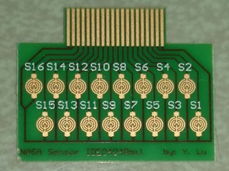
Typically, the external components and devices integrated into a PCB are either surface mount technology (SMT) parts placed on the top and bottom (Figure 1) or through-hole components connected to vias that penetrate the entire PCB stack and protrude from the top or bottom of the PCB. Sheet capacitive and resistive films can be integrated into the PCB stack and used to develop resistors and capacitors within internal PCB layers. Moreover, there are methods of spiraling or patterning metallic layers to make inductors, transformers, magnetic field sensors, and even motors.
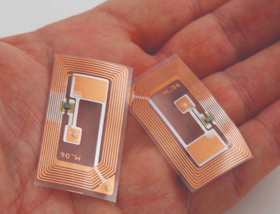
A flex circuit (Figure 2), or flex PCB, is a PCB technology that uses extremely thin laminate layers or intrinsically flexible materials to develop a circuit that is lighter, conforms to non-planar geometries for mounting, and can be used as a sticker, integrated into clothing, or for other purposes.
Due to the need to etch or machine the metallic foils, there are practical limits to the dimensions and proximity of PCB conductive elements. Depending on the machine or etching method, these tolerance limitations constrain how narrow the conductive traces and elements can be and how tightly they can be spaced. These constraints impact the size of planar transmission lines, coupled structures, filters, waveguides, and other high-frequency RF elements, ultimately limiting PCB technology's upper-frequency capability.
HTCC & LTCC
HTCC and LTCC planar technology differs from PCB technology in a variety of ways. These ceramic circuit technologies are advantageous in high-frequency, high-power, and harsh-environment applications due to their excellent thermal stability, low signal loss, and ability to withstand extreme temperatures and mechanical stress. Unlike PCBs, which rely on organic materials that can degrade over time, ceramic-based circuits offer superior reliability and durability in aerospace, defense, and industrial applications.
These technologies are based on using planned layers of ceramic, often alumina (aluminum oxide, Al2O3) or beryllium oxide (BeO), with conductive, resistive, or dielectric elements screen-printed or photo-imaged as pastes on the ceramic substrate sheet or tape. These layers of ceramic substrates or tapes, pastes, and any embedded components are then fired (known as sintering) in a stack to create a final circuit. LTCC is generally sintered at less than 1000°C, while HTCC may be sintered as high as 1600°C. Due to the sintering temperatures and metallic compatibility, LTCC technologies can use low-resistivity conductors, like silver and gold, while HTCC processes (Figure 3) tend to rely on molybdenum and tungsten due to the refractory temperatures. A key advantage of LTCC technology is its ability to integrate passive components such as resistors, capacitors, and inductors directly into the ceramic layers, reducing circuit size and improving performance by minimizing parasitic elements and signal interference.

HTCC and LTCC technologies tend to survive very high temperatures, have a low coefficient of thermal expansion (CTE) compared to PCBs, and can be hermetically sealed as part of the fabrication process.
IC Technology
IC microelectronic technology is the foundation for many active devices and some passive RF components. There are several names for different classes of IC used in RF technology, including RFIC and microwave monolithic IC (MMIC). Many past RFIC and MMIC designs resulted in a chip with a single function, such as a power amplifier, low-noise amplifier (LNA), mixer, or switch, made with processes or semiconductor materials that exhibit better RF characteristics. RFICs are typically mounted on other RF circuit technologies to realize parts and systems.
Unlike traditional RF ICs that focus on a single function, RF systems-on-chips (RFSoCs) and RF systems-in-packages (RFSiPs) integrate multiple RF components, such as amplifiers, mixers, and converters, into a single package, enabling highly compact and programmable RF systems.
ICs are manufactured in semiconductor fabrication facilities that require substantial infrastructure and equipment. RF circuit design and implementation using this technology is highly complex, requiring intricate supply chains and specialized expertise. Hence, there are dedicated chip manufacturers and fabless design houses that partner with chip fabricators to produce RFICs that supply most of the commercially available RF chips. Some governments and private organizations own chip fabrication facilities and leverage these to be more competitive and to develop protected technologies.
Specialized & Custom Processes
There are several specialized and custom processes for manufacturing RF circuits, including laser-defined structuring (LDS) and micro-coaxial technology. LDS processes use a laser to catalyze metallic particles within a carrier material, allowing conductor deposition or plating. This technology is often used in very dense electronics housing for antennas, such as smartphones and tablets. Micro-coaxial technology uses proprietary methods to develop 3D metallic structures that can be used to build true coaxial transmission lines or waveguides as interconnects for embedded components in a high-precision platform. There is continual development in 3D printing technologies, such as fused-deposition modeling (FDM), laser sintering, and digital-light processing (DLP), to build RF circuit technologies. Examples include multi-filament printing FDM with dielectrics and conductors to make RF components, plating DLP-based parts, and directly printing metallic structures with laser metal sintering.
RF Interconnect Technologies
For RF circuits to function, electromagnetic energy in the RF spectrum that is either generated by or captured by a transducer must somehow reach the circuit components. Because free-space propagation results in signal characteristics that are not ideal for most RF circuits, designers generally use interconnect methods that efficiently capture and direct electromagnetic energy.
Often, circuit designs use conductors or dielectrics as interconnects to form transmission lines or waveguides. However, many RF modules and systems require external RF circuit connections to the antenna, other modules, or other RF systems. For example, in test and measurement or automated manufacturing applications, interconnects such as spring pins (pogo pins) or probes allow for repeated cycling at relatively rapid speeds. There are also more permanent interconnecting methods, such as wire bonding, for binding IC contacts to packages or between ICs.
Waveguides
Waveguides are hollow conductive structures that "guide" electromagnetic energy within a specific maximum and minimum (i.e., banded) frequency along the structure.
Unlike coaxial cables, which can carry signals down to DC (0Hz), waveguides function efficiently only above a specific frequency, known as the cutoff frequency. Below this threshold, electromagnetic waves cannot propagate, leading to signal attenuation instead of transmission. The cutoff frequency is determined by the waveguide's physical dimensions, which are proportional to the wavelength of the signals they carry. This means that lower-frequency waveguides must be physically larger, while higher-frequency waveguides can be much smaller.
Waveguides are highly efficient at guiding electromagnetic energy with minimal loss, making them ideal for high-frequency, high-power, and sensitive RF applications. They are also physically rugged, which contributes to their widespread use in aerospace, defense, and industrial settings. Waveguide components, such as filters, power dividers and combiners, attenuators, and antennas, can be constructed with relatively simple metallic structures but may also incorporate complex designs to expand bandwidth or enhance performance. Since waveguides and coaxial technologies are often used together in RF systems, various adapters and transition components exist to facilitate seamless interconnection.
Twisted Pair, Twinaxial, & Triaxial
Twisted pair, twinaxial, and triaxial interconnects are all forms of transmission lines. Twisted pair systems, such as those used with old telephony wiring and Ethernet category cabling, are made using a pair of insulated conductors wrapped around each other to form a crude transmission line. This method does not provide any shielding but is more efficient for signal transfer at lower frequencies than a single conductor or radiation.
Twinaxial and triaxial are like coaxial interconnects, but twinaxial transmission lines have an additional center conductor (forming a twisted-pair balanced line), and triaxial transmission lines have an additional outer conductor. Twinaxial is predominantly used for short-range and high-speed differential signaling to tens of megahertz (generally less than 200MHz). Triaxial cables can be driven so that the internal shielding is floating, which provides enhanced shielding and protection from outside noise. Triaxial cables are used for high-frequency transducers, precision measurement equipment, and applications requiring low-impedance transmission lines.
Wire Bonds & Probes
Wire bonding is a method of permanently attaching bond pads on ICs to package leads or PCB traces using fine wires. Wire bonding is mostly used to connect chips with packaging or bare die to an RF circuit board. This interconnect technology requires specialized wire bonding machines to properly and reliably connect wire bonds, which is why wire bonding in large volumes is typically done using automation.
Probes allow temporary or repeated connections in RF circuits and are commonly used in automated testing, diagnostics, and high-frequency measurement setups. A wide variety of probe technologies exists, including spring probes, spring pins, and transmission line arrangements that use multiple probes in a probe head. Contactless probe designs also use near-field antennas, open-ended coaxial lines, and even waveguides.
Coaxial
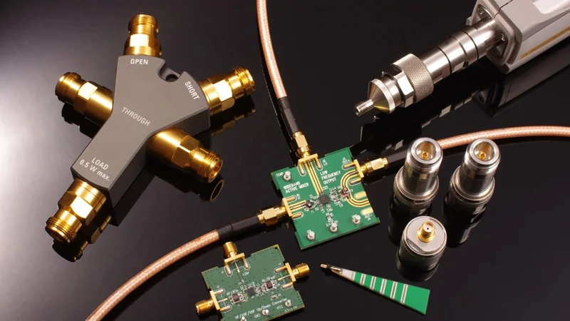
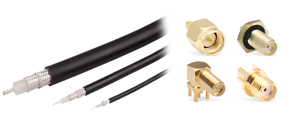
Coaxial transmission lines are one of the most common types of RF interconnects used beyond the chip and circuit board level. These transmission lines are used for board-to-board connections, within modules, between modules, and between systems. A benefit of coaxial transmission lines is that the outer conductor also acts as a shield that prevents internal signal leakage and external signal ingress into the transmission line environment. These properties and the relatively efficient transmission of signal energy along a coaxial line have led to the widespread use of coax in RF, high-speed digital signaling, precision measurement, and many other applications.
The main physical components of a coaxial transmission line are a coaxial cable and connectors. However, there are some applications where the coaxial cable is directly attached to other transmission lines, or a coaxial connector may be the interface to another transmission line, such as with end-launch coaxial connectors (Figure 4).
Coaxial transmission lines are characterized by cylindrical, coaxial inner and outer conductors that are separated by a dielectric barrier (Figure 5). Within a coaxial transmission line, the magnetic field lines follow a circular path around the inner conductor and between the inner and outer conductors. The electric field lines are perpendicular to the magnetic field lines and radiate from the inner conductor to the outer conductor.
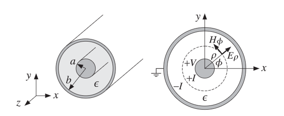
This transverse electromagnetic (TEM) mode of operation leads the Poynting vector to point along the length of the coaxial transmission line. This behavior results in relatively simple derivations of the ideal characteristic impedance, inductance per unit length, capacitance per unit length, voltage, current, and other transmission line behavior.
In the following equation, Z is the characteristic impedance, η is the wave impedance, μ is the magnetic permeability, ε is the relative permittivity of the dielectric, L' is the inductance per unit length, and C' is the capacitance per unit length.

In an ideal coaxial cable, the electromagnetic fields propagate in TEM mode, meaning electric and magnetic fields are perpendicular to each other and the direction of travel. However, at higher frequencies, additional modes (like TE11) start to appear, impacting signal integrity.
It is also possible to estimate the loss per unit length of a coaxial transmission line using the ohmic and dielectric losses of the conductors and dielectrics used in the coaxial line construction. The following equation, where 𝛂 is the attenuation per unit length, 𝛂c is the ohmic losses of the conductors, 𝛂d is the dielectric losses, Rs is the resistivity of the conductors, and tan𝛿 is the loss tangent of the dielectric, shows that the attenuation of a coaxial line is greater for smaller dimensions of a and b.

Coaxial cables are broadband interconnects, which can operate down to DC (0Hz). However, their upper cutoff frequency is determined by their physical geometry, as higher frequencies can introduce additional propagation modes beyond the fundamental TEM mode. Specifically for coax, the TE11 mode begins to propagate above a certain cutoff frequency and is approximated by the following equation, where fc is the cutoff frequency, c is the speed of light, λc is the cutoff wavelength, 𝑎 and b are dimensions of the transmission line, μ𝑟 is the relative permeability, and εr is the relative permittivity:

If modes other than TEM are operating within the transmission lines, the reflections of the higher-order modes can cause interference, increase loss, and reduce the transmission line’s voltage standing wave ratio (VSWR) performance. Larger coaxial cables have a lower cutoff frequency but can handle higher voltages and power while exhibiting lower attenuation per unit length compared to smaller coaxial cables.
There are three main types of available coaxial cable: rigid, semi-rigid, and flexible. Rigid coaxial cable must be manufactured to exact specifications and tends to be the highest-performing coaxial cable. Semi-rigid coaxial cable can be formed to shape using appropriate tools (or by hand in some cases), but then it can no longer be bent without risking damage. Flexible coaxial cable sacrifices attenuation and shielding effectiveness to allow for flexibility. Moreover, flexible coaxial cables typically require a jacket to ensure that they maintain coaxiality and are protected from physical abrasion and other physical stresses. A wide variety of specialized constructions for flexible coaxial cables ensures that they offer phase stability, amplitude stability, and consistent behavior over a wide range of environmental factors.
RF Circuit Design Solutions by Analog Devices and Mouser Electronics
With products engineered for wideband operation and low signal loss, Analog Devices and Mouser Electronics provide the tools that drive next-generation RF design and testing.
Analog Devices Inc. ADL8103-EVALZ Evaluation Board
The Analog Devices ADL8103-EVALZ Evaluation Board provides a complete and easy-to-use platform for evaluating the ADL8103 broadband LNA, which operates from 6GHz to 12GHz. Built on a 2-layer high-frequency PCB, the board is engineered for low loss and consistent impedance across its RF paths. With 50Ω input and output traces, end-launch SMA connectors, and a through calibration path, it enables precise performance testing and repeatable measurements for engineers working on high-frequency front-end circuits. Its design emphasizes signal integrity and minimizes parasitic effects that can distort measurements in wideband RF environments.

Supporting flexible biasing and power-supply configurations, the ADL8103-EVALZ facilitates performance characterization across different operating conditions, making it ideal for lab evaluation and design validation. The board’s compact footprint and robust material stack, featuring Rogers 4350B and Isola 370HR laminates, ensure low dielectric loss, making it suitable for applications requiring consistent gain and low noise over broad frequency ranges. It serves as a versatile reference for integrating the ADL8103 into test instrumentation, radar, or communication systems, where linearity and low noise are critical.
Analog Devices Inc. ADL8113 LNA
The Analog Devices ADL8113 LNA delivers wideband amplification and high linearity performance across 10MHz to 12GHz, making it an excellent choice for broadband receivers and measurement systems. Its integrated bypass switches provide four selectable modes, two internal and two external, allowing designers to optimize system gain and noise performance dynamically. With a 14.0dB typical small-signal gain and 3.8dB noise figure, the ADL8113 maintains consistent performance across frequency, temperature, and supply variations, ensuring stable operation in diverse RF environments.

Designed for easy integration into modern RF front ends, the ADL8113 features a land grid array (LGA) package (6mm × 6mm, 28-terminal) and internal power-supply decoupling, minimizing external component count and board space. Its combination of high gain, linearity, and configurable bypass paths allows engineers to simplify complex receiver chains while maintaining superior dynamic range. The device’s rugged temperature range of -40°C to +85°C and RoHS compliance further position it as a reliable building block for test and measurement systems, electronic warfare, and next-generation wireless receivers.
Conclusion
RF circuits and interconnects are critical technologies for nearly all modern electric and electronic devices. Virtually all modern technological applications use some form of RF wireless communication, sensing, power transfer, or directed energy, and this will likely only increase as more technologies are electrified and controlled via advanced electronics.
As RF applications continue to evolve with 5G, 6G, satellite-based connectivity, and artificial intelligence (AI)-powered wireless systems, innovations in miniaturization, advanced materials, and 3D fabrication techniques will expand RF circuit design. Understanding the strengths and trade-offs of PCB, HTCC, LTCC, and IC technologies and various RF interconnects helps make informed design decisions to improve signal integrity, reduce losses, and set the stage for next-generation RF solutions.
References
[1] Pierce M. Sensing Opportunities: NASA-Developed Sensor Technologies Available for New Commercial Products. NASA Technology Transfer Program Blog. 2025 Jan 29. Available from: https://technology.nasa.gov/blog-sensing-opportunities
[2] Chen L-Y, Neudeck PG, Spry DJ, Beheim GM, Hunter GW. 500°C Electronic Packaging and Dielectric Materials for High Temperature Applications. NASA Glenn Research Center; 2017. Available from: https://ntrs.nasa.gov/api/citations/20170003040/downloads/20170003040.pdf
[3] Sophocles J. Orfanidis, Electromagnetic Waves and Antennas (Rutgers University, 2016), 546, fig. 11.4.1, https://rutgers.box.com/s/rwzifofsu9slf8xy38f6uwhjd5gmn2q7; accessed via https://www.ece.rutgers.edu/orfanidis.

This article was originally published by Mouser Electronics. It has been edited by the Wevolver team and Ravi Y Rao for publication on Wevolver. Upcoming articles in this series will continue to explore key areas of RF engineering, offering engineers practical insights into the design and implementation of modern RF systems.