The Fundamentals of RF Testing and Measurement Techniques
Article #7 of Mastering RF Engineering: RF testing and measurement are essential to achieving accuracy and reliability in wireless systems. They ensure that every component and signal path performs as intended across varying frequencies, environments, and applications.

30 Dec, 2025. 13 minutes read
This is the seventh and the final article in our multi-part series on “Mastering RF Engineering,” brought to you by Mouser Electronics. The series explores how RF technology is designed, built, and tested, highlighting the principles, components, and applications that make modern wireless systems possible. Each installment introduces a new dimension of RF engineering, giving readers a structured path from fundamentals to advanced practice.

Articles from this series:
- An Introduction to RF Theory, Practices, and Components
- Understanding RF Signal Chains: Key Building Blocks and Components
- How to Specify an RF Antenna: RF Antenna Operation, Design, Selection, Testing, & Verification
- Understanding RF Circuit Fabrication and Interconnects
- Digital RF Technology Explained: How Digital Signal Processing is Revolutionizing Wireless Systems
- Understanding RF Applications: Communication, Sensing, Power Transfer and Beyond
- The Fundamentals of RF Testing and Measurement Techniques
Given the precision required to design, fabricate, assemble, and deploy RF technology, it's not surprising that RF systems require significant test and measurement system infrastructure throughout the development and deployment processes. Beyond this, many RF systems must be maintained and adjusted throughout their lifespan, requiring additional test equipment and measurement techniques. Plus, organizations must adhere to spectrum regulations and meet minimum requirements set by RF standards and certification organizations.
This article explores how RF devices and systems are tested, covering measurement techniques, test types, equipment, accessories, and why testing is critical throughout RF system development.
Why Test RF Devices and Systems?
Engineers test and measure RF components, devices, assemblies, systems, and installations for various reasons. One of the most common is to ensure they meet local spectrum management regulations. Nearly every region around the globe has organizations that require technology with RF capabilities to meet particular frequency, power, electromagnetic compatibility (EMC), and safety regulations to be sold and operated legally within that region. These organizations often employ personnel and installations that use spectrum-monitoring equipment to capture signals transmitted within their region for inspection. Moreover, wireless communication standards bodies, such as the Wi-Fi Alliance, Bluetooth® Special Interest Group, and Connectivity Standards Alliance, require RF technologies to be tested and certified for their respective technologies.
Other types of testing include development and design verification (e.g., system prototyping and optimization, hardware modeling in software) and manufacturing and quality control (e.g., tuning, verification, maintenance).
RF testing and measurement are needed during RF hardware and software development. System developers often perform confirmation testing of new RF components or device specifications before selecting a component or device for a given design. RF component and device development usually involves an iterative process, with testing and measurement at each stage. This confirmation testing might include probing individual circuit elements on wafers or producing complete runs of chips or boards to evaluate new designs or modifications.
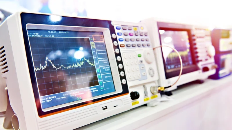
Engineers routinely test RF hardware during and after manufacturing to ensure that the parts operate to specifications. This can include benchtop testing as well as larger-scale evaluations (Figure 1). Some RF hardware designs include tunable or programmable features that allow engineers to adjust key hardware elements or software parameters that can modify the performance of the part to work within specifications. Examples include real-time testing of an RF filter while adjusting a resistor, capacitor, or inductor ratio of a resonator, or even adjusting tuning screws in a waveguide resonator.

When assembling an RF system, engineers often test sections as well as the entire system during and after assembly. This helps confirm that individual hardware elements are functioning properly when assembled, as troubleshooting the entire assembled system may present complexities that obfuscate defective parts, design errors, or assembly errors. When engineers install RF systems such as cellular or Wi-Fi services, they test them to ensure the installation meets contract specifications and regulatory requirements. They may also periodically test RF and wireless installations to confirm they operate within safety and regulatory parameters. These tests can include over-the-air tests, like spectrum monitoring, as well as testing via injecting signals and equipment to capture the signals within a system's conductive channels (e.g., during passive intermodulation (PIM) distortion testing).
Engineers often create RF hardware models using mathematics and physical testing results to simplify system design and minimize physical testing. For example, when designing a wireless device, engineers often develop the antenna and wireless system simultaneously. The prototype antennas can be physically tested to generate hardware models that are then used alongside the RF circuit hardware in simulations. With accurate and sophisticated models, simulations can reduce the scope of physical testing, particularly in early design and prototyping, which may drastically lower the development cost and time.
Some RF systems internally integrate RF testing to verify safety and performance. However, this is typically done with mission-critical equipment that incorporates dedicated internal testing circuits and hardware. With the rise of digital integration within RF systems, designers are increasingly able to integrate testing that can digitally synthesize and convert RF signals. Hence, it is possible to use coupled paths and switch matrices to test the signal response at key points in a signal chain as part of automated testing or tuning procedures on a circuit board, system-in-package (SiP), or system-on-chip (SoC).
How RF Measurements Are Made
The scope of RF measurement techniques and methods is incredibly expansive, and RF measurements can be made using different transmission mediums to convey and guide the test signal energy. In some cases, RF measurements are made in situ during the operation of the RF component, device, assembly, or system. In other cases, a single device under test (DUT) is isolated and tested in a configuration specifically designed for one or multiple RF measurements.
RF tests generally fall into two categories: those where test equipment generates signals to test the system, and those where it measures signals generated by the system under test (SUT). For instance, some RF testing can be done on wireless communication installations by remote equipment capturing ambient signals. In contrast, other testing would require sending test communication signals between a remote test unit or connecting directly to the wireless communication system and energizing RF circuits and interconnects to perform the measurements.
Precision RF measurements, which help reduce uncertainty within a measurement to capture meaningful physical insights about a test target, often include a calibration process to further minimize uncertainties associated with the test apparatus and ambient environmental factors. To help improve test system repeatability, regulatory and standards agencies release specifications for calibration standards, among other standards for test apparatuses. For example, such a standard may include specifications for the exact EMC environment within which a test must be conducted.
The two most relevant types of RF measurements are free-space testing, which refers to either radiated or near-field RF emissions, and conducted RF signal testing, which refers to RF emissions along a cable or power line (sometimes called "conducted" measurements). In free-space testing, antennas act as transducers that convert electrical signals into electromagnetic waves. Conducted testing uses components like calibrated loads, which are designed to absorb all signal energy and act as a precise reference for measurements.
Basics of RF Free Space
When conducted RF signals are transduced to radiated or coupled fields, the passing, reflected, absorbed, or coupled fields can be used to discern behaviors of RF materials and systems. Free-space measurements involve capturing the electromagnetic fields emitted by an RF system or exposing a DUT to externally generated fields. These tests are considered free space when there is no direct conductive contact and when the medium between the DUT and the test equipment is either air or a vacuum, rather than a physical transmission line or a non-air dielectric.
Some free-space testing, such as spectrum monitoring, uses equipment to capture ambient signal energy generated by natural and human-made signal sources. However, this free-space energy could also be intentionally focused to reflect or pass through a material (Figure 2), providing insights into the material's electromagnetic behavior, such as with microwave or millimeter-wave (mmWave) free-space dielectric characterization.

Some non-contact types of RF measurements, such as waveguide or open-ended transmission line probes, use the coupled fields generated by proximity to the exposed probe end and the DUT, material, or test system to determine the behavior of the test target.
In free-space testing, it's important to know which region of the field (near-field or far-field) the test apparatus is operating in and whether it's capturing or inducing signals. The way test apparatuses, such as test antennas and probes, interact with another system depends on the field dynamics, which could be in the reactive near-field, radiative near-field, far-field, or transition zones. Various models exist for processing information captured from test apparatuses in the different field zones. Each must be carefully applied to reduce errors, while several of these approximations are used only for specific applications or antenna types. The following equations show selected far-field region transition point approximations, where r is the distance to the far-field region, lambda (λ) is the radiation wavelength, D is the largest antenna dimension, and 𝑙 is the maximum antenna length:
Basics of RF Signal Measurements
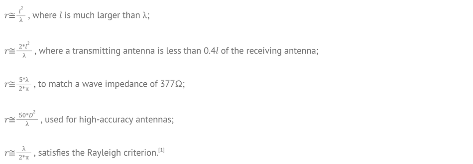
RF signals, or conducted measurements, use conductive pathways, mainly transmission lines and waveguides, to transmit or receive test signals (Figure 3). Using conductive measurement methods means that, ideally, all the signal energy is contained within the interconnect, test system, and DUT or SUT. Unlike free-space measurements, where only a fraction of the field energy is exchanged between the test system and test target, conducted measurements can more efficiently exchange energy between the test system and test target, as well as avoid external interference, depending on the loss of the interconnect and the quality of the shielding.
Most test equipment uses conductive pathways for some portions of the test apparatus, such as the interconnect and circuit paths from a probe to the transducer. If an RF system or DUT is designed with externally accessible test points, engineers can use conductive probes or an RF interface and interconnects with the exposed test points. This method is often used for quality control and verification testing or tuning RF circuits within a system that is inaccessible via external ports.
Basics of Antenna Testing
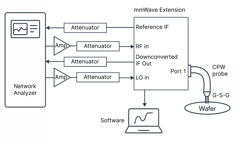
RF antennas often undergo rigorous testing, as these transducers are a key element in the behavior of RF systems that capture or radiate signals and are subject to regulatory and standards certification. Antenna testing involves transmitting or receiving signals between the antenna under test (AUT) and one or more reference antennas. In the simplest type of antenna testing, a single highly directional test antenna is placed in the desired field region of the AUT. Engineers often conduct this test in an open-air test range or in an RF shielding chamber to reduce external interference. More sophisticated antenna testing uses an array of antenna probes, often in the radiative near-field region, and a test apparatus that can distinguish the signals from each probe (Figure 4). The signal energy captured from the probes is then digitized and mathematically processed to extract the antenna behavior, including gain, directivity, efficiency, and antenna pattern.
There are also dedicated antenna test chamber designs with positioners that control a test antenna to capture the AUT's response at different azimuth and elevation positions. Anechoic-style chambers are often used for antenna testing to minimize internal reflections while providing a high level of RF shielding from external interference. Because an antenna's field region depends on the wavelength of the frequencies at which the antenna is tested, testing low-frequency antennas requires larger separation distances between the test antenna and the AUT, as well as between the antennas and the chamber walls, if a chamber is used. Antennas being tested over a wideband operation often need to be tested in larger chambers to accommodate the lowest frequency being tested.
RF Test Equipment
RF test equipment comprises hardware and software systems designed to generate, capture, and process the signals to and from RF SUTs. Common, general-purpose RF test equipment used throughout the industry includes network analyzers, spectrum analyzers, signal analyzers, power sensors, power meters, and signal generators. More specialized RF test equipment is also geared toward serving a given application. These are generally specialized variations of the general-purpose RF test equipment, including cable analyzers, antenna analyzers, and field test equipment.
Older test equipment used analog signal capture, signal generation, and measurement displays. Modern RF test equipment uses microprocessor units (MPUs), application-specific integrated circuits (ASICs), or fully functioning computer systems with advanced software capability. The past decade has seen a rise in modular test equipment that pairs a compact hardware test system with digital communication compatible with a PC and software for interfacing with the test unit. More complex test systems incorporate multiple modular, benchtop, or rack-mount RF test equipment in sophisticated automated systems with custom processing and control software for manufacturing or automated certification testing.
Power Sensors & Power Meters
Power sensors and power meters are relatively simple RF instruments that convert captured RF signal energy within the device's bandwidth into a power reading. Some RF power sensors use calibrated antennas to capture ambient signals, while others are connectorized instruments designed to test DUTs or calibrate test setups based on signal generators.
Network Analyzers and Vector Network Analyzers
A network analyzer is a tool designed to send a precisely controlled signal into an RF network while simultaneously capturing the reflections from the RF network. By comparing the timing and phase over frequency of the incident signal and reflected signal, engineers can determine the impedance, attenuation, and small signal gain, and derive network parameters, such as scattering parameters (S-parameters) and impedance parameters (Z-parameters).
A network analyzer that can determine the phase variations in the incident and reflected signals is called a vector network analyzer (VNA). A VNA with more than one port, known as a multiport VNA, can analyze the behavior of more complex multiport RF networks with fewer errors than the iterative approach necessary for single-port network analyzers. While single-, double-, and quad-port VNAs are the most common, some manufacturers offer up to 24 ports. Engineers can extend a VNA's port count using switch matrices or VNA port extenders, but these modular methods tend to result in reduced testing performance compared to true multiport VNAs. They may also require more complex calibration to reduce interconnect and environmental uncertainties.
Spectrum and Signal Analyzers
A spectrum analyzer captures the amplitude of RF signal energy over a range of frequencies. It does so instantaneously over a limited bandwidth or by using a frequency-sweeping method and converting that energy into a power reading plotted over the observed frequency range. A spectrum analyzer that measures a signal's amplitude and phase is called a vector signal analyzer (VSA), vector spectrum analyzer, or signal analyzer. This terminology distinguishes it from traditional spectrum analyzers, which measure only amplitude. With both amplitude and phase information of a captured signal, a signal analyzer can convert that information into the digital domain and process that signal for IQ data, which is useful in analyzing digital communication and sensing signals.
Signal Generator
A signal generator is designed to produce precise power and frequency RF signals. It is generally used to inject signal energy into the RF system under test. More sophisticated signal generators can include signal modulation and frequency sweeping and introduce other complex signal characteristics. The signals that a signal generator induces in a DUT are often captured by a spectrum analyzer, power meter, or multiple analyzers or meters if the DUT has multiple output ports.
Wireless Communications Test Systems
The rise of wireless communications has prompted the development of more complete wireless communications test equipment, compared to basic combinations of VNAs, signal analyzers, and signal generators with RF accessories. Several variations of these systems exist, but generally, they can generate and process wireless communication signals. These signals are used to interact with wireless communications hardware under test in such a way that allows for analysis of the behavior of the test system as part of a pre-certification, certification, software development, or prototyping process.
An example of this new type of RF test equipment is Keysight's series of Wireless Network Emulators, which test protocol, RF, functionality, and performance of wireless communication chips and devices. These systems are equipped with protocols and solutions for testing 5G, NR, RedCap, NTN, LTE, C-V2X, NB-IoT, Cat-M, Wi-Fi, W-CDMA, GSM, and other wireless communication standards.[3]
Integrating Advanced Wireless Interfaces into Modern RF Systems with STMicroelectronics and Mouser Electronics
From low-power Bluetooth® connectivity to high-frequency NFC sensing, modern RF platforms rely on specialized components that enable secure, efficient, and scalable communication. STMicroelectronics delivers these capabilities through advanced, low-power wireless solutions that strengthen connectivity, reliability, and system integration across diverse applications.
STMicroelectronics STM32WB09 Bluetooth® Low Energy 5.4 32-Bit MCUs
The STMicroelectronics STM32WB09 is a Bluetooth® Low Energy (BLE) 5.4-compliant wireless microcontroller designed for ultra-low-power operation and robust 2.4GHz RF performance. Built on an Arm® Cortex®-M0+ core with a dedicated BlueNRG coprocessor, it efficiently manages timing-critical BLE operations while maintaining excellent energy efficiency. The device supports Bluetooth Mesh networking and proprietary 2.4GHz protocols, making it ideal for applications requiring low latency, long range, and extended battery life.

Advanced hardware-based security features, including a true random number generator, AES-128 encryption, and public key acceleration, enhance data integrity and device protection. With integrated SMPS for power efficiency, multiple serial interfaces, and compact packaging options, the STM32WB09 delivers an optimal balance of performance, security, and energy savings for wireless systems.
Specification | Details |
Core Processor | Arm® Cortex®-M0+, up to 64MHz |
Radio Standard | Bluetooth Low Energy 5.4 and 2.4GHz proprietary |
RX Sensitivity | –97dBm @ 1Mbit/s, –104dBm @ 125Kbit/s |
TX Power | Up to +8dBm |
Memory | 512KB Flash, 64KB RAM |
Security | AES-128, TRNG, PKA, Secure Bootloader |
Power Modes | 12nA (Shutdown), 0.9µA (Deepstop) |
Voltage Range | 1.7V to 3.6V |
Operating Temp. | –40°C to +105°C |
Notable Interfaces | SPI, I²C, USART, LPUART, 12-bit ADC |
Package Options | VFQFPN32, WLCSP36 |
Applications | Industrial automation, asset tracking, smart lighting, healthcare, fitness, security, remote control, and a wide range of connected consumer and IoT applications |
STMicroelectronics X-NUCLEO-NFC10A1 NFC Card Reader Expansion Board
STMicroelectronics X-NUCLEO-NFC10A1 is an NFC card reader expansion board based on the ST25R200 device, designed to add HF RFID and NFC functionality to STM32 microcontroller platforms. It supports multiple standards, including ISO14443A/B and ISO15693, and can detect, read, and write NFC Forum Type 1, 2, 4, and 5 tags.

With its integrated 13.56MHz etched antenna, low-power wake-up system, and Arduino UNO R3 compatibility, the board simplifies development for applications like contactless payment, asset tracking, and industrial proximity sensing. Backed by STM32Cube-compatible firmware libraries, it enables quick evaluation and scalable NFC solutions for embedded systems.
Specification | Details |
Core IC | ST25R200 NFC reader |
Supported Protocols | ISO14443A/B, ISO15693 |
Operating Frequency | 13.56MHz |
Antenna | 47×34mm PCB-etched, 4 turns |
Supported Tags | NFC Forum Type 1, 2, 4, 5 |
Wake-Up Feature | Low-power tag detection and timed activation |
Interface | Arduino UNO R3 connector |
Software Support | STM32Cube firmware and examples |
Certifications | FCC, RoHS, WEEE |
Applications | NFC readers, RFID, access control, IoT interfaces |
Conclusion
RF test equipment encompasses various technologies and techniques for accurately and efficiently measuring the behavior of RF technologies. Beyond RF test equipment hardware, a wealth of measurement techniques, signal processing, software, and analysis tools enable users to interpret the results of the test information. As RF technology advances, RF test equipment and systems continue to exceed this pace to enable this advancement.
This concludes the Mastering RF Engineering series. Continue exploring the latest innovations, insights, and design resources at Mouser’s RF & Wireless Hub.
References
[1] COSMOS - The SAO Encyclopedia of Astronomy. Rayleigh Criterion [Internet]. Swinburne University of Technology. Available from: https://astronomy.swin.edu.au/cosmos/R/Rayleigh+Criterion
[2] Fung AK, Dawson D, Samoska L, Lee K, Oleson C, Boll G. On-Wafer Vector Network Analyzer Measurements in the 220–325 GHz Frequency Band [Internet]. Pasadena (CA): Jet Propulsion Laboratory, California Institute of Technology. Available from: https://dataverse.jpl.nasa.gov/api/access/datafile/12449?gbrecs=true
[3] Keysight Technologies. Wireless Network Emulators [Internet]. Santa Rosa (CA). Available from: https://www.keysight.com/us/en/products/wireless-network-emulators.html

This article was originally published by Mouser Electronics. It has been edited by the Wevolver team and Ravi Y Rao for publication on Wevolver. This series explored the key areas of RF engineering, offering engineers practical insights into the design and implementation of modern RF systems.