Operational Amplifier: Theory, Design and Applications for Engineers
An operational amplifier (op-amp) is a high-gain differential amplifier used in analog circuitry to process and condition signals. This article examines op-amp theory, ideal and real behavior, key specifications, core circuits, applications, and practical design considerations.

10 Feb, 2026. 13 minutes read
Key Takeaways
Operational amplifier fundamentals:
An operational amplifier (op-amp) is a high-gain differential amplifier that amplifies the voltage difference between its input terminals. When combined with external resistors and negative feedback, it enables precise amplification, filtering, integration, differentiation, and signal conditioning.Ideal vs. real op-amp behavior:
The ideal op amp assumes infinite open-loop gain, infinite input impedance, zero output impedance, and unlimited bandwidth. Real op amps exhibit finite gain, limited bandwidth, nonzero input offset voltage, input bias current, and constrained output swing, all of which directly affect circuit accuracy.Performance-limiting specifications:
Key parameters—including bandwidth, gain-bandwidth product, slew rate, common-mode rejection ratio (CMRR), power supply rejection ratio, and noise—define how an op-amp behaves in real circuitry and set practical limits on signal amplitude, frequency, and precision.Closed-loop operation and core circuits:
In closed-loop configurations, negative feedback stabilizes gain and bandwidth. Standard op-amp circuits, such as inverting, non-inverting, summing, integrator, differentiator, and instrumentation amplifier topologies, provide predictable voltage gain and high input impedance when properly designed.Applications and design trade-offs:
Op-amps are central to sensor signal conditioning, data acquisition, automotive electronics, industrial control, and low-power IoT systems. Selecting the right device requires balancing accuracy, speed, power consumption, supply voltage, temperature range, and layout considerations.
Introduction
An operational amplifier (op-amp) is a high-gain differential amplifier implemented as an integrated circuit, designed to amplify the voltage difference between two input terminals while rejecting common-mode signals. When combined with external resistors and capacitors through negative feedback, the op-amp becomes a versatile analog building block capable of precise amplification, filtering, integration, differentiation, and signal conditioning.
Although early operational amplifiers were developed for analog computation, modern op-amps are optimized for accuracy, stability, and efficiency across a wide range of applications. Fabricated using bipolar, CMOS, or BiCMOS technologies, they serve as the interface between physical signals and digital processing in systems such as data acquisition, automotive electronics, industrial control, instrumentation, and audio circuitry. Their ability to provide high input impedance, low output impedance, and controlled closed-loop behavior makes them indispensable in both low-frequency precision designs and high-speed signal paths.
Designing reliable op-amp circuits requires moving beyond ideal assumptions. Real op amps exhibit finite open-loop gain, limited bandwidth, nonzero input offset voltage, input bias currents, slew-rate constraints, and output swing limitations imposed by the power supply. These non-ideal characteristics directly influence gain accuracy, noise performance, stability, and dynamic response. Understanding how device specifications translate into circuit-level behavior is essential for effective analog design.
Fundamentals of Operational Amplifiers
Fundamentals of Operational Amplifiers are the building blocks of understanding op-amp behavior, key parameters, and internal circuitry, forming the foundation for designing and analyzing real-world analog circuits.
Ideal Model and Classifications
An ideal operational amplifier (op-amp) is a conceptual model that simplifies analysis and circuit design. It assumes:
Infinite open-loop gain (A_OL): The differential input voltage is amplified without limit. Real op-amps typically have open-loop gains between 20,000 and 200,000.
Infinite input impedance (Z_in): No current flows into the inverting (−) or non-inverting (+) inputs, preventing loading of the source. Real devices achieve input resistances in the mega-ohm range.
Zero output impedance (Z_out): The op-amp behaves as an ideal voltage source, unaffected by the load. Practical output impedance ranges from 10 Ω to 100 Ω.
Infinite bandwidth: All signal frequencies are amplified equally; real op-amps follow a constant gain-bandwidth product (GBW), limiting frequency response at higher gains.
Op-amps are differential amplifiers, meaning they amplify the voltage difference between the two inputs. Based on their input-output relationships, they can be classified as:
Voltage amplifiers: Convert differential input voltage to output voltage (most common).
Current amplifiers: Convert input current to output current.
Transconductance amplifiers: Convert input voltage to output current.
Transresistance amplifiers: Convert input current to output voltage.
This idealized view provides a baseline for analyzing circuits before accounting for real-world limitations such as input offset voltage, slew rate, Common-Mode Rejection Ratio (CMRR), and Power Supply Rejection Ratio (PSRR).
Internal Structure
While op-amps may appear simple externally, their internal circuitry is sophisticated. A typical op-amp comprises three main stages:
Input Stage: A differential amplifier built from BJTs or MOSFETs amplifies the voltage difference between the inverting (−) and non-inverting (+) inputs. Proper biasing ensures high input impedance, minimizing loading on the source. This stage is also where input offset voltage and bias currents originate.
Gain Stage: One or more amplification stages provide the large open-loop gain. A compensation capacitor (C_c) ensures stability by rolling off gain at high frequencies, directly influencing the slew rate (SR). The relationship can be approximated as SR ≈ 2I_E / C_c, where I_E is the differential pair bias current.
Output Stage: A push-pull or Class AB stage drives the load and isolates the internal stages. It defines the output impedance and affects the maximum achievable output voltage swing, especially near supply rails.
This internal architecture explains why parameters like input impedance, input bias current, slew rate, and output voltage range are critical in practical designs. Understanding these stages allows engineers to select and configure op-amps for precision, speed, and stability in a wide range of applications.
Ideal vs. Real Characteristics
Although ideal op-amps provide a useful baseline, real devices deviate due to transistor limitations, finite device sizes, and fabrication constraints. Understanding these differences is essential for accurate circuit design.
Parameter | Ideal Value | Typical Practical Value | Notes |
Open-loop gain (A_OL) | ∞ | 20,000 – 200,000 (74–100 dB) | Decreases with frequency; specified at DC or low frequency. |
Input impedance (Z_in) | ∞ | 100 kΩ – >100 MΩ | CMOS op-amps achieve very high Z_in; bias currents flow into inputs. |
Output impedance (Z_out) | 0 Ω | 10–100 Ω | Low Z_out allows driving loads effectively. |
Bandwidth | ∞ | Limited by the gain-bandwidth product (GBW) | GBW = A_v × f; higher gain reduces bandwidth. |
Input offset voltage | 0 V | Tens of µV – mV | Caused by transistor mismatches, precision op-amps minimize this. |
Input bias current | 0 A | pA – µA | Currents flowing into the input terminals; affects offset. |
Slew rate (SR) | ∞ | 0.2 V/µs – >5000 V/µs | Limits output voltage change; critical for high-frequency signals. |
CMRR | ∞ | 60–140 dB | Real devices reject but do not eliminate common-mode signals. |
PSRR | ∞ | 60–140 dB | Low PSRR at high frequency necessitates clean supply rails. |
These deviations affect precision, stability, and signal fidelity. For example, a limited slew rate can distort fast-changing signals, finite input impedance loads the source, and non-zero output impedance reduces drive capability. Similarly, CMRR and PSRR determine how effectively an op-amp rejects unwanted common-mode signals or supply noise.
Recognizing these real-world characteristics allows engineers to choose appropriate devices and design circuits that meet performance requirements across frequency, voltage, and temperature ranges.
Recommended reading: How to Read Electrical Schematics: A Comprehensive Guide for Engineers
Op-Amp Specifications and Key Parameters
Understanding an op-amp’s key specifications is essential for designing circuits that perform reliably under real-world conditions. These parameters define how the device responds to signals, power, and environmental factors.
Open-Loop Gain and Gain-Bandwidth Product (GBW)
The open-loop gain (A_OL) is the amplification without external feedback. Real op-amps exhibit very high A_OL at low frequencies, which decreases at approximately 20 dB per decade due to internal compensation.
The gain-bandwidth product (GBW) is the product of the closed-loop gain and the bandwidth. For example, an op-amp with a 1 MHz GBW can provide a gain of 1 at 1 MHz or a gain of 100 at 10 kHz. Designers must select op-amps with sufficient GBW for the highest frequency of interest to avoid signal attenuation.
Slew Rate (SR)
The slew rate is the maximum rate at which the output voltage can change, measured in V/µs. Insufficient SR distorts fast-changing or high-amplitude signals. It is approximated as SR ≈ 2I_E / C_c, where I_E is the input stage bias current, and C_c is the compensation capacitor. Engineers must ensure that f_max < SR / (2πV_peak) for distortion-free operation.
Input and Output Voltage Ranges
Op-amps have limited output swing near supply rails. Dual-supply devices (±15 V typical) allow wide input ranges, while single-supply or rail-to-rail op-amps operate from 3 V to 36 V but often feature reduced open-loop gain and output headroom. Designers must consider these limits when interfacing with ADCs, sensors, or other circuitry.
Input Offset Voltage and Bias Currents
Input offset voltage is the DC differential voltage needed to force the output to zero, arising from transistor mismatches. It ranges from tens of µV to several mV. Input bias currents (pA to µA) flow into the input terminals and interact with source resistances, creating additional offset errors. Using input resistors to match the inverting network can minimize this effect.
Noise and Total Harmonic Distortion (THD + N)
All op-amps generate internal noise. Noise is quantified as equivalent input noise (nV/√Hz or pA/√Hz) or peak-to-peak over a bandwidth. High bias currents reduce noise but increase power consumption. THD + N measures nonlinear distortion, especially near slew-rate or output swing limits, ensuring signal fidelity in sensitive applications.
Common-Mode Rejection Ratio (CMRR)
CMRR quantifies the op-amp’s ability to reject common-mode signals. Defined as A_diff / A_com, it is ideally infinite. High CMRR (≥ 80 dB) is critical for instrumentation amplifiers and sensor applications to suppress interference like mains hum.
Power Supply Rejection Ratio (PSRR)
PSRR indicates how changes in supply voltage affect the output. Like CMRR, it decreases with frequency. Proper decoupling and low-noise supplies are necessary for stable operation, especially in high-precision circuits.
Unity-Gain Bandwidth and Phase Margin
The unity-gain bandwidth (B_1) is where the open-loop gain drops to 1. The phase margin ensures stability, with ≥ 45° recommended to prevent oscillations. Designers targeting low-gain or buffer configurations must verify these parameters carefully.
Core Op-Amp Circuits
Operational amplifiers form the foundation of numerous analog circuits. Understanding their configurations is crucial for applying amplification, signal conditioning, and computation in real-world systems.
Inverting Amplifier
The inverting amplifier feeds the input signal through resistor R1 to the inverting input, while the non-inverting input is grounded. A feedback resistor R2 connects the output to the inverting input.
Voltage gain: Vout = -(R2 / R1) * Vin
The negative sign indicates a 180° phase shift. The input impedance equals R1. Designers must consider resistor noise and ensure the op-amp’s bandwidth and slew rate support the desired gain and frequency.
Non-Inverting Amplifier
In the non-inverting configuration, the input signal connects to the non-inverting input, while the inverting input forms a voltage divider with R1 and R2.
Voltage gain: Vout = (1 + R2 / R1) * Vin
This configuration provides a positive-phase output, high input impedance (≈ op-amp input impedance), and is ideal for buffering high-impedance sources or sensors.
Recommended reading: Non-Inverting Amplifier Design: Op-Amp Theory, Bandwidth, Noise, and Practical Implementation
Summing Amplifier
A summing amplifier combines multiple input voltages. Inputs V1, V2, … pass through resistors R1, R2, … to the inverting node, with feedback resistor Rf determining overall gain:
Output voltage: Vout = -Rf * (V1 / R1 + V2 / R2 + …)
Each input sees only its resistor, isolating signals. Applications include audio mixers, DACs, and analog computation.
Integrator and Differentiator
Integrator: Replacing the feedback resistor with a capacitor yields an output proportional to the negative integral of the input:
Vout = -(1 / (R * C)) * ∫ Vin dt
Used in analog filters, control systems, and function generators.
Differentiator: Replacing the input resistor with a capacitor produces an output proportional to the time derivative of the input:
Vout = -R * C * dVin/dt
Differentiators emphasize high-frequency signals but can be unstable; designers often add a small capacitor across the feedback resistor to limit gain.
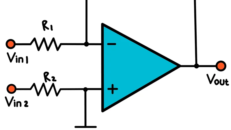
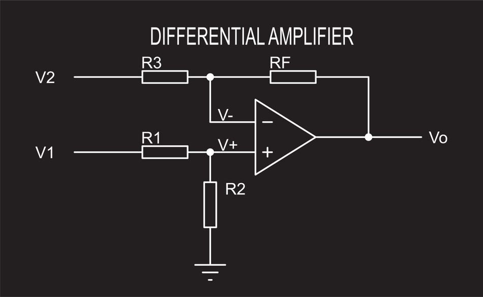
Instrumentation and Differential Amplifiers
A difference amplifier amplifies the voltage difference between two inputs while rejecting common-mode signals. Using four resistors, the differential gain is R2/R1, and the common-mode gain is ideally zero. Precision requires matched resistors (≤0.1%) for high CMRR.
The three-op-amp instrumentation amplifier improves on this design with input buffers and adjustable gain: Vout = (R2 / R1) * (1 + 2 * R5 / RG) * (V1 - V2)
Adjusting RG changes the gain without affecting resistor matching. This topology provides high input impedance, high CMRR, and is ideal for sensor signal conditioning.
Recommended reading: Difference Amplifier: Theory, Design, and Applications for Engineers
Voltage Follower (Buffer)
A voltage follower is a special non-inverting amplifier with unity gain (R2 = 0, R1 → ∞). The output simply tracks the input: Vout ≈ Vin
It provides high input impedance and low output impedance, isolating sources from loads, commonly used in ADC drivers and signal isolation.
Advanced Op-Amp Topics
Advanced operational amplifier designs address modern application requirements, including single-supply operation, rail-to-rail performance, high precision, and low noise. Understanding these topics helps engineers select the right device for demanding systems.
Single-Supply and Rail-to-Rail Op-Amps
Traditional op-amps operate from dual supplies (e.g., ±15 V), allowing the input and output to swing around ground. Modern portable and battery-powered systems often use single-supply operation (3 V–36 V) to reduce complexity and power consumption.
Key considerations for single-supply and rail-to-rail devices:
Input and output ranges shrink, increasing the impact of input offset voltage, bias currents, and noise.
Open-loop gain is typically lower (25,000–30,000).
Output swing usually stays within ~100 mV of supply rails.
Designers often use a midpoint reference voltage (Vref = VDD/2) and AC-coupling to maintain signal integrity.
High-Precision and Low-Noise Devices
High-precision op-amps minimize input offset voltage (µV), offset drift (µV/°C), and bias current (pA). Techniques include:
Chopper-stabilized / zero-drift: Periodically correct offset for ultra-low drift.
Auto-zero: Cancels internal DC errors to achieve near-zero offset.
Low-noise op-amps reduce thermal and flicker noise using:
Larger input transistors
Higher bias currents
JFET or MOSFET input stages for low current noise
Applications include instrumentation, medical devices, precision measurement, and sensor signal conditioning.
Recommended reading: Why JFETS are Key in Low Noise Sensor Amplification
Modern Innovations and Market Trends
The operational amplifier market is growing due to consumer electronics, automotive, industrial automation, IoT, and telecom. Key trends:
Miniaturization and energy efficiency for portable devices
Low-voltage and rail-to-rail designs for battery-powered electronics
High CMRR, EMI protection, and wide temperature range for automotive and industrial applications
High-speed and ultra-low-power op-amps for edge computing and IoT sensors
Recent devices illustrate innovation across the spectrum:
STMicroelectronics TSB952: Dual op-amp, 4.5 V–36 V supply, 26 V/µs slew rate, 52 MHz gain-bandwidth, automotive-grade.
Texas Instruments OPA4391: Quad precision, 45 µV offset, 1 MHz GBW, 23.5 µA supply, low drift.
Rohm LMR1901: Single op-amp, ultra-low power 160 nA, 0.55 mV offset, 1.7 V–5.5 V supply for IoT sensors.
These innovations enable engineers to select high-speed, low-power, or precision op-amps based on application, supply voltage, required bandwidth, and accuracy.
Practical Design Considerations
Designing robust op-amp circuits requires careful attention to feedback, stability, resistor selection, layout, and supply biasing. These factors directly affect gain accuracy, noise, and frequency response.
Feedback and Stability
Feedback networks define the closed-loop gain and influence stability. Key points:
Use resistor values that balance noise and bias current errors. Very large resistors increase thermal noise, while very small resistors can overload the op-amp output.
Compensation capacitors across feedback resistors can shape frequency response and limit high-frequency gain, e.g., in differentiators.
Check phase margin via simulation or Bode plots to prevent oscillation. A phase margin ≥ 45° is recommended for stability.
Resistor Matching and Temperature Effects
In difference and instrumentation amplifiers, resistor matching is crucial for high CMRR. Use precision resistors (0.1% or better).
Temperature changes affect resistance, altering gain. Use low temperature coefficient resistors or a ratiometric design so gain ratios track variations.
Decoupling and Layout
Place supply decoupling capacitors close to op-amp pins: e.g., 0.1 µF ceramic in parallel with 10 µF electrolytic. This maintains PSRR and reduces supply noise.
Use short, wide traces to minimize inductance and avoid ground loops.
For high-speed op-amps, guard high-impedance nodes to prevent leakage.
Keep input and feedback paths away from noisy digital lines to reduce interference.
Single-Supply Biasing
Ensure input signals and common-mode voltages remain within specified ranges.
Use a midpoint reference voltage (Vref = VDD/2) buffered as a virtual ground.
AC-coupling capacitors can shift signals but introduce high-pass characteristics. Account for this in the design to maintain signal integrity.
Selecting the Right Op-Amp
Engineers must balance precision, speed, power, and cost. Typical guidelines:
Application | Key Parameters | Recommended Traits |
Sensor signal conditioning | High input impedance, low offset, high CMRR | Precision or chopper-stabilized op-amp, wide input range |
Audio pre-amplification | Low noise, low THD, sufficient slew rate | JFET input, dual supply for headroom, moderate GBW |
Motor control/power electronics | High slew rate, EMI immunity | High-voltage, fast response, rail-to-rail operation |
ADC driver / sample-and-hold | Low output impedance, flat phase response | High-speed op-amp, adequate GBW, buffer configuration |
Low-power IoT sensor node | Low quiescent current, rail-to-rail | Ultra-low-power op-amp (nA–µA) |
Automotive / industrial instr. | Wide supply, high temperature, AEC-Q100 | Automotive-grade op-amp, EMI-protected |
Applications
Operational amplifiers are versatile building blocks in analog electronics. They are used wherever signal conditioning, computation, or precise amplification is required. Key applications include:
Active Filters
Op-amps are used to implement low-pass, high-pass, band-pass, and notch filters. By combining resistors and capacitors in feedback and input paths, designers can shape frequency responses while maintaining signal isolation between stages.
Oscillators and Waveform Generators
RC or LC networks with op-amps generate sine, square, and triangular waveforms. Relaxation oscillators exploit the op-amp’s saturation characteristics to produce square waves. High-speed op-amps are preferred for high-frequency waveform generation.
Analog Computation
Op-amps perform mathematical operations in analog computers and control systems:
Summing amplifiers combine multiple inputs: Vout = -Rf * (V1/R1 + V2/R2 + …).
Integrators produce an output proportional to the integral of the input signal.
Differentiators yield the time derivative of the input signal, emphasizing high-frequency components. Compensation capacitors are often used to stabilize differentiators.
Signal Conditioning
Instrumentation amplifiers measure small differential voltages from sensors (e.g., strain gauges, thermocouples), rejecting common-mode noise.
Transimpedance amplifiers convert photodiode current to voltage in optical receivers.
Audio and Communication Systems
Op-amps provide pre-amplification, active equalization, and filtering in audio mixers, microphones, and radio receivers.
Operational transconductance amplifiers (OTAs) are used in voltage-controlled filters and oscillators.
Comparator and Threshold Detection
While dedicated comparators are optimized for fast digital switching, general-purpose op-amps can be used as slow comparators for threshold detection and zero-crossing circuits.
These applications highlight the versatility of op-amp circuits, from high-speed waveform generation to precision sensor interfacing, demonstrating why op-amps remain essential in modern electronics.
Conclusion
Operational amplifiers remain cornerstones of analog and mixed-signal electronics, enabling precise amplification, signal conditioning, and computation. Understanding the differences between ideal and real op-amps, along with parameters such as open-loop gain, slew rate, CMRR, and PSRR, is essential for designing robust, high-performance circuits. Classic configurations—inverting, non-inverting, summing, integrator, differentiator, and instrumentation amplifiers—offer predictable performance and versatility across applications from audio systems to sensor interfacing.
Looking ahead, op-amps are evolving to meet emerging demands in IoT, electric vehicles, wearable devices, and precision instrumentation. Innovations such as low-power, rail-to-rail, zero-drift, and automotive-grade op-amps enhance accuracy, reduce noise, and expand operational ranges. Integration with AI-driven analog front-ends and edge computing may unlock adaptive signal processing capabilities, making op-amps not just amplifiers but smart enablers for next-generation electronics. By applying careful feedback design, resistor matching, and supply biasing, engineers can fully exploit these devices for both current and future applications.
Frequently Asked Questions (FAQ)
What is an operational amplifier?
An operational amplifier (op-amp) is a high-gain differential amplifier with high input impedance and low output impedance. It uses external components to perform mathematical operations such as amplification, addition, subtraction, integration, and differentiation. Real op-amps have finite parameters that must be considered in design.
How does the gain-bandwidth product affect op-amp circuits?
The gain-bandwidth product (GBW) is the product of closed-loop gain and bandwidth, approximately constant for a given op-amp. Increasing closed-loop gain reduces bandwidth. For example, a 1 MHz GBW op-amp can provide a gain of 1 at 1 MHz or a gain of 100 at 10 kHz. Designers must select op-amps with sufficient GBW for the required signal frequency.
What is the difference between inverting and non-inverting amplifiers?
An inverting amplifier applies the input to the inverting terminal and provides an output inverted with gain −R₂/R₁. A non-inverting amplifier applies the input to the non-inverting terminal, producing a positive-phase output with gain 1 + R₂/R₁. Non-inverting configurations offer higher input impedance and are suitable for buffering.
When should I use single-supply versus dual-supply op-amps?
Single-supply op-amps operate from one positive voltage relative to ground, ideal for battery-powered or low-voltage systems, but have reduced input/output range and gain. Dual-supply op-amps (e.g., ±15 V) allow signals to swing around ground, providing higher performance and headroom.
Why is the common-mode rejection ratio (CMRR) important?
CMRR quantifies an op-amp’s ability to reject common-mode signals. High CMRR ensures that noise common to both inputs, such as mains hum, does not affect the output. Poor CMRR leads to errors, especially in precision instrumentation.
What are zero-drift or chopper-stabilized op-amps?
These op-amps periodically correct input offset voltage, achieving extremely low offset (µV) and drift (µV/°C). They are ideal for measuring small DC signals from sensors where offset or drift dominates error, though they may introduce chopping noise and have limited bandwidth.
References
NextPCB, “Operational Amplifiers,” How To Read Electrical Schematics, NextPCB, Dec. 2025. [Online]. Available: https://www.nextpcb.com/blog/how-to-read-electrical-schematics
P. R. Gray and R. G. Meyer, “MOS Operational Amplifier Design — A Tutorial Overview,” IEEE Journal of Solid-State Circuits, vol. 17, no. 6, pp. 969–982, Dec. 1982.
Analog Devices, Op Amp Basics, Analog Devices Training Seminar Handbook, 2003.
I. Mucha, “Current operational amplifiers: Basic architecture, properties, exploitation and future,” Springer Analog Integrated Circuits and Signal Processing, vol. 7, pp. 243–255, May 1995.
A. Atvars, D. Kostrichkin, S. Rudenko, and M. Lapkis, “Performance Analyses of the Newly Developed Operational Amplifier aRD820,” arXiv:2411.08976, Nov. 13, 2024.