Why JFETS are Key in Low Noise Sensor Amplification
Learn why JFETs are often the preferred choice for low-noise sensor interfaces.

11 Jun, 2025. 10 minutes read

In sensor-based electronic systems, noise is the invisible adversary. Regardless of the application, precision performance hinges on how effectively an amplifier preserves the integrity of the original signal.
Low-noise sensor amplification refers to the ability to faithfully boost small analog signals while introducing minimal additional noise. When sensors operate in environments demanding high sensitivity and accuracy, even a few nanovolts of noise can obscure meaningful data.
Among the available technologies for front-end amplification, the junction field-effect transistor (JFET) stands out for its inherently low-noise characteristics. With negligible gate current and extremely high input impedance, JFETs are naturally suited to working with high-impedance sources like condenser microphones, photodiodes, and quartz sensors. Compared to bipolar junction transistors (BJTs), which introduce significant shot noise through base current, or MOSFETs, which tend to suffer from higher flicker (1/f) noise at low frequencies, JFETs maintain low input noise density across a wide frequency range, often as low as 1–2 nV/√Hz.
In this white paper, we’ll explore why JFETs are often the preferred choice for low-noise sensor interfaces.
Noise in Sensor Systems
In sensor systems, minimizing noise is tantamount to ensuring accurate signal acquisition, especially when dealing with weak or high-impedance sources. Noise can originate from a variety of physical phenomena, and its impact varies depending on frequency, impedance levels, and circuit topology.
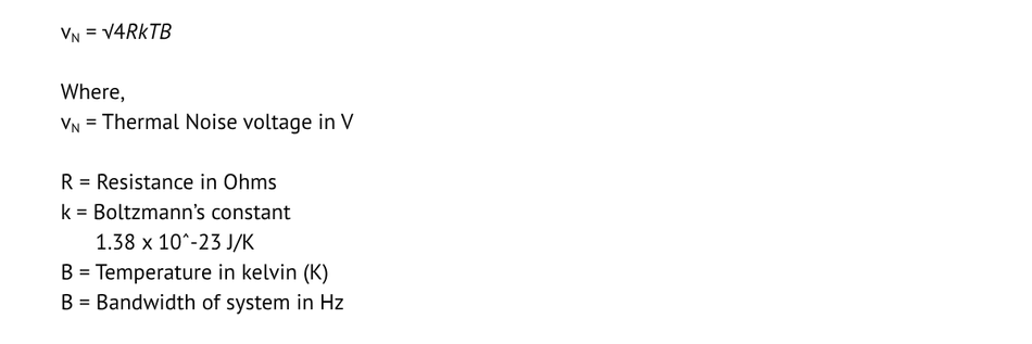
One of the most prevalent forms is thermal noise, also known as Johnson noise. It is generated by the random motion of electrons in resistive components and is proportional to both temperature and resistance. In high-impedance applications, like those involving piezoelectric sensors or photodiodes, thermal noise becomes especially problematic. As defined by Equation 1, a 10 MΩ resistor can generate over 400 nV/√Hz of noise, which can easily overwhelm a small signal unless the amplifier has a very low input noise current.
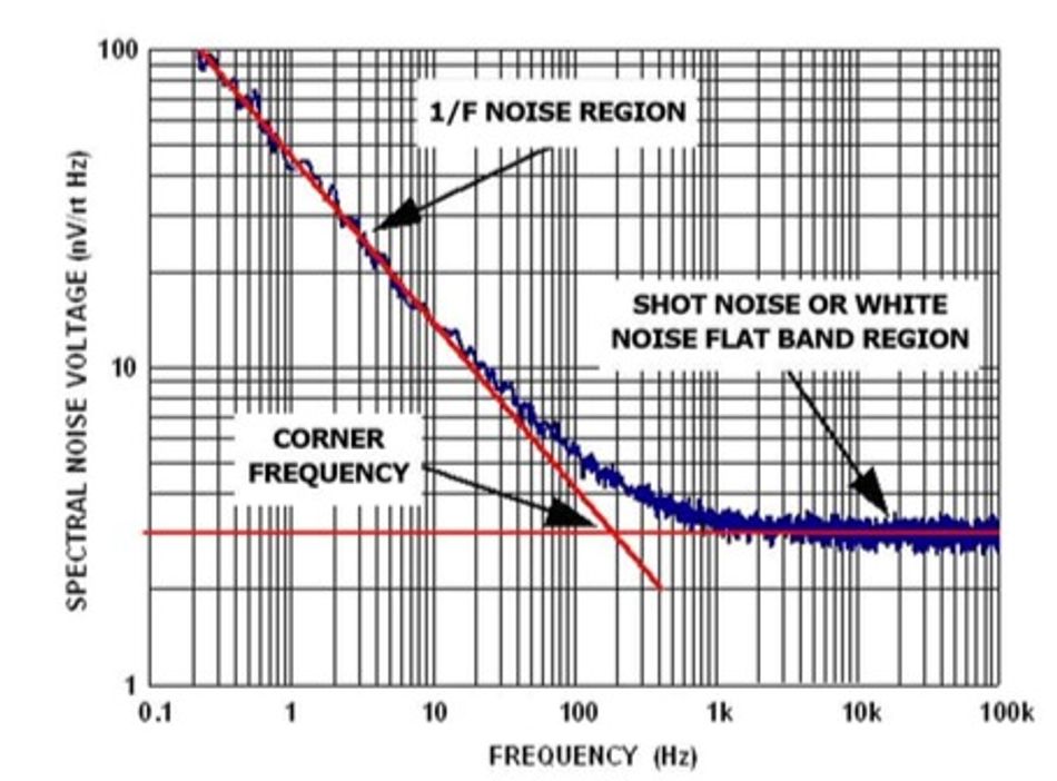
As shown in Figure 1, Flicker noise, or 1/f noise, dominates at low frequencies (i.e., below a few hundred Hertz). This type of noise originates from imperfections in semiconductor materials, such as charge traps in the substrate or defects in the lattice structure. It presents a rising noise floor as frequency decreases and can be particularly troublesome in instrumentation systems that rely on low-frequency signal components. Reducing 1/f noise requires careful semiconductor process control. Therefore, premium JFETs can excel due to advanced fabrication techniques that minimize crystal imperfections and charge traps.
Finally, shot noise arises from the discrete nature of electric charge and is most pronounced in bipolar junction transistors (BJTs) because base current fluctuations result in current noise at the input. This makes BJTs less suitable for high-impedance sources because the resulting noise current is converted into large voltage fluctuations when flowing through the source resistance.
In contrast, JFETs exhibit extremely low input bias currents that can be in the picoampere range or lower. This feature gives them a significant advantage when working with high source impedances, as they contribute far less voltage noise due to their negligible gate current. Additionally, JFETs combine low input capacitance and low voltage noise density, which helps preserve signal integrity in high-impedance and wideband applications.
Given the ubiquity of noise in electronics, low-noise design techniques are essential. Some of these techniques include minimizing parasitic capacitance, selecting optimal feedback components, and using differential circuit topologies. Starting with a component that inherently minimizes noise simplifies the challenge. In many sensor circuits, JFETs outperform BJTs and MOSFETs precisely because their device physics align more naturally with the demands of low-noise, high-impedance signal amplification.
Why JFETs Excel in Sensor Amplification
JFETs have become the go-to device in low-noise sensor amplification for a simple reason: they align perfectly with the electrical characteristics demanded by high-impedance, low-signal-level sensing technologies. Their unique combination of characteristics has made them a superior choice over BJTs and MOSFETs in precision analog front-end design.
Gate Leakage and Input Impedance
One of the defining characteristics of a JFET is its reverse-biased gate-channel junction, which results in exceptionally low gate leakage currents (i.e., sub-picoampere range). In high-impedance sensor systems, any input current can create spurious voltage drops across large source resistances. Gate leakage becomes a source of signal corruption and drift. JFETs mitigate this risk entirely and guarantee signal integrity is preserved from sensor to amplifier.
This low leakage is complemented by the ultra-high input impedance of the JFET, which is normally on the order of teraohms. This high impedance means that even tiny charge signals from capacitive sensors can be efficiently transferred to the amplifier without loss. In contrast, MOSFETs, while offering high input impedance on paper, suffer from charge injection and oxide-related leakage paths that limit their performance over time.
Low Flicker Noise
In low-frequency applications, flicker noise becomes the dominant noise source. JFETs inherently exhibit lower flicker noise than both BJTs and MOSFETs due to their bulk conduction mechanism and absence of oxide interfaces. BJTs suffer from base current fluctuations, and MOSFETs experience noise from trapped charges in the gate oxide. JFETs, by avoiding both mechanisms, achieve a flatter noise floor.
Consistent Biasing and Thermal Stability
JFETs are self-biased devices, meaning they require minimal external components to establish a consistent operating point. Self-biasing makes circuit design simpler and extends long-term stability. Whereas BJTs can exhibit large variations in current gain (β) across devices and temperature, JFETs have a more predictable drain current vs. gate voltage relationship. Their thermal behavior is also more benign as JFETs have a negative temperature coefficient for drain current. The result is a natural limit to thermal runaway and more reliable operation across wide temperature ranges.
Minimal Parasitic Capacitance
Another advantage is the low gate-to-source and gate-to-drain capacitance of JFETs.
Internal parasitics act as unwanted pathways for high-frequency signals to couple across the device, introducing phase shift, reducing gain at higher frequencies, and allowing external noise to infiltrate the signal path. High parasitic capacitance at the input stage can interact with sensor or board-level capacitance to create unintended low-pass filtering, which attenuates higher-frequency components of the signal. This limits the effective bandwidth of the amplifier and can result in slower rise times, reduced resolution in time-domain measurements, and compromised fidelity in frequency-domain analysis. In extreme cases, excessive capacitance can destabilize the feedback loop of an amplifier, leading to oscillations or ringing.
JFETs naturally offer lower parasitic capacitance compared to other transistor types because of their junction-based architecture and lack of insulating gate oxides. This means that the amplifier input can track fast signal transitions with greater precision and without being bogged down by capacitive loading. As a result, circuits built around JFETs can support higher bandwidths, better pulse fidelity, and improved signal-to-noise ratio.
JFETs vs. Other Transistor Technologies for Low-Noise Applications
When selecting the optimal transistor for low-noise sensor applications, engineers must weigh trade-offs in input noise, bias current, impedance, and capacitance. JFETs offer a compelling balance of these characteristics. Let’s compare JFETs to BJTs and MOSFETs to reveal where each technology excels and where it falls short.
JFETs vs. BJTs
BJTs operate through the movement of majority and minority carriers and require a continuous base current to remain in the active region. This base current is the source of shot noise, which becomes problematic when working with high-value resistors or high-impedance sources. For example, even a modest 0.5 pA/√Hz noise current from a BJT can result in significant voltage noise when multiplied by a 10 MΩ source impedance. In contrast, JFETs exhibit negligible gate current (i.e., often in the tens of picoamperes or lower), which dramatically reduces shot noise and makes them much more compatible with ultra-high impedance environments such as piezoelectric sensors or ion-sensitive electrodes.
Moreover, JFETs provide extremely high input impedance, typically on the order of teraohms, due to their reverse-biased gate junction. This feature ensures minimal loading of the sensor signal and eliminates the need for complex impedance buffering. While BJTs offer high transconductance, their lower input impedance and greater current noise make them less suitable for low-level signal amplification where input current must be tightly controlled.
JFETs vs. MOSFETs
Compared to JFETs, MOSFETs offer even higher DC input impedance due to the insulating oxide layer at the gate. However, this same oxide structure can introduce higher gate leakage currents over time and is prone to charge trapping, which exacerbates 1/f (flicker) noise, especially at low frequencies. In low-frequency applications such as biosensing or geophysical instrumentation, this flicker noise can dominate the signal bandwidth, severely degrading signal-to-noise ratio.
JFETs, on the other hand, exhibit significantly lower flicker noise due to their junction-based gate structure and lack of insulating layers. Additionally, JFETs maintain lower gate-to-source and gate-to-drain capacitances, which helps in dealing with fast transients or when minimizing capacitive loading.
In summary, while BJTs and MOSFETs have their place in high-speed or digital-centric designs, JFETs remain unmatched in applications requiring high impedance, low gate leakage, and minimal low-frequency noise. Their physical construction and electrical behavior make them the preferred front-end device in precision analog circuits that require signal integrity at the lowest noise floor possible.
Applications of JFETs in Low-Noise Sensor Circuits
Given their unique characteristics and suitability for low-noise sensor circuitry, JFETs are used across fields as diverse as medicine, aerospace, geophysics, and industrial automation.
Biomedical Sensors
In biomedical instrumentation, sensors must often detect extremely low-amplitude electrical signals from high-impedance sources. Examples include electrocardiograms (ECG), electroencephalograms (EEG), and electromyograms (EMG).
JFETs are a great choice for these front ends because their very low gate leakage current minimizes signal loss and prevents unwanted charge build-up, which could distort bio-signals. Their high input impedance allows accurate voltage sensing across skin-contact electrodes without drawing significant current to reduce electrode polarization effects that can skew measurements. Furthermore, low flicker noise makes JFETs especially well-suited for low-frequency biological signals that reside below 100 Hz, where many other devices suffer elevated noise.
Piezoelectric Sensors
Piezoelectric sensors are commonly used to detect pressure, vibration, and acoustic signals. These sensors generate a charge in response to mechanical stress and are extremely sensitive to input impedance and leakage paths. For this reason, piezoelectric sensors are common in applications like structural health monitoring, sonar, hydrophones, and precision accelerometers.
JFETs excel here because they prevent charge leakage at the amplifier input and allow full charge transfer and high signal fidelity. Source follower configurations are often used to buffer piezoelectric signals before further amplification to unlock both signal integrity and wide dynamic range.
Optical and Photodiode Sensors
Photodiodes convert incident light into current and require amplifiers with low bias current and low noise to avoid corrupting the photo-generated signal. In applications like spectroscopy, astronomy, industrial laser sensors, or high-speed optical communication receivers, even minor gate leakage or noise can mask the signal of interest.
JFETs provide the low leakage currents necessary to minimize dark current effects, and their low input capacitance ensures fast response and low distortion. These characteristics make JFETs a top choice in transimpedance amplifiers used with avalanche photodiodes or PIN diodes for detecting faint or high-speed optical signals.
Geophysical and Seismic Sensors
Seismic and geophysical sensors used in earthquake monitoring and down-hole drilling (e.g., oil exploration) require amplifiers that offer high common-mode rejection, minimal flicker noise, and stable performance in extreme environments up to 200°C. JFETs meet these requirements by delivering low-frequency noise performance superior to MOSFETs or BJTs, especially in differential input configurations. When paired with balanced sensor outputs and precision feedback networks, JFET-based amplifiers can maintain high resolution and dynamic range over long durations and wide temperature swings.
Industrial and Aerospace Applications
In high-reliability sectors like aerospace and advanced industrial systems, sensors must operate across wide bandwidths and resist environmental interference. Gas sensors, high-frequency accelerometers, and radiation detectors often output low-level analog signals susceptible to noise and loading effects. Here, JFETs provide the required low input capacitance, thermal stability, and rugged signal isolation to ensure accuracy under mechanical stress, radiation exposure, or high vibration. Their low power consumption and analog precision suit embedded sensing nodes that are concerned with battery life and signal integrity.
Design Considerations When Using JFETs for Sensor Amplification
Successfully deploying JFETs in low-noise sensor amplification requires careful attention to both device selection and circuit topology. While JFETs inherently offer high input impedance and low noise, their performance can vary dramatically depending on how they are biased, laid out, and integrated with surrounding components. Optimizing these elements is therefore necessary to fully harness their capabilities in precision analog front ends.
Choosing the Right JFET
Not all JFETs are created equal. Parameters such as transconductance (gm), input capacitance, and equivalent input noise voltage should be evaluated based on the application’s specific requirements.
High transconductance improves gain and bandwidth but often comes at the cost of higher input capacitance, which can degrade performance in high-speed or high-impedance applications. Input capacitance should be minimized when working with capacitive sensors like photodiodes or piezoelectric elements to prevent excessive bandwidth reduction or signal distortion. Additionally, selecting a JFET with a low noise figure (i.e., low flicker and thermal noise density) is necessary for applications where low-frequency signals dominate.
Biasing Techniques for Optimal Performance
JFETs require careful biasing to operate in the saturation region, where they deliver stable transconductance and the lowest noise. Constant-current biasing is widely used to minimize noise and ensure consistency across temperature and manufacturing variation. This technique involves using a current source or a large-value resistor to set the drain current at an optimal operating point.
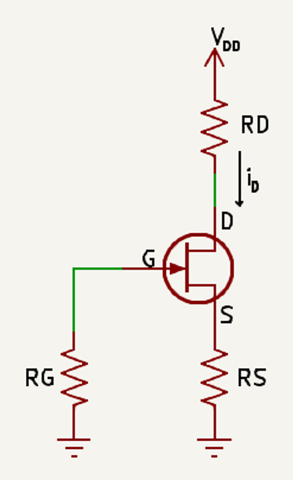
Alternatively, self-biasing using a source resistor to establish gate-source voltage offers simplicity and thermal feedback that can improve stability. However, for ultra-low-noise applications, this method can introduce additional thermal noise and may require degeneration resistance optimization to maintain signal integrity.
Minimizing Parasitic Effects
Because JFETs operate with extremely high input impedance, they are particularly sensitive to parasitic capacitances and leakage currents on the PCB. Layout must be optimized to keep gate traces short and isolated.
Guard rings driven at the same potential as the gate can reduce leakage paths on the PCB surface, and high-resistance materials should be avoided to minimize board-level noise pickup. Feedback components, like high-value resistors, should be selected for low parasitic capacitance to prevent bandwidth roll-off and instability. Additionally, care must be taken to isolate the JFET from switching nodes or digital traces, which can inject unwanted transients into the sensitive analog front end.
Cascoding for Enhanced Performance
A powerful technique for extending JFET performance is the use of a cascode configuration in which a second transistor is stacked above the JFET to hold its drain voltage constant. This mitigates the Miller effect, which otherwise multiplies gate-drain capacitance and limits bandwidth. By keeping the drain at a fixed potential, cascoding reduces effective input capacitance, enhances frequency response, and minimizes distortion. It also improves isolation between input and output stages, further preserving signal integrity in broadband or high-gain designs.
Conclusion
Sensors continue to demand ever-lower noise floors and higher resolution, engineers should not overlook the proven advantages of JFET-based front ends. Whether designing for low-frequency biomedical signals or broadband optical detectors, JFETs offer a mature yet forward-compatible solution. By thoughtfully integrating these devices into modern analog designs, engineers can unlock superior performance and measurement accuracy in even the most noise-sensitive applications.