FPGA Boards: Hardware Architecture, Toolchains, and Development Platforms
An in-depth guide to FPGA board hardware, development boards, toolchains, and selection criteria for prototyping and production.

26 May, 2026. 21 minutes read
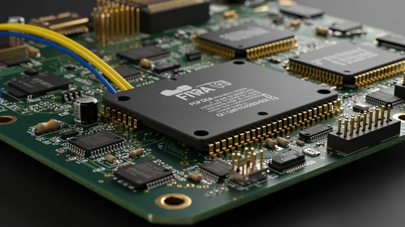
FPGA technology sits at the heart of many cutting‑edge embedded systems, from industrial control units and motor drives to AI accelerators and data centre network cards. An FPGA board makes this technology accessible by packaging an FPGA device with memory, power regulation, debug ports, and I/O connectors so engineers can experiment, prototype, and deploy reconfigurable hardware without designing a printed circuit board from scratch.
This article provides a deep dive into FPGA boards and their closely related FPGA development boards, covering theory, practical hardware considerations, and selection criteria. It serves digital design engineers, embedded systems developers, FPGA designers, and electronics students looking for a clear yet thorough overview of today's FPGA platforms.
Key Takeaways
Definition and anatomy – An FPGA board integrates an FPGA device with configuration memory, clocks, power supplies, JTAG or USB programming circuitry, user I/O, expansion connectors, and sometimes on‑board sensors or radios.
Board categories – Entry‑level and educational kits focus on ease of use; mid‑range evaluation boards provide more logic and interfaces; system‑on‑chip (SoC) boards combine FPGAs with hard CPU cores; high‑end boards offer high‑speed transceivers and large memory; low‑power boards target IoT.
Major vendors – AMD (Xilinx), Intel (Altera), Lattice, Microchip, GOWIN, and Efinix all offer devices and boards. Each ecosystem has its own toolchain (Vivado, Quartus, Radiant, Libero, etc.).
Toolchains & workflow – FPGA development involves design entry using HDL or HLS, synthesis, place‑and‑route, simulation, and configuration. Vendor toolchains like Vivado or Quartus automate these stages, while open‑source flows using Yosys, nextpnr, and Icestorm are gaining traction [14].
Selection criteria – Choosing a board requires balancing logic capacity, memory, I/O count, on‑board peripherals, transceiver bandwidth, software support, community resources, and budget.
Applications & trends – FPGA boards enable hardware acceleration, digital signal processing, prototyping ASICs, edge AI/ML, automotive and aerospace systems, high‑speed networking, and teaching digital logic. Emerging trends include heterogeneous integration, RISC‑V SoC FPGAs, and fully open‑source design flows.
Introduction
Field‑programmable gate arrays (FPGAs) are semiconductor devices whose logic structure can be reconfigured after manufacturing. Unlike microcontrollers, which execute software on a fixed CPU architecture, FPGAs implement custom hardware architectures using programmable logic blocks and configurable interconnects, described in hardware description languages (HDLs) such as VHDL or Verilog. Their highly parallel logic and reconfigurability make them ideal for digital signal processing, high‑speed interfaces, and hardware acceleration. However, working directly with bare FPGA chips requires specialist PCB design and costly hardware – hurdles that FPGA boards remove.
This article provides an engineering reference for FPGA boards and FPGA development boards. It begins by defining what these boards are and how they differ from microcontroller boards. The article then examines the anatomy of a typical board, classifies board categories, and reviews products from major vendors. A section on toolchains covers design flows using vendor software and open‑source alternatives. Selection criteria and common applications are then discussed to help readers choose the right board for their projects. The article concludes with a look at emerging trends and includes a FAQ section for quick reference.
What Is an FPGA Board?
An FPGA board (or FPGA development board) is a printed circuit board that contains a field‑programmable gate array integrated circuit along with the components needed to power, configure, and interact with the FPGA. Key components include:
FPGA fabric – The chip itself consists of a grid of configurable logic blocks (CLBs) that contain look‑up tables (LUTs), flip‑flops (FFs), distributed RAM, and multiplexers, along with dedicated digital signal processing (DSP) slices and block RAM. The quantity of logic elements or LUTs defines the size of the device. For example, the Artix‑7 FPGA on the Basys 3 board provides 33280 logic cells with 90 DSP slices and 1.8 Mbit block RAM [1].
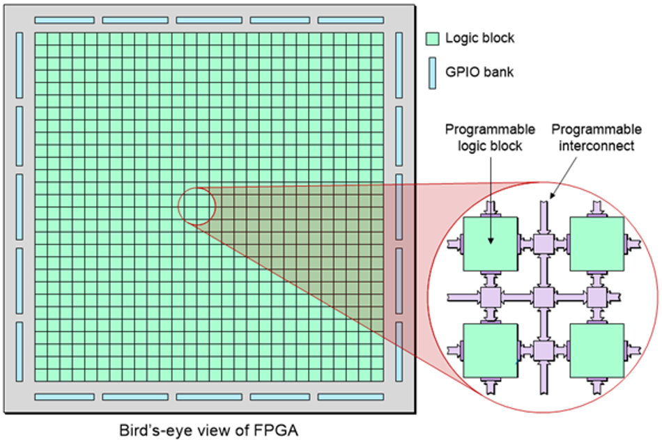
Configuration memory – FPGA configuration data (bitstream) is stored in on‑board flash memory or loaded from a host through JTAG/USB at power‑up. Some boards provide both non‑volatile flash and removable SD cards.
Power management – Switching regulators and power rails generate the core voltage (e.g., 1.0 V), I/O voltage (1.2–3.3 V), and auxiliary rails required by the FPGA and peripherals. Good regulation and sequencing are critical for device reliability.
Clocking – Crystal oscillators or MEMS oscillators provide base clock sources. Phase‑locked loops (PLLs) or mixed‑mode clock managers multiply or divide these to generate system clocks. High‑end boards include programmable clock generators or multi‑gigahertz reference clocks.
Programming interfaces – A JTAG or USB interface allows downloading bitstreams and debugging. Many boards integrate USB‑JTAG bridges, such as the Digilent USB‑JTAG used on the Basys 3 and Arty boards [1]. Others use the FTDI FT2232H dual‑interface USB bridge to support both JTAG and serial UART.
I/O connectors – General‑purpose I/O pins are routed to connectors such as PMOD headers (Digilent standard: 6-pin variant with 4 GPIOs or 12-pin variant with 8 GPIOs), Arduino‑shield headers, mikroBUS, Raspberry Pi 40‑pin headers, or high‑density FMC/HSMC connectors on professional boards. These connectors allow attaching sensors, high‑speed ADC/DAC mezzanines, Ethernet PHYs, and custom breakout boards.
On‑board peripherals – Many boards include DDR memory (DDR3/DDR4 SDRAM) for high‑throughput data buffering, flash memory for boot code, user LEDs, switches, buttons, and sometimes analog-to-digital converters, HDMI/VGA video outputs, or Ethernet PHYs.
FPGA vs MCU Development Boards
Microcontroller (MCU) development boards typically feature a CPU core, flash program memory, and RAM integrated on a single chip, along with programmable I/O peripherals. They execute sequential software instructions but cannot implement arbitrary logic. FPGAs are blank slates for hardware design: the engineer creates a hardware description (in VHDL, Verilog, or a high‑level language) that defines the circuit implemented in the logic fabric.
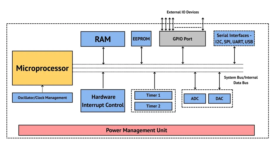
FPGA boards provide concurrency and deterministic timing at the cost of a steeper learning curve and longer design iteration cycles. Many SoC boards combine both worlds by integrating ARM or RISC‑V cores with FPGA fabric, enabling software‑programmable control with hardware acceleration.
Recommended Reading: FPGA vs Microcontroller Understanding the Key Differences and Use Cases
Anatomy of an FPGA Board
To appreciate different board offerings, it is helpful to examine the anatomy of a representative FPGA board.
FPGA Device
The FPGA chip dominates the centre of the board. Characteristics vary widely across families:
Logic capacity – specified in terms of logic cells or LUT/FF pairs. Entry boards like the iCEstick use the iCE40HX1K device with roughly 1280 logic cells and 64 Kbits RAM [7], while the Sipeed Tang Primer 25K board uses a GOWIN GW5A‑LV25MG121 FPGA with 23040 LUT4s and 23040 flip‑flops [8]. Mid‑range boards like the Arty A7 feature an Artix‑7 XC7A100T FPGA providing 101440 logic cells and 240 DSP slices [2]. High‑end boards may offer hundreds of thousands of LUTs and multi‑gigabit transceivers.
Block RAM and memory controllers – Many FPGAs include dedicated block RAM and, in more advanced devices, external memory controllers. The Arty S7-50's Spartan‑7 FPGA contains 2.7 Mbit block RAM [3]. SoC devices integrate DDR controllers; for example, the Zynq‑7020 on the ZedBoard has an ARM subsystem with a hard DDR3 controller supporting 512 MB DDR3 on the board [5].
DSP slices – Multiply‑accumulate units support high‑speed arithmetic. The Basys 3 offers 90 DSP slices [1], while the Arty A7 provides 240 DSP slices [2]. High‑end devices like UltraScale+ can include thousands.
Transceivers – For high‑speed serial interfaces (PCIe, 10‑40 Gbps Ethernet), high‑end FPGAs include multi‑gigabit transceivers (MGTs). These require careful PCB layout and are rarely found on entry‑level boards.
Memory and Storage
Most FPGA boards include external memory:
DDR3/DDR4 SDRAM for buffering large datasets or running soft processors. The Arty A7 includes 256 MB DDR3L memory [2], while the PolarFire SoC Discovery Kit features 1 GB DDR4 system memory [10]. High‑end boards may offer multiple GB of DDR4 or HBM.
On‑board flash stores bitstreams and user data. Many boards use quad‑SPI flash (8–128 Mbit). The Tang Primer 25K integrates 64 Mbit NOR flash [8].
SD or microSD slots allow removable storage; the PolarFire SoC Discovery Kit includes a micro‑SD interface [10].
Power and Clock Management
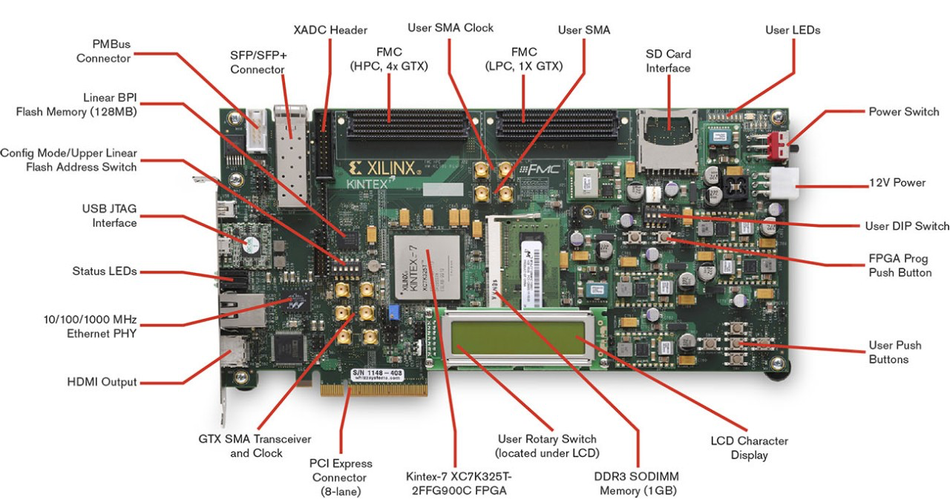
FPGA boards generate multiple voltage rails: a core rail (~1.0 V) for the logic fabric, an auxiliary rail (1.8 V) for internal circuits, and I/O rails (2.5 V or 3.3 V) for peripherals. Boards with DDR memory add a dedicated termination rail. These rails must power up in a specific sequence — if supplies come up out of order, protection diodes inside the FPGA can be forward-biased, risking latchup or permanent damage. Onboard switching regulators and sequencing logic handle this automatically. Input power is accepted via USB (5 V, sufficient for entry-level boards) or an external DC jack (typically 7–15 V).
Clock management is handled by dedicated Clock Management Tiles (CMTs) inside the FPGA. On AMD/Xilinx 7-series devices, each CMT contains a PLL and a Mixed-Mode Clock Manager (MMCM), which takes a reference clock and generates new clocks with programmable frequencies, phases, and duty cycles. A crystal or MEMS oscillator on the board — commonly 100 MHz on mid-range development boards — feeds these CMTs. High-end boards add programmable clock generator ICs or multi-gigahertz references for transceiver applications
Programming and Debug Interfaces
Programming interfaces vary by board:
JTAG/USB programmer – Many boards integrate a USB‑JTAG bridge (e.g., Digilent USB‑JTAG). Low‑cost boards may rely on external programmers (e.g., J‑Link, FlashPro).
UART/Serial Console – On‑board USB‑UART bridges provide serial consoles for soft processors. The iCEstick uses an FTDI FT2232H dual‑interface that supports programming and UART [7].
Debug LEDs and pushbuttons – Boards typically have multiple user LEDs and pushbuttons for simple I/O. The Tang Primer 25K includes two buttons, three PMOD connectors, and multiple user LEDs [8].
Expansion connectors – PMOD (Digilent) connectors carry eight single‑ended I/O. MikroBUS, Raspberry Pi 40‑pin, and Arduino connectors offer compatibility with a wide ecosystem of shields and mezzanines. High‑density FMC/HSMC connectors on professional boards support high‑speed DAC/ADC or gigabit transceiver mezzanines.
Recommended Reading: FPGA Architecture: A Comprehensive Guide for Digital Design Engineers
Types of FPGA Boards
FPGA boards can be grouped into broad categories based on their capabilities and intended use cases.
Entry‑Level and Educational Boards
These boards prioritize affordability and simplicity, making them ideal for students and hobbyists learning digital logic. They typically use small FPGAs with modest logic capacity and include user I/O for experimentation.
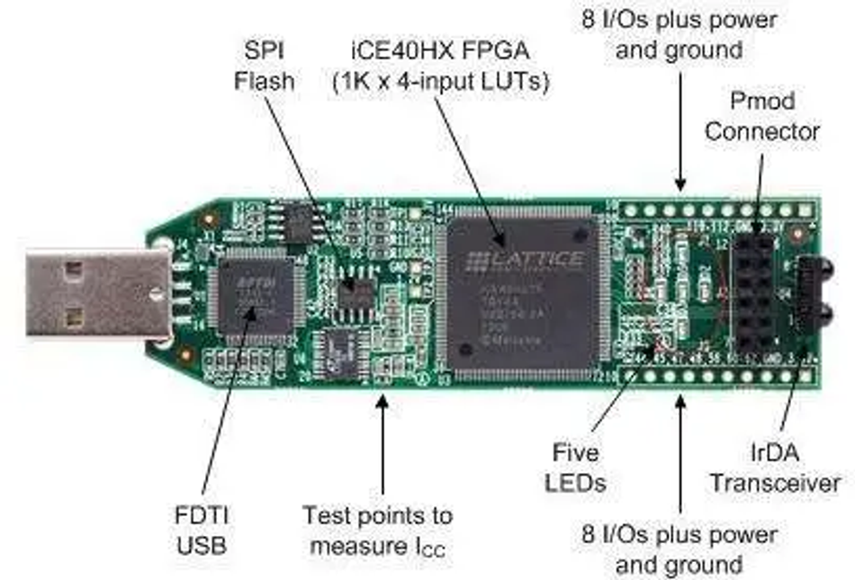
Lattice iCEstick – This USB-thumb-drive-sized board hosts the iCE40HX‑1k FPGA with roughly 1280 logic cells, 64 Kbits of embedded RAM, and 32 Mbit of SPI flash [7]. It features a Vishay TFDU4101 IrDA transceiver, five user LEDs, a PMOD connector, and an FTDI 2232H for programming and a UART [7]. The board is powered by USB and supports open‑source toolchains (IceStorm, Yosys, nextpnr).
Basys 3 – Designed for introductory courses, the Basys 3 uses a Xilinx Artix‑7 XC7A35T FPGA with 33280 logic cells, 90 DSP slices, and 1.8 Mbit block RAM [1]. It includes 16 switches, 5 buttons, 16 LEDs, a four‑digit seven‑segment display, VGA output, USB‑UART, and four PMOD connectors[1].
Sipeed Tang Primer 25K – Based on the GOWIN GW5A‑LV25MG121 FPGA with 23040 LUTs, this small board provides 64 Mbit NOR flash, 180 Kbit distributed SRAM, 1,008 Kbit block RAM, and 28 DSP multipliers [8]. It offers high‑speed JTAG+UART over USB‑C, a USB‑A host port, three PMOD ports, and a compact 64×40 mm form factor [8].
Mid‑Range Evaluation Kits
These boards balance cost and capability, making them suitable for professional prototyping and academic research.
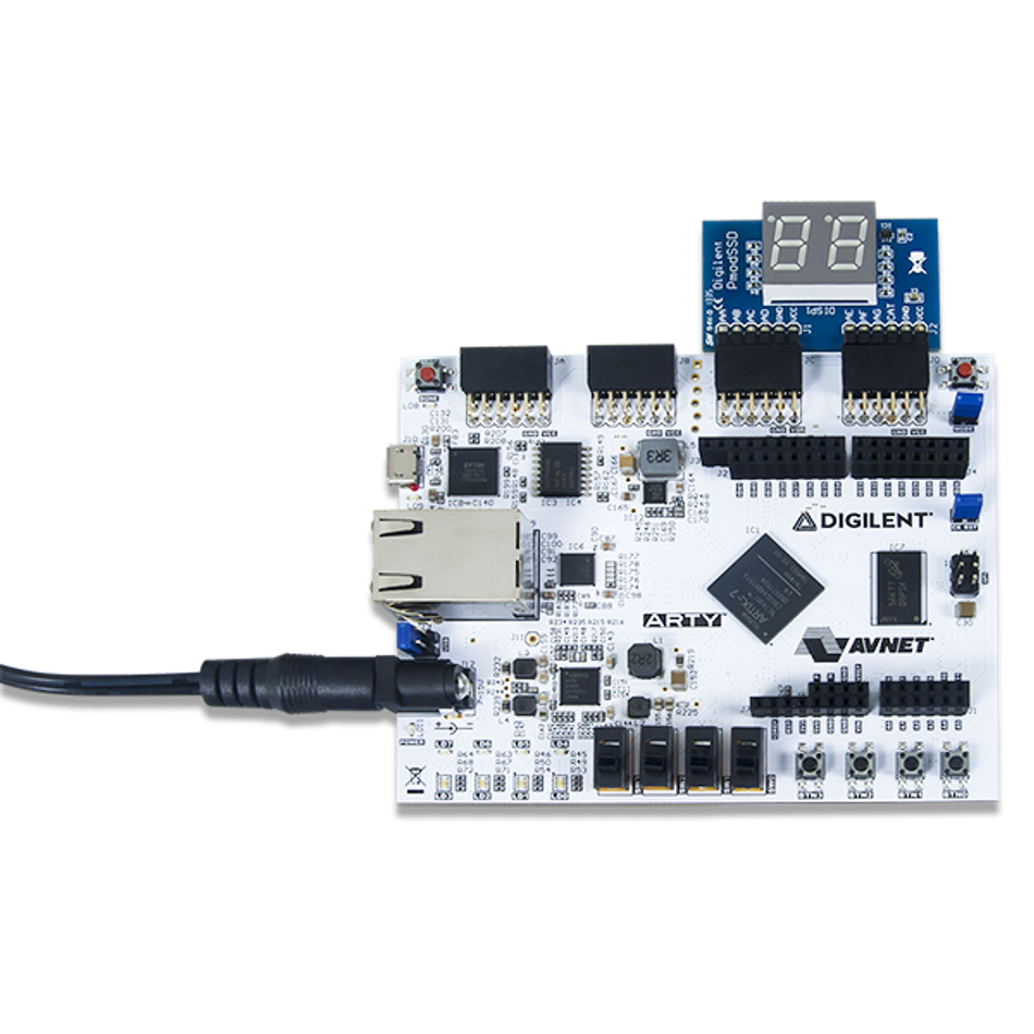
Arty A7 – The Arty A7‑100T variant features the XC7A100T FPGA with 101440 logic cells, 240 DSP slices, and 4.86 Mbit block RAM [2]. The board provides 256 MB DDR3L memory, 16 MB quad‑SPI flash, Ethernet, USB‑UART, four PMOD connectors, and an Arduino shield header [2].
Arty S7-50 – A cost‑optimized Spartan‑7 board with 8150 slices, 120 DSP slices, and 2700 Kbits or 337.5 KB block RAM [3]. It includes 256 MB DDR3L memory, 16 MB quad‑SPI flash, Ethernet, and multiple PMOD/Arduino headers [3].
Efinix Trion T20 Development Kit – The Trion T20 FPGA provides 19,728 logic elements, 1,044.48 Kbit of RAM across 204 blocks, and 36 multipliers [9]. The development board adds eight LEDs, three pushbuttons, SPI and JTAG headers, multiple I/O headers, LVDS headers, and 256 Mbit SDR SDRAM [9].
SoC FPGA Boards
System‑on‑chip boards embed a hard processor subsystem alongside FPGA fabric, enabling software applications to run alongside custom hardware accelerators.
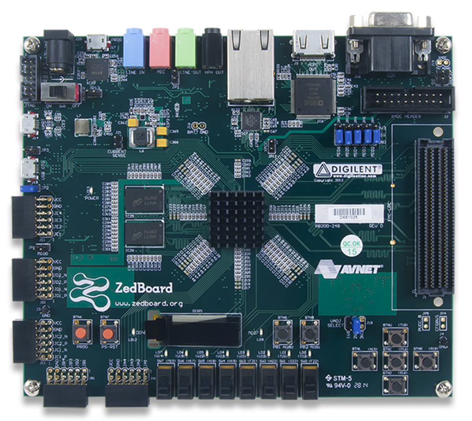
ZedBoard – Uses a Xilinx Zynq‑7000 XC7Z020 SoC with 85000 logic cells, 4.9 Mbit block RAM, and 220 DSP slices [5]. The board includes 512 MB DDR3, 256 MB quad‑SPI flash, Ethernet, USB OTG, USB‑UART, HDMI, 12-bit VGA, and expansion connectors (FMC, PMOD) [5].
DE10‑Nano – Built around the Intel/Altera Cyclone V SoC with dual‑core ARM Cortex‑A9 and 110000 logic elements [6]. The kit provides 1 GB DDR3, USB‑Blaster II JTAG, 128 Mbit flash, HDMI output, two 40‑pin GPIO headers, an Arduino‑compatible header, and gigabit Ethernet [6].
PolarFire SoC Discovery Kit – Combines a 95 K logic‑element PolarFire MPFS095T FPGA with four 64‑bit RISC‑V cores, 1 GB DDR4 memory, gigabit Ethernet, three UARTs, a micro‑SD slot, and connectors for Raspberry Pi and mikroBUS [10]. Eight debug LEDs, two pushbuttons, and eight DIP switches ease testing are also included [10].
Kria KV260 Vision AI Starter Kit – An AMD/Xilinx board featuring a Zynq UltraScale+ MPSoC with over 1200 DSP slices and UltraRAM blocks. It includes 4 GB LPDDR4, 512 Mbit QSPI boot memory, multiple MIPI camera connectors, an HDMI TX/RX, Ethernet, USB‑C, and Pmod connectors [4]. The kit targets edge AI and computer vision.
High‑End and Data‑Center Boards
High‑end boards are designed for high‑speed data processing, scientific computing, and network acceleration. They feature large FPGAs (UltraScale+, Versal, Stratix 10, Agilex) with multi‑gigabit transceivers and DDR4 or HBM memory. Examples include AMD's Alveo accelerator cards and BittWare's data‑centre boards, which provide PCIe Gen 4/5 connectivity, QSFP28/QSFP56 cages for networking, and banks of DDR4 or HBM. These boards are outside the scope of entry‑level prototyping but illustrate the upper end of the spectrum.
Recommended reading: Verilog vs VHDL: A Comprehensive Comparison
Low‑Power and IoT Boards
Lattice and GOWIN offer ultra‑low‑power devices aimed at portable and battery‑powered designs. The iiCE40 LP/Ultra/UltraPlus and Certus‑NX development kits support sensor hubs and wearable devices. Their small logic footprint and 40 nm low-power CMOS process and non-volatile configuration memory allow standby power in microwatts.
Board Category Comparison
Category | Example Boards | Typical Specs & Use Cases |
Entry‑Level / Educational | iCEstick (Lattice iCE40HX‑1K), Basys 3 (Artix‑7), Tang Primer 25K (GOWIN GW5A) | Up to ~33k logic cells; on‑board LEDs, switches, simple I/O; ideal for learning HDL, blink projects, small digital circuits [1][8]. |
Mid‑Range / Evaluation | Arty A7 (Artix‑7 100T), Arty S7-50 (Spartan‑7), Efinix T20 kit | ~20k–100k logic elements; DDR3 memory, Ethernet(Arty A7 only), multiple expansion headers; suitable for embedded soft‑core processors, DSP accelerators, educational labs [2][3]. |
SoC FPGA | ZedBoard (Zynq‑7000), DE10‑Nano (Cyclone V SoC), PolarFire SoC Discovery, Kria KV260 | Hard ARM or RISC‑V cores with FPGA fabric; 85k–110k logic cells; DDR3/DDR4 memory; connectors for cameras, sensors, and networking; good for Linux‑based embedded systems, vision, AI inference [5][6][10]. |
High‑End / Data Centre | Alveo accelerator cards, BittWare boards | Hundreds of thousands of LUTs, HBM, or large DDR4, multi‑gigabit transceivers, used for HPC, trading, network offload, and AI inference. |
Low‑Power / IoT | Lattice Certus‑NX kits, GOWIN GW1N boards | 1k–25k logic cells; minimal power consumption; targeted at portable devices, sensor hubs, and simple glue logic. |
Major Vendors and Ecosystems
AMD/Xilinx
AMD's FPGA portfolio (formerly Xilinx) spans cost‑optimized Spartan‑7 and Artix‑7 devices, mid‑range Kintex-7, and high‑end Kintex UltraScale+ and Versal families. AMD provides a broad range of development boards and System‑on‑Modules (SOMs). Boards such as Basys 3, Arty S7, ZedBoard, and Kria KV260 are popular.
AMD's Vivado Design Suite integrates design entry, synthesis, place‑and‑route, simulation, and hardware debug. The suite includes features such as incremental compile and Abstract Shell — which reduce compile time for large designs — and Dynamic Function eXchange (DFX), which allows designers to modify partial regions of the FPGA while the remaining logic continues to operate [11].
The latest 2025.2 release adds further QoR improvements and device support for Versal Prime Series Gen 2 and Versal AI Edge Series Gen 2 adaptive SoCs. Vivado supports VHDL, Verilog, and SystemVerilog entry and includes an IP Integrator and hardware debug tools such as the Integrated Logic Analyzer (ILA).
Intel/Altera
Intel's FPGA division (now operating under the Altera brand following Intel's divestiture) offers Cyclone, Arria, Stratix, and Agilex families. The Quartus Prime Design Software is a multiplatform environment that handles design entry, synthesis, placement, and routing, timing and power analysis, simulation, and hardware debug. The Quartus Prime comparison infographic lists its components: platform designer, chip planner, IP base suite, fitter (place and route), timing analyzer, design space explorer, power analysis, signal‑tap logic analyzer, and simulation via the Questa*‑Intel® FPGA Edition software [12]. Quartus Prime editions — Lite, Standard, and Pro — differ in device support and features; partial reconfiguration, for example, is a Pro‑only capability.
Boards like the DE10‑Nano demonstrate the Cyclone V SoC ecosystem. Intel/Altera's Nios V soft processor — a RISC-V-based successor to the now‑deprecated Nios II — and high‑level synthesis tools provide further embedded design options.
Lattice Semiconductor
Lattice focuses on low‑power and small‑footprint FPGAs such as the iCE40, Certus‑NX, and ECP5 families. The iCEstick board uses an iCE40HX‑1k FPGA, while Certus‑NX kits target higher‑performance designs. Lattice's Radiant design software handles the full design flow and integrates Synopsys Synplify for synthesis and QuestaSim for simulation. The Radiant user guide notes that Synplify Pro quickly synthesizes HDL code for Lattice targets, while QuestaSim simulates code and Radiant implements the complete design flow on development boards [13]. Lattice also offers Diamond software for older families and Propel for soft MCU design. Open‑source flows (IceStorm, Yosys, nextpnr) support iCE40 and ECP5 devices.
Microchip Technology
Microchip's FPGA line stems from Microsemi. The PolarFire mid‑range FPGAs and PolarFire SoC devices combine low power consumption with hardened RISC‑V CPU clusters. The PolarFire SoC Discovery Kit features a 95 K logic‑element MPFS095T device, four 64‑bit RISC‑V cores, 1 GB DDR4 memory, gigabit Ethernet, three UARTs, a micro‑SD slot, and expansion connectors [10]. Microchip's Libero SoC toolchain supports design entry, synthesis, place‑and‑route, and debug. Their FlashPro5 or FlashPro6 programmer is included on many boards.
GOWIN Semiconductor
GOWIN is a Chinese FPGA vendor targeting cost‑sensitive and low‑power markets. The GW1N (LittleBee) family offers flash-based, non-volatile FPGAs with built‑in configuration flash and small LUT counts, while the GW5A (Arora V) family uses SRAM-based configuration with larger logic resources and high-speed interfaces, including 12.5 Gbps SERDES. The Tang Primer 25K board, produced by Sipeed, uses a GW5A‑LV25MG121 FPGA with 23040 LUTs and provides on‑board NOR flash, high‑speed debug, USB host, PMOD ports, and a hard-core 4-lane MIPI D-PHY TX/RX (2.5 Gbps) accessible via the SoM's BTB connector [8]. GOWIN provides the Gowin EDA toolchain for synthesis and place‑and‑route.
Efinix
Efinix's Trion and Titanium families use a Quantum® eXchangeable Logic and Routing (XLR) fabric. The Trion T20 FPGA features 19728 logic elements, 1044.48 Kbits RAM, and 36 multipliers [9]. The Trion T20 BGA256 Development Kit includes a board with eight LEDs, three pushbuttons, SDR SDRAM, SPI/JTAG headers, and LVDS connectors [9]. Efinix's Efinity software provides a complete RTL‑to‑bitstream flow and is available free of charge; kit purchase adds one year of upgrades [9].
Recommended reading: CPLD vs FPGA: A Comprehensive Technical Analysis and Implementation Guide
Toolchains and Workflow
Developing an FPGA design involves several stages: design entry, synthesis, place‑and‑route, simulation/verification, and bitstream programming. Each vendor provides integrated software, and open‑source tools are increasingly viable.
Vendor Toolchains
Vivado Design Suite (AMD) – Supports VHDL, Verilog, and SystemVerilog design entry, plus graphical block design. Vivado performs synthesis, physical implementation and timing analysis, including simulation and hardware debug via the Integrated Logic Analyzer (ILA), and offers features like incremental compile and Dynamic Function eXchange (DFX) to reduce compile times [11]. The Standard Edition is free and supports a range of devices including Artix-7, Spartan-7, selected Zynq-7000 and some Kintex-7 devices; the Enterprise Edition supports all AMD devices.
Quartus Prime (Intel) – Handles design entry, placement, and routing, timing, and power analysis and simulation. The Quartus Prime design flow includes platform designer, chip planner, IP cores, fitter, timing analyzer, Design Space Explorer, power analysis and the Signal Tap logic analyzer [12]. Pro Edition adds partial reconfiguration and multiprocessor compile support.
Radiant (Lattice) – Combines Synopsys Synplify for synthesis, QuestaSim simulation, and Radiant implementation. The Radiant manual notes that Synopsys Synplify quickly synthesizes HDL code, QuestaSim simulates and Radiant implements the complete design flow on Lattice FPGA boards [13].
Libero SoC (Microchip) – Supports PolarFire, PolarFire SoC, SmartFusion, and other families. Libero provides mixed‑language design entry, synthesis, placement, and routing, and simulation. A FlashPro programmer (version 5 or later) connects to the device via a 10-pin JTAG header and can be used standalone or integrated within Libero SoC.
Efinity (Efinix) – Efinix's IDE offers RTL‑to‑bitstream compilation with synthesis, place‑and‑route, and timing analysis. Efinity is available as a free download; purchasing a development kit additionally provides one year of software upgrades [9].
Gowin EDA – For GOWIN devices, supports VHDL/Verilog entry, synthesis, timing analysis, and bitstream generation. For GOWIN devices, supports VHDL/Verilog entry, synthesis, timing analysis, and bitstream generation. Gowin EDA is available in an Educational Edition (free, no license required, limited device support) and a Standard Edition (requires a license applied for via the GOWIN website).
Open‑Source Toolchains
A fully open‑source flow is now practical for many Lattice iCE40 and ECP5 FPGAs and experimental support exists for Xilinx Series 7 devices via Project X‑Ray. The flow typically consists of Yosys for synthesis and nextpnr for placement and routing, with device-specific backends handling bitstream generation: Project IceStorm for iCE40 devices and Project Trellis for ECP5 devices [14]. The resulting bitstream is then flashed to the board using tools such as icepack (iCE40) or ecppack (ECP5), or via the increasingly popular openFPGALoader utility which supports a wide range of boards and programmers. .
Frameworks like LiteX leverage this toolchain to build complete SoCs — LiteX is an open‑source Python‑based SoC builder and IP library built on the Migen HDL abstraction, capable of generating designs including RISC‑V systems that can boot Linux [15].
Open‑source simulation can be performed using Icarus Verilog, Verilator, or GHDL. Hardware debug and programming is achieved via USB‑to‑JTAG adapters — such as FT2232H-based programmers — in combination with tools like OpenOCD or iceprog.
High‑Level Synthesis and Languages
High‑level synthesis (HLS) translates C/C++ and OpenCL into RTL, allowing algorithm developers to target FPGAs without writing HDL directly. AMD's Vitis HLS synthesizes C/C++ and OpenCL functions into RTL and integrates directly with the Vivado Design Suite and the Vitis unified software platform. Intel's equivalent is the oneAPI DPC++/C++ Compiler, which generates RTL IP cores or full multiarchitecture binaries from SYCL/C++ kernels and integrates with Quartus Prime for bitstream generation.
Emerging hardware description languages raise the level of abstraction further. Chisel and SpinalHDL embed hardware concepts in Scala, generating synthesizable RTL. MyHDL uses Python as a hardware description language, while LiteX/Migen provides a Python DSL for SoC construction. The LiteX paper notes that its IP components are described using the MiGEn Python DSL, simplifying design and encouraging reuse [15]. These languages all target standard toolchains by generating Verilog or VHDL as an intermediate output.
Selecting an FPGA Board
Choosing the right board depends on your application and constraints. Consider the following factors:
Logic capacity and speed – Determine the required number of logic elements, block RAM, and DSP slices. Small projects (blinkers, small CPUs) fit on devices with <10 k LUTs, while digital signal processors or AI accelerators may need >100 k LUTs and hundreds of DSP slices.
External memory – Applications involving large data sets (video buffers, neural networks) benefit from DDR3/DDR4 memory. Check the memory width (32‑bit vs 64‑bit) and bandwidth.
I/O and connectors – Evaluate the number and voltage level of GPIO pins, and whether high‑speed connectors (FMC mezzanine connectors, MIPI or LVDS signaling ) are needed. For sensor interfacing, ensure compatibility with Arduino shields or PMOD modules. Boards like the Arty A7 include four PMOD connectors and an Arduino shield header [2].
On‑board peripherals – Ethernet PHYs, USB OTG, HDMI, analog input, and radios can reduce external circuitry. For example, the DE10‑Nano integrates HDMI, Arduino, and dual-pin GPIO headers along with gigabit Ethernet [6].
Processor cores – If your project requires running Linux or high‑level software, consider SoC boards like the ZedBoard or PolarFire SoC Discovery Kit, which provide ARM or RISC‑V cores with full OS support [10].
Toolchain and support – Ensure that the board is supported by a toolchain that fits your workflow and budget. Vivado and Quartus require licensing for high‑end devices, whereas Lattice Radiant is free for supported devices and open‑source flows cover iCE40 and ECP5 targets.
Community and documentation – Popular boards have extensive online communities, tutorials, and example projects. This can significantly accelerate learning and debugging.
Cost and availability – Entry‑level boards cost tens of dollars; mid‑range kits are in the $100–$300 range; SoC and high‑end boards can cost several hundred to thousands of dollars. Consider your budget relative to required features.
Applications and Use Cases
FPGAs excel in applications requiring deterministic, parallel processing and custom I/O. Some common use cases include:
Digital Signal Processing – FPGAs implement high‑throughput filters, FFTs, and video processing pipelines using DSP slices and block RAM. The DSP resources on boards like the Arty A7 (240 DSP slices) enable efficient multiply‑accumulate operations [2].
Prototyping ASICs and hardware accelerators – Engineers can emulate ASIC designs on FPGA boards to verify functionality before committing to silicon. SoC boards allow co‑simulation of software and hardware.
Edge AI and Machine Learning – Boards like the Kria KV260 with a Zynq UltraScale+ MPSoC provide 4 GB DDR4 and MIPI camera connectors to run AI inference at the edge [4]. Combined with frameworks such as Vitis AI, developers can deploy neural networks on reconfigurable logic.
Hardware Acceleration – FPGAs accelerate compute‑intensive tasks in datacentres, such as high‑frequency trading, encryption, database query acceleration and computational fluid dynamics. Alveo and BittWare cards provide PCIe interfaces to servers.
Educational & Research Projects – Entry‑level boards support teaching of digital logic, computer architecture, and reconfigurable computing. Boards with open‑source flows allow students to explore complete toolchains without proprietary licensing.
Embedded Control – FPGAs in industrial, automotive and aerospace systems handle real‑time control loops, sensor fusion and communication protocols. The ZedBoard and DE10‑Nano's hard ARM processors make them suitable for control systems with Linux support.
Retrocomputing and Gaming – Developers recreate classic computer architectures and gaming consoles on boards such as the DE10‑Nano (used in the MiSTer project) due to its large logic capacity and ARM cores.
Programming and Getting Started
To program an FPGA board, engineers typically follow these steps:
Install toolchain – Download and install the vendor or open‑source toolchain appropriate for your device.
Create design – Write RTL using VHDL, Verilog, SystemVerilog, or a high‑level language (HLS or Python DSL). Use IP libraries for peripherals such as UARTs, AXI buses, and memory controllers.
Simulate – Use the simulator within the toolchain (ModelSim, QuestaSim, Vivado Simulator) or open‑source alternatives to verify functionality before synthesis.
Synthesize and implement – Run synthesis to map the design to logic gates. Place‑and‑route assigns logic elements to physical resources and routes signals. Tools like Vivado provide reporting and suggestions to meet timing targets [11].
Generate bitstream – After successful implementation, generate a configuration bitstream. For open‑source flows, tools like icepack or ecppack create the bitstream [14].
Program the board – Use the on‑board programmer (USB‑JTAG or FlashPro) to load the bitstream into configuration memory. Some boards support drag‑and‑drop programming over USB.
Debug – Use logic analyzers (ChipScope/Signal Tap), virtual I/O consoles, or integrated debuggers to observe signals and troubleshoot issues.
Iterate – Hardware design is iterative; adjust your design, re‑synthesize, and re‑test until performance and functionality meet requirements.
Newcomers should start with simple "blinky" projects to understand the workflow and then progress to soft processors like MicroBlaze (Xilinx), Nios V (Intel), or RISC‑V cores built with LiteX. Many boards provide reference designs, such as a FIR filter demo for the PolarFire SoC Discovery Kit, to help users learn board‑specific interfaces [10].
Conclusion
FPGA boards open the world of reconfigurable logic to a wide audience. By integrating FPGAs with power management, memory, debug interfaces, and user I/O, these boards remove the barriers to entry for digital designers and enable rapid prototyping. Entry‑level boards like the iCEstick and Basys 3 make excellent teaching platforms, while mid‑range evaluation kits like the Arty A7 and Trion T20 provide enough resources for soft‑core processors and DSP applications. SoC boards such as the ZedBoard, DE10‑Nano, and PolarFire SoC Discovery Kit merge programmable logic with hard ARM or RISC‑V cores for mixed‑software/hardware systems. High‑end accelerator cards demonstrate the FPGA's potential in data-centres and AI.
Selecting the right board involves balancing logic resources, memory, I/O, tool support, and budget. Engineers should also consider toolchain ecosystems: proprietary suites like Vivado and Quartus offer advanced features and device coverage, whereas open‑source flows using Yosys and nextpnr foster transparency and customization. Emerging trends such as heterogeneous integration (chiplets), RISC‑V hard processors, AI accelerator fabrics and fully open‑source design methodologies will continue to reshape the FPGA landscape. With careful selection and a solid understanding of the underlying technology, FPGA boards empower engineers to build innovative hardware systems that bridge the gap between software flexibility and hardware performance.
FAQ
What is an FPGA development board used for?
An FPGA development board provides the infrastructure needed to configure and use a field‑programmable gate array without designing custom hardware. The board integrates power supplies, configuration flash, clocks, programming interfaces, and I/O connectors. Engineers use it for learning digital design, prototyping custom logic, accelerating algorithms, and developing embedded systems.
How does an FPGA board differ from a microcontroller board?
Microcontroller boards have a fixed CPU executing sequential code stored in ROM, whereas FPGA boards implement custom hardware circuits configured at the logic block/LUT level. This allows FPGAs to achieve massive parallelism and deterministic timing. Many SoC FPGA boards combine hard CPU cores with programmable logic for hybrid hardware/software systems.
What programming languages can I use with FPGA boards?
The primary languages for FPGA design are hardware description languages (HDLs) such as VHDL, Verilog, and SystemVerilog. High‑level synthesis tools accept C/C++ or OpenCL and convert them to RTL. Chisel and SpinalHDL use Scala; Migen uses Python. When using open‑source flows, LiteX and Migen can build soft‑core SoCs [15].
Can I program FPGAs with open‑source tools?
Yes. For Lattice iCE40 and ECP5 devices, you can use an open‑source toolchain comprising Yosys for synthesis, nextpnr for placement and routing, and Icestorm/Project Trellis for bitstream generation [14]. Experimental support exists for some Xilinx Series 7 FPGAs via Project X-Ray Tools, as LiteX builds upon this flow to create complete SoCs. However, for many high‑end devices, you still need vendor tools.
What are SoC FPGA boards?
System‑on‑chip FPGA boards incorporate hard processor cores (ARM Cortex‑A9/A53, RISC‑V) alongside FPGA fabric. Examples include the ZedBoard, DE10‑Nano, and PolarFire SoC Discovery Kit [10]. These boards run operating systems like Linux and allow developers to offload critical functions to custom hardware accelerators in the FPGA fabric.
How do I choose between entry‑level and mid‑range boards?
Entry‑level boards are excellent for learning and small projects. They offer minimal cost and simple I/O but have limited logic resources. Mid‑range boards provide more logic cells, DDR memory, and Ethernet connectivity, making them suitable for soft processors, digital signal processing, and prototyping larger designs. Select based on the complexity of your intended projects.
What power considerations should I keep in mind?
FPGA boards require stable power with multiple voltage rails. High‑end FPGAs can draw several amperes, especially when many logic elements and transceivers are active. Consider the board's supply requirements and whether it supports USB power, barrel jack input, or both. Low‑power boards like the iCEstick draw only tens of milliamps from USB.
Do all FPGA boards support the same toolchains?
No. FPGA vendors provide their own toolchains tailored to their device architectures. AMD devices use Vivado; Intel devices use Quartus; Lattice devices use Radiant or Diamond; Microchip devices use Libero; Efinix devices use Efinity. Some boards are also compatible with open‑source flows, but you should verify support for your target device before purchasing.
References
[1] Digilent, "Basys 3 Artix-7 FPGA Trainer Board Datasheet," Digilent Inc. [Online]. Available: Link
[2] CoreEL Technologies, "Arty A7-100T FPGA Board Datasheet," C2S. [Online]. Available: Link
[3] Farnell, "Arty S7 Spartan-7 FPGA Development Board Datasheet," Farnell. [Online]. Available: Link
[4] AMD, "Kria KV260 Vision AI Starter Kit," Advanced Micro Devices, Inc. [Online]. Available: Link
[5] Avnet, "ZedBoard Getting Started Guide," Avnet, Inc. [Online]. Available: Link
[6] Intel Corporation, "DE10-Nano Kit Features," Intel Corporation. [Online]. Available: Link
[7] Lattice Semiconductor, "iCEstick Evaluation Kit," Lattice Semiconductor Corporation. [Online]. Available: Link
[8] SparkFun Electronics, "Sipeed Tang Primer 25K," SparkFun Electronics. [Online]. Available: Link
[9] Efinix Inc., "Trion T20 FPGA," Efinix Inc. [Online]. Available: Link
[10] Microchip Technology Inc., "PolarFire SoC Discovery Kit," Microchip Technology Inc. [Online]. Available: Link
[11] AMD, "Vivado Design Suite," Advanced Micro Devices, Inc. [Online]. Available: Link
[12] Intel Corporation, "Quartus Prime Edition Comparison Infographic," Intel Corporation, Nov. 2023. [Online]. Available: Link
[13] ALSE, "Installing and Discovering Lattice Radiant," ALSE. [Online]. Available: Link
[14] Signaloid, "Using the Open-Source Toolchain," Signaloid C0-microSD Documentation. [Online]. Available: Link
[15] F. Badier, J.-C. Prévotet, and F. Hameau, "LiteX: An Open-Source SoC Builder and Library Based on Migen Python DSL," arXiv preprint arXiv:2005.02506, May 2020. [Online]. Available: Link
in this article
1. Key Takeaways2. Introduction3. What Is an FPGA Board?4. FPGA vs MCU Development Boards5. Anatomy of an FPGA Board6. Types of FPGA Boards7. Major Vendors and Ecosystems8. Toolchains and Workflow9. Selecting an FPGA Board10. Applications and Use Cases11. Programming and Getting Started12. Conclusion13. FAQ