FPGA Development: Architecture, Tools, and Design Flow
Learn the architecture, toolchains, and design methodologies behind professional FPGA development — applied to DSP, embedded systems, and hardware AI.

01 Jun, 2026. 12 minutes read
Key Takeaways
Reconfigurable power: FPGAs are reconfigurable integrated circuits that implement custom hardware logic for parallel computing and deterministic timing.
Inside the FPGA: The architecture comprises configurable logic blocks, look-up tables, flip-flops, block RAM, dedicated DSP slices, and a rich routing fabric [3].
Structured workflow: Development follows a repeatable flow of design entry, functional simulation, synthesis, placement and routing, bitstream generation, and hardware testing [4].
Toolchain choices: Vendor suites like Vivado, Quartus, Radiant, and Libero provide integrated synthesis, simulation, and debugging; high-level synthesis accelerates algorithm-to-hardware conversion [5][4].
Board selection matters: Choose development boards ranging from entry-level kits to high-performance platforms based on logic resources, memory, I/O, and use case [6][7].
Emerging trends: Integrated RFSoCs, embedded FPGA, AI accelerators, and open-source toolchains are shaping the future of FPGA development [3][5].
Introduction
Field-programmable gate arrays (FPGAs) are integrated circuits that engineers can configure after manufacturing. Unlike a CPU or microcontroller that executes a fixed instruction set, an FPGA contains a fabric of configurable logic blocks (CLBs), look-up tables (LUTs), flip-flops, and programmable interconnects. These resources allow designers to implement custom digital circuits that run in true parallel processing. Modern FPGAs include on-chip memory (block RAM), dedicated DSP slices, high-speed transceivers and sometimes entire processor subsystems. Engineers describe functionality using hardware description languages (HDLs) such as VHDL, SystemVerilog, and Verilog, compile the design into a bitstream, load it onto a device, and iterate until requirements are met. Because FPGAs are reconfigurable, they shorten time to market compared with application-specific integrated circuits (ASICs) and are widely used in signal processing, embedded systems, and high-performance computing [3].
Architecture and Theoretical Foundations
Configurable Logic Blocks, LUTs, and Flip-Flops
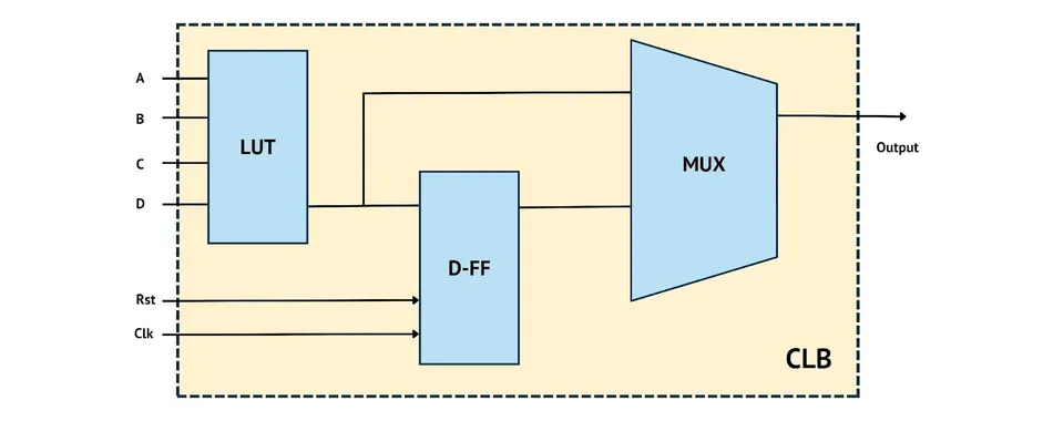
The CLB is the basic logic module in an FPGA. Each CLB contains multiple LUTs, flip-flops and multiplexers. An n-input LUT implements any Boolean function of n inputs by storing truth-table values in SRAM and selecting the output through a multiplexer. In a 3-input LUT, eight SRAM bits feed an 8:1 multiplexer [2]. A general k-input LUT uses 2^k SRAM bits and a 2^k:1 multiplexer. Modern Xilinx devices feature 6-input LUTs that can be split into two 5-input LUTs [2].In Xilinx devices, each SLICE contains eight LUTs and sixteen associated flip-flops; two slices form a CLB, giving sixteen LUTs and thirty-two flip-flops per CLB [2]. Flip-flops provide sequential storage and enable pipelining: breaking logic into smaller stages to achieve high clock frequencies. Distributed RAM, built from LUTs, can store 64 bits per 6-input LUT; larger memories use dedicated block RAM.
Memory Resources
FPGAs integrate multiple tiers of on-chip memory, each optimized for different capacity and latency requirements. Block RAM (BRAM) is the primary dedicated memory resource, implemented as synchronous dual-port storage supporting data widths up to 72 bits. Xilinx 7-series BRAM blocks provide 36 Kib of storage each, configurable as a single 36 Kib block or split into two independent 18 Kib blocks, with independent read and write clocks enabling safe data transfer across clock domains. For designs demanding higher density, AMD UltraScale+ devices introduce UltraRAM, providing 288 Kib per block and scaling to tens of MiB on a single device. Beyond dedicated block RAM, designers can construct small shallow memories using distributed RAM built from LUTs, offering lower latency at the cost of logic resources. At the top of the hierarchy, high-end platforms supplement on-chip storage with external DDR4 or High-Bandwidth Memory (HBM) for data-intensive workloads.
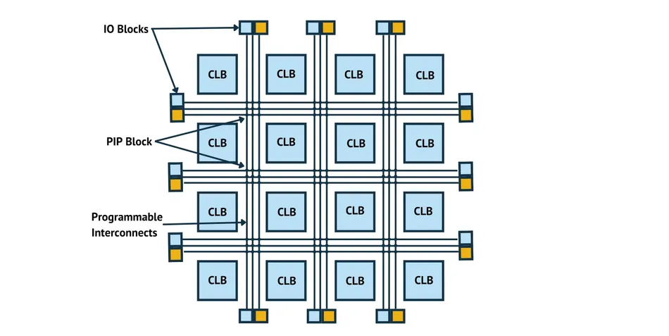
Programmable Interconnect and Routing
Configurable interconnect fabric connects CLBs, DSP blocks, block RAM, transceivers and I/O. The routing network includes local, intermediate and global segments. Placement and routing tools map the netlist onto the device, considering timing, congestion and clock domain separation [4]. Designers sometimes perform manual floorplanning to minimize critical path delays or to meet stringent timing on high-speed interfaces.
Recommended Reading: FPGA Programming: Theory, Workflow, and Practical Implementations
DSP Slices and Specialized Blocks
FPGAs include dedicated DSP slices purpose-built for arithmetic-intensive operations that would otherwise consume large numbers of general logic resources. In Xilinx/AMD devices these are called DSP48 slices; Intel refers to equivalent blocks as Variable Precision DSP blocks. AMD's 7-series DSP48E1 slice features a 25×18 multiplier, 48-bit accumulator, power-saving pre-adder, SIMD arithmetic unit supporting dual 24-bit or quad 12-bit operations, and a pattern detector — making it well suited for FIR filters, FFTs, PID controllers and fixed-point arithmetic pipelines. UltraScale and UltraScale+ devices use the DSP48E2, a superset of the DSP48E1, with an expanded 27×18 multiplier, wider 27-bit pre-adder and additional control flexibility through attributes such as AMULTSEL and BMULTSEL — extending utility to wider multiply-accumulate chains and low-precision machine learning inference.
Multiple DSP slices can be cascaded using dedicated interconnect without consuming fabric routing, enabling efficient implementation of large filters and complex arithmetic. Beyond DSP slices, most FPGA families integrate PLLs for clock generation and frequency synthesis, and multi-gigabit transceivers (MGTs) for high-speed serial protocols such as PCIe, Ethernet and JESD204B. High-end devices additionally incorporate High-Bandwidth Memory (HBM) and RF-grade ADC/DACs for memory-intensive and mixed-signal workloads.
HDLs and Module Design
Designers describe FPGA functionality using HDLs. VHDL (Very High-Speed Integrated Circuit HDL) is strongly typed and verbose, promoting disciplined design. It separates interface (entity) from implementation (architecture) and supports nine logic states defined in the IEEE 1164 standard — U, X, 0, 1, Z, W, L, H and '-' (don't care) — enabling precise simulation of uninitialized, high-impedance, and unknown signal conditions. Because of its explicitness, VHDL is common in aerospace, defence and safety-critical applications. Verilog has C-like syntax with modules, always blocks and assign statements. Its concise notation accelerates development, but weaker typing can permit subtle bugs. Both languages support modular design, enabling engineers to build reusable modules such as an adder, multiplier or memory controller and instantiate them hierarchically. SystemVerilog extends Verilog with object-oriented features and assertions for testbenches and advanced verification.
Mixed Languages and High-Level Alternatives
Many projects use mixed-language design by instantiating Verilog modules in a VHDL top-level or vice versa. High-level synthesis (HLS) allows developers to write algorithms in C/C++, SystemC, or OpenCL and automatically generate RTL code [4]. HLS improves productivity by focusing on algorithms while the tool handles resource allocation and pipelining, though hardware knowledge remains essential to guide loop unrolling, pipeline depth and memory partitioning. AMD/Xilinx's Vitis HLS (formerly Vivado HLS), Intel's oneAPI, and Microchip's HLS flows are the primary vendor tools supporting these paradigms. For Achronix devices, HLS is supported through integration with Mentor's Catapult HLS alongside the ACE place-and-route toolchain. Open-source alternatives such as Chisel (Scala-based) and PyMTL (Python-based) are widely used in academic research and custom hardware construction.
FPGA Design Flow
Creating an FPGA design is an iterative process comprising several phases:
Design entry: write the design in VHDL,Verilog, or SystemVerilog, or draw a schematic for simpler designs. Use modular coding, generics, or parameters and clear syntax to aid reuse [4].
Functional simulation: verify logic correctness using test benches and simulation tools such as QuestaSim, Vivado Simulator, Cadence Xcelium and Aldec Riviera-PRO. Simulation catches logical bugs before synthesis and accelerates development [4].
Synthesis: compile HDL into a technology-specific netlist. Synthesis tools map logic to LUTs, flip-flops, and other resources, optimize logic and apply timing constraints. [4]. Designers examine reports to check LUT usage, BRAM occupancy and DSP consumption.
Placement: assign each logical element to a physical resource. Good placement considers clock domains and reduces routing congestion [4].
Routing: connect elements via programmable interconnect. The tool balances path length and delay to meet clock frequency targets and minimize skew [4].
Bitstream generation: produce a bitstream that configures the FPGA with the synthesized design [4].
Programming and testing: load the bitstream onto the board via JTAG or USB. Run hardware tests, capture signals with integrated logic analyzers, and iterate through simulation and synthesis until timing closure is achieved [4].
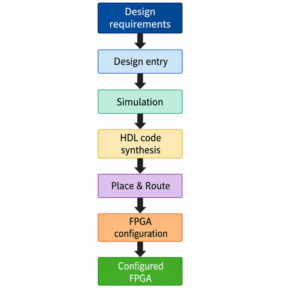
Throughout this flow, engineers must set clock constraints, analyze timing reports, and optimize routing and resource usage. Iterations are typical; changing one module may require re-synthesis and re-routing. Debugging uses signal probes, integrated logic analyzers (ILA), virtual I/O modules, and test benches. Tools like Vivado, Quartus Prime, Radiant, Libero, and Ace provide integrated environments for compiling, simulating, timing analysis, and debugging [5][4]. Open-source toolchains such as Yosys and nextpnr are gaining popularity, particularly in academic and hobbyist communities, with Yosys handling synthesis and nextpnr handling placement, routing and bitstream generation.
High-Level Synthesis and Optimizing FPGA Design
High-level synthesis converts algorithmic descriptions into RTL. HLS is particularly attractive for DSP and machine-learning workloads because engineers can express algorithms using loops and function calls. To obtain efficient hardware, designers apply optimization directives: loop unrolling, pipelining, dataflow partitioning, and resource sharing. These directives tune latency, throughput, and resource consumption. Post-HLS optimization may include manual restructuring of generated RTL to meet timing or reduce logic depth.
Parallel processing is inherent to FPGAs; multiple pipelines can operate concurrently. A fully parallel 16-tap FIR filter, for example, requires 16 multipliers and 15 adders in a direct-form architecture — though symmetric coefficient designs can reduce multiplier count further by exploiting the pre-adder in DSP48E2 slices. By mapping these onto DSP48E2 slices and pipelining them, designers can process new samples every clock cycle. HLS can generate such pipelines automatically. When low latency is crucial, designers may trade throughput for latency by partially unrolling loops or using multipliers in CLBs. Routing and clock domain crossing must be considered to avoid timing violations.
FPGA Development Boards and Tools
Practical FPGA work involves selecting appropriate hardware platforms. Boards are categorized by capability:
Category | Example boards and part numbers | Key resources | Typical uses |
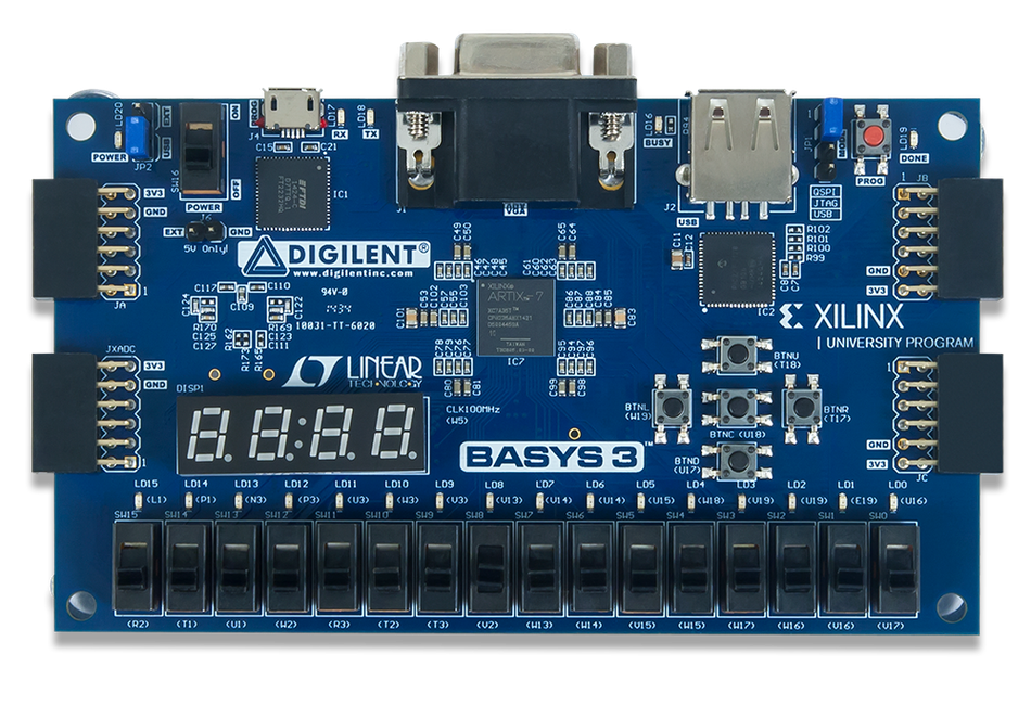
Entry-level | Digilent Basys 3 (Artix-7), Lattice iCEBreaker (iCE40), Intel DE10-Lite (Altera MAX 10 ) | 5K to 50K logic cells depending on device a few BRAM blocks, LEDs, switches, UART | Beginners, education, simple tutorials, learning HDL and test benches |
Mid-range | Nexys Video, Intel Cyclone V GX starter kit, Microchip PolarFire Eval Kit | Tens of thousands of logic cells, DDR3 memory, HDMI, Ethernet | University labs, small embedded systems, moderate DSP workloads |
High-performance | Xilinx ZCU102 (XCZU9EG), Intel Stratix 10 GX dev kit, Achronix VectorPath VP815 | ZCU102: quad-core ARM Cortex-A53 with dual Cortex-R5F, 4 GB DDR4 for processor and 512 MB DDR4 for PL, PCIe Gen2 ×4, SATA, HDMI/DisplayPort, four SFP+, two FMC-HPC [6]. Stratix 10: up to 10.2 million logic elements, 10+ TFLOPs DSP, up to 56 Gbps transceivers [7] | Prototyping for high-performance computing, real-time vision, network processing, AI acceleration |
The ZCU102 board combines a Zynq UltraScale+ MPSoC (XCZU9EG) with quad-core ARM Cortex-A53, dual Cortex-R5, Mali-400 graphics, and 16 nm FinFET logic fabric. It includes 4 GB DDR4 for the processor and 512 MB DDR4 for programmable logic, dual Quad-SPI flash, HDMI and DisplayPort interfaces, Gigabit Ethernet, four SFP+ cages, and two FMC-HPC connectors [6]. Intel's Stratix 10 GX development kit delivers up to 10.2 million logic elements, more than 10 TFLOPs of performance, and integrates ultra-fast transceivers [7]. These high-performance boards support PCIe, SATA, Ethernet, DDR4, and provide reference designs and debugging tools. Engineers use them for algorithm acceleration, network processing, real-time video, and machine learning.
Applications and Use Cases
FPGAs power a diverse range of applications:
Digital signal processing and communications: FPGAs excel at high-speed FFTs, digital up and down conversion, forward-error-correction (LDPC, Turbo codes) and beamforming. Their parallelism and deterministic timing make them ideal for 5G base stations, software-defined radios, and satellite modems [3].
Aerospace and defence: FPGAs implement radar processing, avionics protocols (ARINC 818, MIL-STD-1553), sensor fusion, and electronic warfare. The ability to update hardware via bitstream allows adaptation to new standards without replacing boards.
Automotive and ADAS: autonomous vehicles use FPGAs for sensor fusion, real-time object detection and motor control. Low-power, FPGA-based designs meet strict power budgets while providing high-performance compute.
Data centers and AI: SoC FPGAs accelerate encryption, compression, database search and inference tasks. Heterogeneous platforms integrate AI tensor engines, high-bandwidth memory and multi-gigabit transceivers to achieve low-latency processing.
Medical imaging and video processing: FPGAs enable parallel processing of high-resolution images in CT, MRI and ultrasound, performing real-time filtering, feature extraction and deep-learning inference.
ASICs Versus FPGAs
An ASIC implements a fixed function with optimal performance, area, and power. It is cost-effective in high volumes but involves long development cycles and high non-recurring engineering costs. An FPGA provides reconfigurability, allowing prototyping and field updates without fabric changes. For moderate production quantities or rapidly evolving standards, FPGAs deliver lower risk and faster deployment. SoC FPGAs combine programmable logic with embedded microprocessors (for example, ARM Cortex-A53), peripherals, and memory controllers, offering a balance between flexibility and integration. Designers may start with an FPGA for prototyping and later migrate to an ASIC for mass production. Embedded FPGA (eFPGA) cores inside ASICs offer a middle ground: small reconfigurable regions integrated into fixed logic for long-life products [3].
Recommended Reading: ASIC vs FPGA: A Comprehensive Comparison
Future Trends and Emerging Technologies
The FPGA landscape is evolving toward higher integration and heterogeneous compute. RFSoC devices integrate RF signal chains and multicore processors [3], enabling direct interfacing with wideband signals. Embedded FPGA (eFPGA) blocks bring reconfigurability into custom SoCs, reducing latency and improving efficiency [3]. UltraScale+ FPGAs built on 16 nm FinFET technology deliver 50 percent higher speed and 60 percent lower power than 7-series. Future devices incorporate AI/ML accelerators, high-bandwidth memory, multi-core processors and advanced DSP clusters. Open-source toolchains and languages such as Chisel, Amaranth HDL (formerly nMigen) and various open frameworks lower barriers for beginners and foster community contributions. As FPGAs continue to move into data centers, 5G infrastructure and autonomous systems, engineers will rely on high-level synthesis, debugging tools and iterative optimization to harness these adaptable computing platforms.
Conclusion
FPGA development combines theoretical knowledge and practical skill. Understanding how field-programmable gate arrays are built, from configurable logic blocks, look-up tables, flip-flops and programmable interconnects, helps engineers design efficient architectures. Mastery of hardware description languages such as VHDL and Verilog, along with modules, functions and rigorous simulation, leads to reliable designs. The iterative FPGA design flow of writing HDL, running test benches, synthesizing, placing and routing, and generating a bitstream is at the heart of successful projects. Using modern tools like Vivado, Quartus Prime, and high-level synthesis frameworks, designers can optimize signal processing, hardwareacceleration and real-time embedded systems. Development boards ranging from entry-level kits to high-performance platforms such as the ZCU102 and Stratix 10 allow prototyping across various domains. As technology advances with RFSoC, eFPGA and AI-centric FPGAs, the flexibility and high-performance potential of FPGA development will continue to expand. By staying grounded in solid theory and embracing evolving tools, engineers can build robust, reconfigurable systems that meet the demands of next-generation applications.
FAQ
Is FPGA development hard to learn?
FPGA development requires understanding digital logic, clocking and hardware description languages. The learning curve is steeper than software programming because you think in terms of concurrent hardware rather than sequential instructions. Many entry-level boards, online tutorials, and open-source projects make it accessible to motivated learners. Starting with simple designs, such as counters and LED controllers, builds confidence before tackling complex systems.
What programming languages are used for FPGA development?
The core languages are VHDL, SystemVerilog, and Verilog. VHDL is strongly typed and more verbose, which encourages disciplined design and is popular in aerospace and defence. Verilog has concise syntax and feels similar to C, making it common in commercial design. SystemVerilog extends Verilog with object-oriented features and assertions for verification. High-level synthesis tools also support C/C++, SystemC and OpenCL, enabling algorithm-level descriptions that synthesize into RTL code.
How long does FPGA development take?
Development time depends on project complexity and experience. Simple LED blinkers can be built in a day, while complex signal-processing pipelines or SoC-level designs may take weeks or months. The iterative flow of simulation, synthesis, place and route and timing closure often involves multiple passes. Early planning, modular design and use of vendor IP cores can reduce schedule risk. Learning the toolchain also adds time for beginners, but productivity increases rapidly with practice.
VHDL vs Verilog for FPGA development?
Both languages can describe any digital circuit. VHDL enforces strict typing, package structures and separate entity and architecture declarations. This makes it well suited to large, safety-critical projects where explicitness prevents ambiguous constructs. Verilog's concise syntax is easier for developers coming from software backgrounds and fosters rapid prototyping. Many engineers use both, choosing VHDL for top-level integration and Verilog for lower-level modules. SystemVerilog builds on Verilog to support testbench design and advanced verification.
FPGA vs ASIC vs microcontroller: how do they compare?
FPGAs are reconfigurable chips containing programmable logic and memory; they deliver parallel performance and can be updated in the field. ASICs are custom silicon optimized for a specific function, offering the best performance, power and cost in high volumes but requiring substantial non-recurring engineering and long development cycles. Microcontrollers embed a general-purpose CPU with peripherals and on-chip memory; they run sequential code and are inexpensive for control-oriented tasks. Designers choose FPGAs when flexibility and parallelism are needed, ASICs for mass-produced high-performance products, and microcontrollers for simple, low-cost control applications.
What is the best FPGA for beginners?
Beginners benefit from affordable, well-documented boards with enough resources to explore real-world designs. Popular choices include the Digilent Basys 3 (Artix-7), which offers around 33,280 logic cells, ample block RAM, a USB programmer, and built-in switches and LEDs. The Lattice iCEBreaker (iCE40) is open-source friendly, supports Yosys and nextpnr tools and costs around 60 to 80 euros. Intel's DE10-Lite (Altera MAX 10) provides similar capabilities with Quartus Prime support. These boards come with tutorials and community projects that help newcomers learn HDL and the design flow.
How much do FPGA development boards cost?
Prices vary widely. Entry-level boards like the Basys 3, iCEBreaker and DE10-Lite typically cost 50 to 150 euros and are aimed at education and hobbyists. Mid-range boards with more logic cells, memory and high-speed I/O, such as the Nexys Video or Cyclone V kits, range from 200 to 500 euros. High-performance platforms like the ZCU102, Stratix 10 GX or Achronix VectorPath can cost 1,000 to over 5,000 euros due to their large FPGAs, transceivers, memory and expansion connectors. When budgeting, consider accessories like power supplies, FMC modules and software licences.
What is high-level synthesis in FPGA development?
High-level synthesis (HLS) allows engineers to describe hardware behavior using languages like C or C++ and automatically generate RTL code. HLS tools schedule operations, partition memory and pipeline loops to produce efficient hardware. This abstracts away many low-level details, enabling designers to focus on algorithmic intent. While HLS accelerates development, understanding of hardware principles is still essential. Directives such as loop unrolling, pipelining and array partitioning guide the tool to meet timing and resource constraints. When used correctly, HLS can drastically reduce development time for DSP, machine-learning and data-flow applications.
References
[1] W. Green, "FPGA Memory Types," Project F, Aug. 24, 2020, Updated Oct. 2, 2023. [Online]. Available: Link
[2] W. Green, "Multiplication with FPGA DSPs," Project F, Nov. 27, 2021, Updated Mar. 7, 2023. [Online]. Available: Link
[3] Logic Fruit Technologies, "Understanding FPGAs: From Architecture to SoC, RFSoC and Embedded FPGA Technologies," logic-fruit.com. [Online]. Available: Link
[4] R. Jawaid, "FPGA Programming: Theory, Workflow, and Practical Implementations," Wevolver, Dec. 1, 2025. [Online]. Available: Link
[5] Fidus Systems, "FPGA Design Tools and Trends: What's New in 2025," fidus.com. [Online]. Available: Link
[6] AMD/Xilinx, "ZCU102 Evaluation Kit Product Description," Digi-Key Electronics. [Online]. Available: Link
[7] RF Wireless World, "Altera Announces Generation 10 FPGAs and SoCs," rfwireless-world.com, Jun. 10, 2013. [Online]. Available: Link [Accessed: May 25, 2026].
in this article
1. Key Takeaways2. Introduction 3. Architecture and Theoretical Foundations4. HDLs and Module Design5. FPGA Design Flow6. High-Level Synthesis and Optimizing FPGA Design7. FPGA Development Boards and Tools8. Applications and Use Cases9. ASICs Versus FPGAs10. Future Trends and Emerging Technologies11. Conclusion12. FAQ13. References