What is HBM (High Bandwidth Memory)? Deep Dive into Architecture, Packaging, and Applications
This technical article explains, what is HBM, detailing its 3D-stacked architecture, the critical role of advanced packaging, and its application in modern GPUs, AI accelerators, and embedded systems.

09 Oct, 2025. 15 minutes read
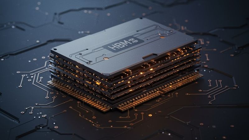
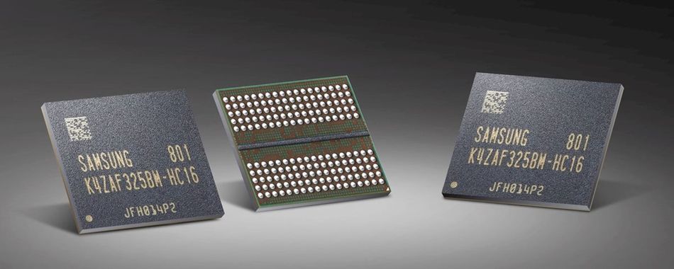
High Bandwidth Memory (HBM) Semiconductor
Introduction
The memory wall arises because processor performance grows faster than memory bandwidth. AI and HPC workloads stream enormous tensors, and conventional DDR or GDDR memory cannot keep up due to their narrow buses and high clock rates. High‑bandwidth memory (HBM) significantly widens the data path dramatically, 1024 bits in HBM3 and stacks multiple DRAM dies vertically.
But, what is HBM? In terms of architecture, this technology integrates vertically stacked DRAM dies interconnected by through-silicon vias (TSVs), providing massive parallelism without extreme clock speeds. Unlike discrete memory modules, HBM resides beside the processor on a silicon interposer, minimizing latency and improving energy efficiency. For those analyzing what is HBM in system design, its ability to deliver terabyte-per-second-class bandwidth makes it useful for AI accelerators, GPUs, and cutting edge HPC platforms.
Still, curious about, what is HBM? Let’s begin by exploring its origin and background…
Background: The Memory Wall and Widening the Bus
Modern CPUs and GPUs execute trillions of operations per second, yet their throughput is often constrained not by compute units but by memory bandwidth. Once the transistor count increases and multi-core pipelines deepen, external memory cannot deliver data fast enough—a limitation known as the "memory wall".
This performance bottleneck arises because logic density and clock speed scale faster than off-chip data transfer, leaving ALUs idle while waiting for data. Conventional DDR and GDDR memory technologies attempted to compensate by raising clock rates, but higher frequencies demand complex termination, tight impedance control, and increased power consumption.
For example, DDR5 reaches 4.8–6.4 GT/s across 16-bit channels, while GDDR6X operates near 21–22 Gb/s per pin on 32-bit interfaces. [1] Achieving 512 GB/s with GDDR6 requires several memory chips and high-speed PCB routing, introducing signal integrity and thermal challenges.
To overcome these limitations, engineers adopted a radically different approach: High Bandwidth Memory (HBM). Instead of running narrow buses at extreme speeds, HBM employs wide interfaces—1024 bits or more—operating at modest frequencies. This “wide, slow, and stacked” paradigm delivers hundreds of GB/s with lower power per bit, simplified equalization, and reduced electromagnetic interference (EMI).
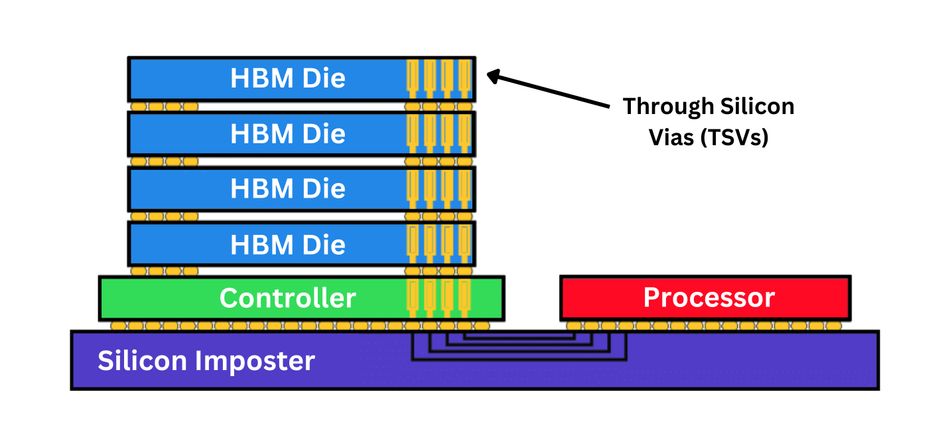
The foundation of HBM technology lies in 3D-stacked DRAM connected through Through-Silicon Vias (TSVs), vertical interconnects that pass signals through the silicon dies. Each HBM stack consists of multiple DRAM layers bonded on top of a logic die, which manages refresh, training, and data scheduling. This stack interfaces with the GPU or CPU via a silicon interposer, an advanced packaging substrate providing high-density microbump interconnects.
While 3D stacking has been explored since the early 2000s in logic-in-memory and NAND flash research, HBM represents the first JEDEC-standardized DRAM architecture to reach mass production.
HBM1, approved in 2013, debuted commercially in Fiji GPU by AMD (Radeon R9 Fury X) in 2015, pioneering stacked HBM modules on a 2.5D interposer. This design delivered 512 GB/s bandwidth at significantly lower power than GDDR5.
In 2016, Nvidia adopted HBM2 in its Tesla P100 accelerator, built for HPC and AI training workloads, marking a shift toward data center accelerators. Samsung, SK hynix, and Micron soon became key HBM suppliers, each iterating on die stacking, TSV pitch, and power efficiency.
By 2019, HBM2E pushed per-pin data rates beyond 3.2 Gb/s, while HBM3 and HBM3E now exceed 6.4 Gb/s, offering >1 TB/s bandwidth per stack. These advances enable AI accelerators, supercomputers, and next-generation GPUs to handle massive parallel workloads efficiently.
Today, high bandwidth memory has become integral to AI applications, machine learning inference, and HPC clusters, where memory bottlenecks once constrained performance. Its combination of 3D stacking, wide interfaces, and low power design positions HBM as the cornerstone of next-generation semiconductor memory architectures.
Recommended Reading: TPU vs GPU: A Comprehensive Technical Comparison
Architecture and Technology
Stack Structure and Data Organization
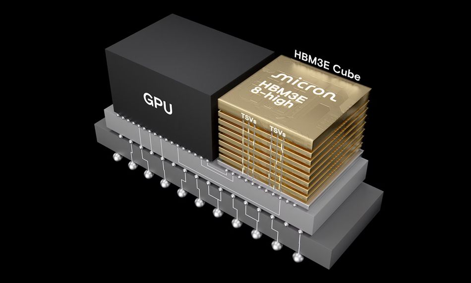
Each HBM stack combines a logic base die and multiple DRAM layers, vertically interconnected through Through-Silicon Vias (TSVs) and microbumps. The logic die integrates memory controllers, I/O interfaces, ECC management, refresh logic, and power delivery circuits. Above it, several thinned DRAM chips—typically 8 to 12—are precisely aligned and bonded to form a 3D-stacked DRAM module.
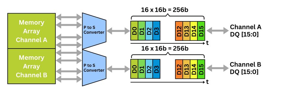
Each HBM stack exposes 16 independent 64-bit channels, allowing fine-grained access to memory banks. HBM3 enhances concurrency by splitting each 64-bit channel into two 32-bit pseudo-channels, enabling parallel command and data streams. A command bus orchestrates operations, while a data bus transfers payloads using double data rate (DDR) signaling.
Despite operating at modest frequencies, the wide 1024-bit interface yields extraordinary aggregate throughput. At 6.4 Gb/s per pin, HBM3 achieves 819 GB/s per stack—far exceeding conventional DDR5 or GDDR6 memory bandwidths. The newer HBM3E standard, developed by Micron, Samsung, and SK hynix, achieves 9.8 Gb/s, pushing bandwidth close to 1 TB/s per stack —a critical enabler for AI training, machine learning, and HPC accelerators in data centres.
Beyond raw speed, HBM memory integrates on-die ECC, fault repair, and adaptive refresh. The logic die can retire faulty pages, map defective TSVs, and dynamically retrain timing to maintain system reliability. Its decoupled clock architecture allows the command bus to run at half the data frequency, reducing jitter and improving signal margins—essential for multi-stack, high-performance deployments.
2.5‑D Packaging and Silicon Interposers
The extremely wide HBM interface — over 1000 I/O connections per stack — cannot be routed using standard organic substrates, as trace lengths would introduce delay, loss, and crosstalk. [2] Instead, HBM leverages 2.5D advanced packaging with silicon interposers that provide fine metal routing layers, low parasitic capacitance, and dense TSV arrays.
In the CoWoS (Chip-on-Wafer-on-Substrate) platform, the HBM stacks and GPU/CPU die are mounted on a passive silicon interposer, which is then attached to an organic substrate. This shortens interconnect distances, enhances signal integrity, and enables multi-terabit-per-second (Tb/s) communication between compute and memory.
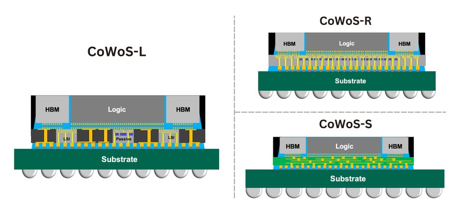
The variants include:
1. CoWoS-S: Conventional silicon interposer; high density, mainstream for Nvidia and AMD GPUs.
2. CoWoS-R: Organic interposer with redistribution layers; cheaper but with lower I/O density.
3. CoWoS-L: RDL-based design embedding active silicon bridges for larger form factors.
EMIB (Embedded Multi-Die Interconnect Bridge), offered by Intel, provides an alternative. It embeds small silicon bridges within an organic substrate to connect adjacent dies through microbumps. EMIB-T adds TSVs within the bridge, improving power delivery and signal integrity. Supporting large packages (up to 120 × 180 mm) and <45 µm bump pitches, EMIB enables multi-tile CPUs, FPGAs, and future HBM4 integration within compact footprints.
These 2.5D architectures represent the convergence of logic, memory, and interconnect technologies—paving the way for heterogeneous computing and high-bandwidth accelerators.
Recommended Reading: CoWoS Packaging Technology: Advanced Automation Systems in Modern Industrial Packaging
Standard Evolution
The HBM family has evolved through multiple generations:
HBM1 (2013) uses eight channels and runs at 1 Gb/s per pin, providing ~128 GB/s per stack. It saw limited deployment in Fiji GPUs by AMD.
HBM2 (2016) doubles the data rate to 2 Gb/s and increases capacity to 8 GB per stack. Tesla P100 by Nvidia and Vega GPUs by AMD used HBM2.
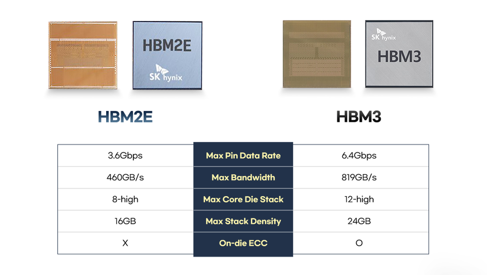
HBM2E raises the data rate to 3.2 Gb/s and supports 12–16‑high stacks, delivering up to 410 GB/s and 32 GB per stack.
HBM3 introduces 16 channels and pseudo‑channels, pushing data rates to 6.4 Gb/s and bandwidth to 819 GB/s per stack. It reduces core voltage to 1.1 V and features decoupled clocks and advanced ECC. H100 GPU by Nvidia uses HBM3 too.
HBM3E increments speeds to ~9.2–9.8 Gb/s and retains the 1024‑bit interface. Samsung demonstrated 12‑high 36 GB stacks running at 9.8 Gb/s.
HBM4 doubles the interface to 2048 bits, uses 32 channels (64 pseudo‑channels) and supports variable voltage operation. Data rates reach 8 Gb/s per pin for 2 TB/s per stack and capacities up to 64 GB. HBM4 samples by Micron in the early days deliver 36 GB and 2 TB/s bandwidth.
The future projections regarding HBM5 – HBM8 envision further increases in interface width (4096 bits to 16,384 bits) and data rates (8–32 GT/s). They may integrate on‑stack cache, CXL interfaces and embedded NAND to create hybrid memory modules.
The table below summarises key parameters across generations:
| Generation | Per-Pin Rate (Gb/s) | Interface | Channels | Bandwidth Per Stack | Capacity |
| HBM1 | 1.0 | 1,024 bits | 8 | ~128 GB/s | 4–8 GB |
| HBM2 | 2.0 | 1,024 bits | 8 | 256 GB/s | Up to 16 GB |
| HBM2E | 3.2 | 1,024 bits | 8 | 410 GB/s | Up to 32 GB |
| HBM3 | 6.4 | 1,024 bits | 16 | 819 GB/s | Up to 36 GB |
| HBM3E | 9.8 | 1,024 bits | 16 | ~1 TB/s | Up to 36 GB |
| HBM4 | 8.0 | 2,048 bits | 32 | 2 TB/s | Up to 64 GB |
The evolution of HBM technology underscores a shift toward vertical integration, massive parallelism, and energy-aware design. This enables AI, HPC, and data center workloads to overcome the memory bottleneck that once limited next-generation accelerators.
Recommended Reading: High Bandwidth Memory: Concepts, Architecture, and Applications
Packaging and Integration
Integrating HBM (High Bandwidth Memory) into modern compute systems demands tight collaboration between circuit designers, thermal engineers, and advanced packaging specialists. Unlike discrete GDDR or DDR memory modules, HBM stacks are physically co-located with the GPU or CPU on the same 2.5D substrate, dramatically shortening interconnect lengths and improving memory bandwidth per watt.
CoWoS-Based Integration
CoWoS (Chip-on-Wafer-on-Substrate) platform remains the dominant integration method for AI accelerators, HPC processors, and data center GPUs. It combines multiple HBM stacks, the processor die, and additional chiplets such as L3 cache, I/O tiles, or network-on-package dies onto a passive silicon interposer.
The interposer provides ultra-dense metal routing, TSV-based vertical connections, and fine-pitch microbumps that link each HBM stack to the memory controller of the processor. Because HBM operates on a 1024- to 2048-bit interface, these interposers must accommodate thousands of signals per stack with minimal crosstalk and parasitics.
Large-scale designs, such as MI300, which integrates multiple HBM3E stacks and Zen 4 CPU tiles, rely on reticle stitching to create interposers that exceed standard lithography limits—up to 3.5 times the reticle size. This enables unprecedented package dimensions, supporting multi-terabit-per-second (Tb/s) aggregate bandwidth across heterogeneous chiplets.
To sustain such dense power and signal networks, Power Delivery Networks (PDNs) are co-designed across the interposer and package substrate, distributing multiple voltage domains for HBM, logic, and PHY circuits. Decoupling capacitors, embedded in both the interposer and substrate, mitigate voltage droop and noise coupling, thereby maintaining power efficiency and signal integrity at multi-gigabit speeds.
Leading memory vendors, such as Samsung, SK Hynix, and Micron, collaborate with foundries to ensure that HBM3E and upcoming HBM4 stacks align mechanically and electrically with CoWoS assembly requirements. This is particularly as stack heights approach 12-high configurations and bandwidths exceed 1 TB/s.
EMIB and Hybrid Integration
EMIB (Embedded Multi-Die Interconnect Bridge) offers an alternative to full-silicon interposers. Instead of spanning the entire package, EMIB embeds small silicon bridges directly within an organic substrate, connecting neighboring dies through fine-pitch microbumps. This approach drastically reduces interposer cost while maintaining high I/O density and low latency.
The enhanced EMIB-T (TSV-enabled) version introduces through-silicon vias within each bridge to improve power delivery and return path continuity, enabling larger multi-die assemblies. EMIB-T supports reticle-sized dies, allowing over a dozen compute or memory tiles and hundreds of I/O lanes on a single organic package—ideal for HPC, AI accelerators, and data centre-grade CPUs.
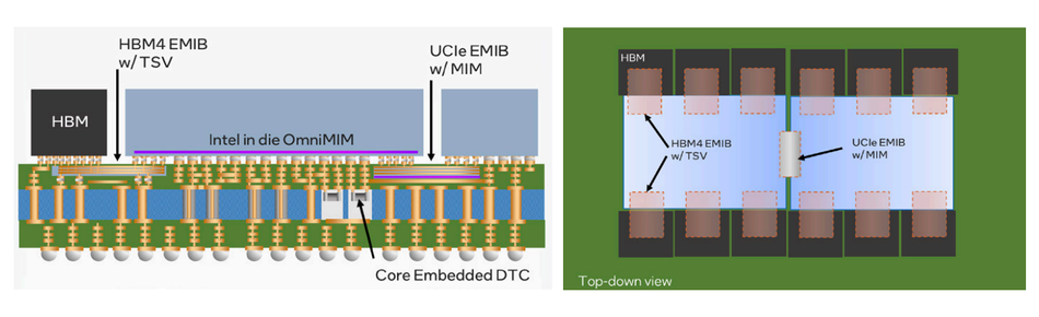
While EMIB cannot match the full routing density of CoWoS-S, its modular design simplifies yield management. It lowers manufacturing costs, particularly for complex SoCs where full-silicon interposers would be prohibitively large or expensive. Future Intel Xeon and FPGA families are expected to pair EMIB-T with HBM4 for next-generation heterogeneous compute platforms. [3]
Recommended Reading: What is High Bandwidth Memory 3 (HBM3): Complete Engineering Guide 2025
Performance in Modern Systems
The transformative role of HBM (High Bandwidth Memory) is most visible in modern AI accelerators, GPUs, and HPC architectures, where memory bandwidth has become a primary performance enabler. Let’s go through their detail:
Nvidia H100 and H200: The Hopper architecture pairs a ~814 mm² GPU die with six 16 GB HBM3 stacks on a CoWoS‑S interposer. The memory operates at 6.4 Gb/s per pin, providing a total bandwidth of 4.9 TB/s. This bandwidth is crucial for feeding the tensor cores used in AI training.
Nvidia GH200 (Grace Hopper): Combining an H100 GPU with an Arm Grace CPU and six 24 GB HBM3E stacks across a 6144‑bit interface, the HBM3E version delivers over 25% more bandwidth than the HBM3 variant. The integrated CPU reduces latency between compute and memory.
AMD Instinct MI300 Series: The MI300A merges Zen 4 CPU cores and CDNA 3 GPU cores with 128 GB of HBM3; the MI300X uses eight GPU dies and 192 GB of HBM3 to reach 5.3 TB/s of bandwidth. The unified HBM pool enables CPU and GPU cores to share memory without requiring data copying.
Micron HBM4 Samples: Micron’s 36 GB, 12‑high stacks run at ~7.85 Gb/s on a 2048‑bit bus, delivering 2 TB/s of bandwidth—about 60% higher than HBM3E and 20% more energy‑efficient. Production is targeted for 2026, with adoption expected in Nvidia’s “Vera Rubin” GPUs.
FPGAs and Networking: Xilinx (now AMD) integrated HBM into Virtex UltraScale+ FPGAs for network buffering and analytics. Broadcom’s Jericho3‑AI network switch uses four HBM3 stacks to provide deep packet buffers.
The rise of HBM has created supply‑chain challenges.
Reuters reports that HBM chips by SK Hynix are sold out through 2025, and demand is expected to grow by about 60% per year. Because packaging (CoWoS and EMIB) is complex and requires separate manufacturing lines, capacity is limited. The new Advanced Backend Fab 6 by TSMC aims to provide up to 1 million wafers per year of advanced packaging capacity, but this may still fall short of AI demand.
Design Considerations
Designers integrating HBM must address multiple interrelated challenges:
Power Delivery: The 1024‑ or 2048‑bit I/O draws large transient currents. PDN design must minimize impedance across a wide frequency range. The interposer and substrate incorporate dense power/ground grids, as well as large decoupling capacitors. Intel’s EMIB‑T integrates MIM capacitors into the bridge to improve power integrity.
Thermal Management: Stacked DRAM dies sit next to a hot logic die, creating a concentrated heat source. Packages often use vapor chambers, liquid cooling or disaggregated heat spreaders (as in Intel’s EMIB‑T) to maintain safe temperatures. Designers must balance thermal expansion across materials to avoid warpage.
Signal Integrity: Thousands of parallel lines can couple noise. Designers use matched trace lengths, differential signaling, on‑interposer termination and decoupled clocks to mitigate jitter and crosstalk. Pseudo‑channels help by reducing channel width and increasing burst length.
TSV Yield: Each DRAM (Dynamic Random Access Memory) die contains hundreds of TSVs; manufacturing defects can impact yield. HBM uses redundancy, ECC and page retirement to tolerate faulty TSVs.
Controller Tuning: Memory controllers must schedule accesses across channels, manage prefetching and handle refresh. HBM’s longer burst lengths require deeper buffering. Adaptive refresh algorithms reduce refresh penalties and improve energy efficiency.
Supply and Cost: HBM devices are expensive, and advanced packaging lines are capacity-constrained. Engineers must plan production quantities early and may need to qualify multiple suppliers (e.g., SK Hynix, Samsung, Micron).
HBM design demands a holistic co-optimization—balancing power, thermal, signal, and yield considerations while maintaining scalability and cost viability for next-generation AI, HPC, and data center platforms.
Emerging Trends and Future Directions
Next-generation HBM (High Bandwidth Memory) is evolving beyond pure storage, integrating compute, customization, and new interconnect standards.
Processing-in-Memory (PIM) Revolution
Processing-in-Memory (PIM) merges logic directly within DRAM, enabling localized computation. HBM-PIM by Samsung integrates miniature AI engines inside each memory bank, offloading matrix multiplications, convolutions, and activation functions.
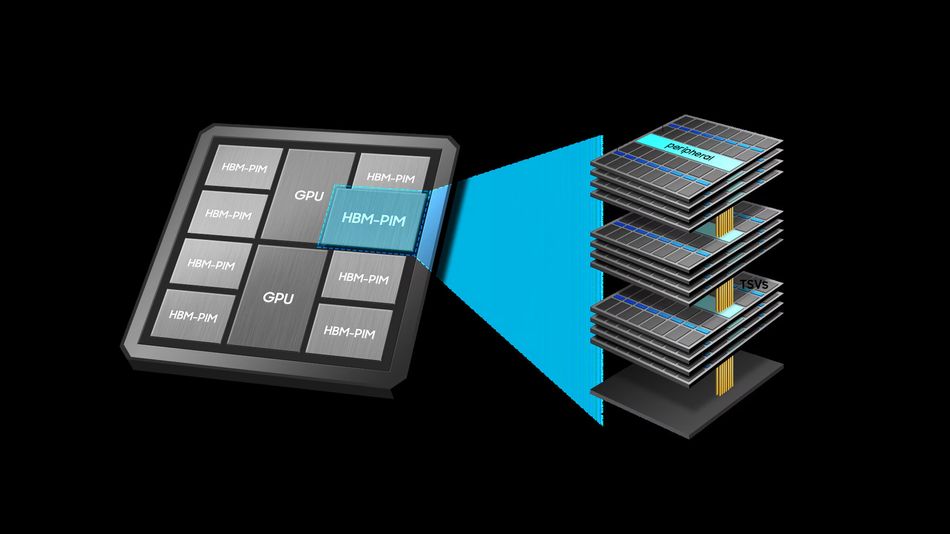
HBM-PIM can more than double system performance and cut energy consumption by over 70% compared to conventional accelerators. This approach reduces data movement between CPU, GPU, and memory, paving the way for energy-aware in-memory architectures suited for AI training and inference accelerators.
Toward HBM4E, HBM5, and Beyond
HBM4E builds upon HBM4, offering customizable logic bases and configurable interfaces to support specialized AI and data center processors.
HBM5, projected for 2029, is expected to double I/O width to 4096 bits, integrate on-stack L3 cache, and introduce CXL and LPDDR-style interfaces for memory pooling. [4] It may adopt direct hybrid bonding (replacing micro-bumps) to reduce parasitics and improve signal integrity.
Looking further, HBM6 (~2032) could achieve 16 GT/s per pin and 8 TB/s per stack, while HBM7/HBM8 may integrate DRAM with embedded NAND, forming memory-centric systems that deliver up to 64 TB/s of bandwidth—ideal for exascale AI.
Hybrid Interposers and High-Bandwidth Flash
Emerging CoWoS-L designs embed silicon bridges into organic interposers, enabling reticle-spanning packages for multi-die integration. Researchers are also exploring high-bandwidth flash, combining HBM and NAND on the same interposer to bring storage closer to compute, bridging the gap between memory and persistence in future heterogeneous systems.
Comparison with Other Memory Technologies
The unique combination of wide interface and 3‑D stacking in HBM differentiates it from conventional memory:
DDR and LPDDR modules deliver high capacity and cost efficiency, making them ideal for general-purpose computing in CPUs, servers, and mobile SoCs. However, their narrow interfaces (16–32 bits) and moderate speeds (up to 6.4 GT/s for DDR5) limit memory bandwidth. While LPDDR5X improves power efficiency, these technologies cannot sustain the throughput demanded by AI models, data center inference, or HPC workloads.
GDDR6 and GDDR7 raise per-pin data rates to 22–32 Gb/s, offering significant gains for consumer GPUs and gaming systems. Yet, they still rely on 32-bit buses, requiring multiple chips and complex PCB routing to reach several hundred GB/s of bandwidth. This scaling increases board power, signal loss, and design complexity, making GDDR suitable mainly for graphics cards and workstations where form factor and cooling are less constrained.
In On-Package Cache Memory, technologies such as 3D V-Cache by AMD or on-die SRAM by Intel provide ultra-low latency access, ideal for caching hot data close to the compute units. However, their capacities are limited to tens of megabytes, making them complementary to HBM rather than competitive.
HBM, positioned between GDDR and on-die caches, offers a mid-latency, high-bandwidth solution with per-stack capacities ranging from 36 to 64 GB in HBM3E and HBM4. Its 1024- to 2048-bit interfaces and lower operating frequencies deliver terabyte-class throughput with exceptional power efficiency. By stacking DRAM dies vertically and placing them adjacent to the GPU or CPU via silicon interposers, HBM minimises trace length, reduces power consumption per bit, and simplifies board routing.
The trade-off lies in manufacturing cost and integration complexity, but for AI accelerators, HPC systems, and data center processors, the performance-per-watt advantage makes HBM indispensable.
Recommended Reading: AI-Accelerated ARM Processors deliver truly smart IoT
Applications and Use Cases
The high bandwidth and relatively low energy per bit in HBM make it ideal for several domains:
Artificial Intelligence (AI) and Machine Learning: Deep neural networks involve large matrix multiplications and convolutions. HBM’s parallel channels feed tensor cores and SIMD units efficiently, reducing memory stalls. Training large language models (LLMs) like GPT‑4 requires feeding terabytes of data per second; HBM is essential here.
High‑Performance Computing (HPC): Applications like computational fluid dynamics, weather modeling and molecular dynamics perform intensive vector operations. HBM accelerates these by providing near‑compute bandwidth, enabling strong scaling across GPU clusters.
Data-Centre Accelerators: Products like AMD MI300A unify CPU and GPU memory in a single package, simplifying programming and improving efficiency. HBM is also used in AI inference accelerators and custom ASICs.
Networking and FPGAs: Switches like Broadcom’s Jericho3‑AI incorporate HBM stacks as deep packet buffers, offering deterministic latency and high throughput. FPGAs integrate HBM to accelerate data analytics and packet processing.
Embedded and Edge Computing: As packaging costs decrease, HBM is moving into industrial AI and autonomous systems, providing deterministic high bandwidth with moderate power. Future CoWoS‑L and EMIB‑T packages will enable smaller form factors.
By combining high bandwidth, scalable capacity, and advanced packaging, HBM is reshaping performance boundaries across AI, HPC, networking, and embedded computing. This bridges the gap between processing speed and memory access in next-generation systems.
Design Tips for Engineers
Implementing HBM (High Bandwidth Memory) demands close collaboration between system architects, packaging engineers, and foundry partners. The following best practices help optimize performance, reliability, and manufacturability in AI, HPC, and data center designs.
Engage Packaging and Manufacturing Partners early – Decide between CoWoS variants or EMIB based on bandwidth, area, cost and supply constraints. Packaging choices influence floor planning, power distribution, and thermal design.
Balance Traffic across Channels – Use memory controllers that distribute transactions evenly across channels and pseudo‑channels. Align data structures with channel boundaries to avoid hotspots.
Model Power and Thermal Behavior – Use co‑simulation tools to evaluate PDN impedance and heat dissipation. Plan for future standards (HBM3E/HBM4) with higher power densities.
Leverage Reliability Features – Enable ECC, page retirement and adaptive refresh. Monitor error statistics to detect ageing or thermal hotspots.
Plan for Supply‑Chain Constraints – HBM and CoWoS capacity is limited; secure allocations early and consider second sources (Samsung, Micron) to mitigate risk.
By aligning architecture, packaging, and supply-chain strategy early, engineers can utilize HBM to achieve high bandwidth, low power, and robust reliability across next-generation AI and HPC platforms.
Conclusion
HBM has transformed from a niche innovation into a foundational technology for AI, HPC, and data centre accelerators. By combining 3D-stacked DRAM, through-silicon vias (TSVs), and advanced packaging such as CoWoS and EMIB, it delivers terabytes-per-second bandwidth with exceptional power efficiency. Despite challenges in thermal management, power delivery, and manufacturing yield, continuous progress in HBM3E, HBM4, and processing-in-memory (PIM) is extending scalability. Future designs leveraging hybrid interposers and integrated compute will push boundaries of data transfer and parallel processing. Engineers who understand the theory, implementation and trade‑offs of HBM will be well‑positioned to design the next generation of high‑bandwidth systems.
Frequently Asked Questions (FAQs)
1. How does HBM support generative AI workloads?
A. HBM delivers extremely high bandwidth and low latency, allowing generative AI models to access large datasets quickly. Its wide memory interface minimizes bottlenecks during training and inference across multiple nodes.
2. Why is higher bandwidth crucial for AI and HPC systems?
A. Higher bandwidth enables faster data transfer rates between the CPU, GPU, and memory. It ensures consistent throughput in high-end accelerators running AI training, scientific simulations, and advanced machine learning workloads.
3. How does HBM improve memory capacity compared to DDR or GDDR?
A. Stacked DRAM architecture increases memory capacity per package, allowing terabytes of memory solutions within compact footprints. This supports AI, HPC, and data-center workloads that demand large memory pools.
4. What defines HBM’s memory interface architecture?
A. HBM uses a 1024-bit or 2048-bit memory interface, enabling wide parallel access at multi-Gbps rates. This design boosts throughput without extreme clock speeds, reducing power consumption and simplifying routing complexity.
5. How do HBM data transfer rates compare to traditional DDR memory?
A. HBM reaches 6.4–9.8 Gbps per pin, far exceeding DDR5’s 6.4 GT/s. Its 3D-stacked structure and wide interface allow far higher data transfer rates with improved energy efficiency.
6. What types of memory compete with HBM in high-performance computing?
A. Competing types of memory include GDDR6, DDR5, and emerging LPDDR5X. While GDDR offers cost benefits, only HBM provides higher bandwidth, greater memory capacity, and power-efficient scaling for high-end AI accelerators.
References
[1] Rambus. Scaling DRAM Technology to Meet Future Demands [Cited 2025 October 5]. Available at: Link
[2] IEEE. High-Bandwidth Chiplet Interconnects for Advanced Packaging Technologies in AI/ML Applications: Challenges and Solutions [Cited 2025 October 5]. Available at: Link
[3] Intel. Intel Unveils Future-Generation Xeon with Robust Performance and Efficiency Architectures [Cited 2025 October 5]. Available at: Link
[4] ARXIV. Amplifying Effective CXL Memory Bandwidth for LLM Inference via Transparent Near-Data Processing [Cited 2025 October 5]. Available at: Link
in this article
1. Introduction2. Background: The Memory Wall and Widening the Bus3. Architecture and Technology4. Packaging and Integration5. Performance in Modern Systems6. Design Considerations7. Emerging Trends and Future Directions8. Comparison with Other Memory Technologies9. Applications and Use Cases10. Design Tips for Engineers11. Conclusion12. Frequently Asked Questions (FAQs)13. References