Phase Locked Loop (PLL): How It Works and How to Design One
A phase-locked loop keeps one oscillator locked to another. This guide covers the building blocks and the loop dynamics for a stable design.

18 Aug, 2026. 14 minutes read
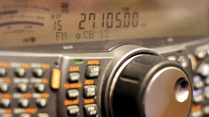
Phase-locked Loop is an essential element in digital and analog frequency modulation systems
Key Takeaways
A phase-locked loop (PLL) is a negative feedback loop that forces a voltage-controlled oscillator to match the phase and frequency of a reference signal, using a phase detector, a loop filter, and a frequency divider.[1]
Loop dynamics depend on two factors, i.e., natural frequency (ωn) and damping factor (ζ).[2]
Type-II charge-pump PLLs dominate modern integrated circuits because they give zero static phase error and decouple the stability-versus-ripple trade-off that limits type-I loops.[3]
The choice of a phase detector depends on lock range, capture range, and noise tolerance. A phase/frequency detector (PFD) makes lock range equal to capture range and independent of the low-pass filter.[4]
Wider bandwidth in PLLs leads to faster tracking and lower in-band phase noise.[5]
PLLs allow frequency multiplication by N, making them a preferred option for network analyzer signal sources.[6]
Introduction
A phase-locked loop is a negative feedback control system that drives the phase difference between a reference signal and a locally generated signal toward a constant value.[1] When that phase difference stops changing, the two signals are at the same frequency. This is a defining property, as phase lock ensures exact frequency equality, not merely a close match.
Thanks to this property, PLLs are everywhere. They generate the multi-gigahertz clocks inside processors from a cheap crystal, recover timing from a serial data stream that carries no separate clock, demodulate frequency-modulated signals, and synthesize the local oscillator in every radio transceiver.
The concept dates to the 1930s and became practical in the 1950s and 1960s in radio modulation and demodulation, before integrated circuits made it ubiquitous in telecommunications and digital signal processing.[5]
This article discusses the basic loop, through the design equations you need to size a loop filter, then into phase noise, synthesis architectures, and the mistakes that cost the most debugging time.
What Is a Phase-Locked Loop?
A PLL is a negative-feedback system in which an oscillator-generated signal is phase- and frequency-locked to a reference signal.[1]
The loop compares the phase of its own output against the input signal, produces an error signal proportional to the difference, filters it, and uses the result to steer its oscillator. If the oscillator runs fast, the error signal pushes it slower. If it runs slow, the error signal pushes it faster.
Think of a phase-locked loop as a feedback control system in the phase domain rather than the voltage domain. The transfer function of an ordinary amplifier indicates how an input voltage propagates to the output.[2] The transfer function of a PLL tells you how a slow or fast change in the input excess phase propagates to the output.
The loop is said to be locked when the difference between output phase and input phase is constant with time. An important and unique consequence is that the input and output frequencies of the PLL are then exactly equal.
The Four Building Blocks of a PLL
Every PLL, from a 1970s CMOS integrated circuit to a modern all-digital design, is assembled from the same four functional blocks.
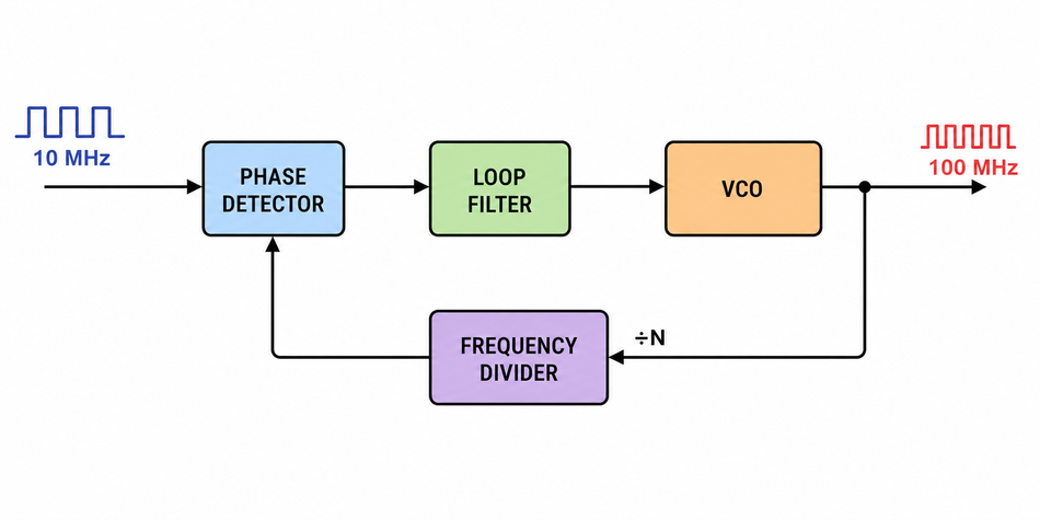
1. Phase Detector
The phase detector senses two periodic inputs and produces an output whose average value is proportional to the difference between their phases.[5] The slope of that input/output characteristic is the phase detector gain, KPD, expressed in volts per radian.
Because the loop filter averages the detector output, you characterize KPD from the average output voltage or current, not the instantaneous pulse waveform.
2. Loop Filter
The loop filter is a low-pass filter that extracts the average of the phase detector error pulses and smooths them into a clean control voltage.
It exists for two reasons:
It produces repetitive pulses that would otherwise modulate the oscillator frequency and generating large sidebands.[5]
Sets the loop bandwidth, which determines how fast the loop locks and how stable it is once locked.[5]
A first-order RC filter with a series resistor gives you a proportional term and an integral term. That makes the loop filter functionally a PI stage, the same structure as a PID controller without the derivative branch.
3. Voltage-Controlled Oscillator (VCO)
The voltage-controlled oscillator converts the control voltage into an output frequency.[2] Its gain, KVCO, is expressed in radians per second per volt, or more conveniently in MHz/V.
The key modeling insight is that the VCO is an integrator in the phase domain. Frequency is the derivative of phase, so if the VCO sets frequency proportionally to control voltage, its phase is the integral of that voltage. In the Laplace domain, the VCO contributes KVCO/s.[3]
4. Frequency Divider
Insert a divide-by-N counter in the feedback path, and the loop must run its VCO at N times the reference frequency to satisfy the phase comparison.[6] That is frequency synthesis: a 50 MHz crystal reference and N = 64 gives you a 3.2 GHz output.
The divider is not free. It divides the KVCO by N in the loop gain, which makes the loop less stable and requires larger charge-pump current or loop capacitance to compensate. It also multiplies the static phase error by N.
Phase Detector Types Compared
The phase detector you pick determines the loop's acquisition behavior more than any other single choice. The typical CMOS 4046 family is a good reference because it exposes three different comparators on the same die.[4]
Property | PC1 (XOR gate) | PC2 (PFD) | PC3 (RS flip-flop) |
Type | Analog-like multiplier or XOR | Edge-triggered phase and frequency detector | |
Phase at center frequency | 90° | 0° | 180° |
Phase range | 0 to π rad | -2π to +2π rad | 0 to 2π rad |
Input duty cycle sensitive | Yes | No | No |
Lock range vs capture range | Capture depends on loop filter, can approach lock range | Lock range equals capture range, independent of filter | Both depend on loop filter |
Locks to harmonics | Yes | No | No |
Noisy-input tolerance | High, stays locked with very noisy inputs | Lower | Lower |
Output ripple | Moderate | Lowest (3-state when locked) | Highest, larger voltage swing |
Static phase error | 90° offset | Zero | 180° offset |
Three practical consequences follow.
If the input signal is noisy or buried in interference, PC1-style XOR detection is the robust choice, because it keeps averaging through dropouts. Its penalty is a permanent 90° phase offset and the ability to false-lock onto harmonics of the VCO center frequency.[4]
If you need guaranteed acquisition over the full VCO range, use a PFD. At the start of a transient, it behaves as a frequency detector, pushing the VCO frequency toward the input frequency; once the two are close, it reverts to phase detection and pulls the loop into phase lock.[4]
The PFD also gives you a free lock indicator. In the 74HC4046A, when the loop is locked, the PC2 output goes to a high-impedance state, and the phase comparator pulse output sits at a HIGH level, which you can sample directly as a lock flag.[4]
Type-I vs Type-II PLLs
"Type" counts poles at the origin in the open-loop transfer function. "Order" counts total poles. The distinction matters more than the naming suggests.
A type-I PLL has one pole at the origin, contributed by the VCO. Its loop filter is a passive low-pass with no integrator.[3]
Type-I loops have three well-documented drawbacks[3]:
A tight coupling between stability and ripple. Ripple on the control line modulates the VCO and must be suppressed by lowering the filter corner frequency, but lowering it degrades stability. You cannot optimize both.
Limited acquisition range. If the VCO frequency and input frequency are far apart at start-up, the loop may never acquire lock at all.
Finite static phase error that varies with frequency. A frequency change of Δω requires the control voltage to change by Δω/KVCO, which forces a proportional change in phase error. Minimizing this variation means maximizing the KPD·KVCO product, often loosely called the loop gain.
A type-II PLL adds a second pole at the origin, almost always by replacing the passive filter with a charge pump feeding a capacitor. The charge pump has infinite DC gain. An arbitrarily small constant phase difference still turns a switch on and drives the control voltage toward its rail until the error is nulled.[3]
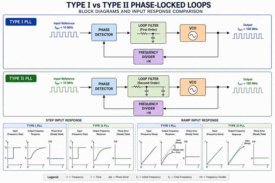
Two cascaded integrators are unconditionally unstable, so you stabilize the loop by inserting a resistor in series with the capacitor, creating a lossy integrator. That circuit is the charge-pump PLL (CPPLL), and it is the default topology in modern integrated circuits.
In a charge-pump PLL, increasing C₁ increases the damping factor, the opposite of the type-I trend. Eventually, it removes the trade-off between stability and ripple amplitude.
Suggested Reading: Active Filters: Types, Circuit Design, and How They Compare to Passive Filters
Natural Frequency and Damping Factor
Once locked (or near lock, with small phase deviations), a PLL is well described by a linear second-order model. Write the closed-loop denominator in the standard prototype form:
s² + 2ζωn·s + ωn²
where ωn is the natural undamped frequency and ζ is the damping factor. These two parameters determine the transient response.[2]
The design equations that follow from this form are:
Parameter | Expression | Design meaning |
Damped frequency | ω = ωn·√(1 - ζ²) | Ringing frequency of the transient |
Damping factor (real part) | α = ζωn | Envelope decay rate |
Settling time | ts ≈ 4/(ζωn) | Time to settle within tolerance |
Peak overshoot time | tmax = π/(ωn√(1 - ζ²)) | When the worst overshoot occurs |
Maximum overshoot | M = 1 + e^(-ζπ/√(1-ζ²)) | Peak excursion after a step |
Loop time constant | between 1/(ζωn) and 1/(2ζωn) | Rule-of-thumb lock time scale |
For a charge-pump PLL, the closed-loop response also contains a zero at
ωz = -ωn/(2ζ) = -1/(R₁C₁)
This zero makes the loop stable, and it is why you cannot analyze a type-II PLL as a textbook two-pole system.[3]
Setting the Damping Factor
The damping factor is the number most designs get wrong first.
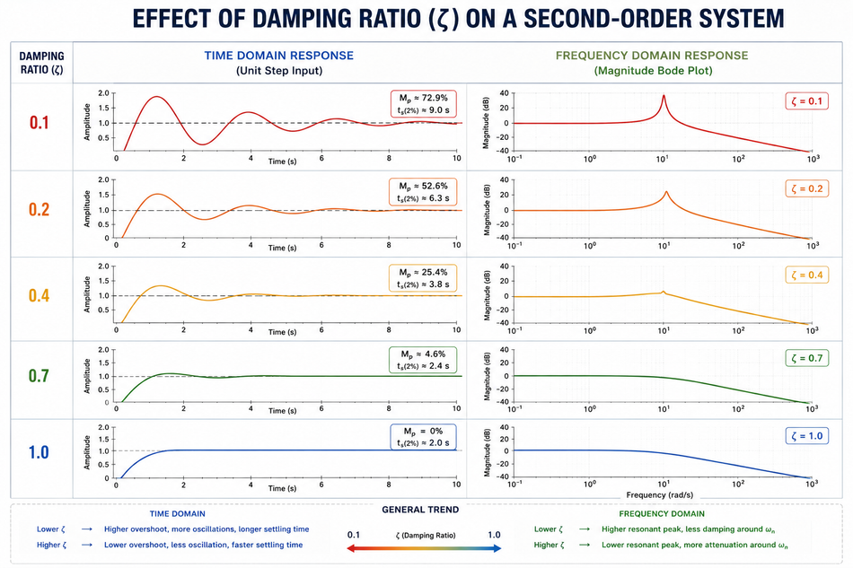
If ζ is too low, the closed-loop response peaks in the frequency domain, which appears as ringing in the time domain. Set ζ = 0.1, and a frequency step produces a badly underdamped response. At ζ = 0.707 to 1, the response settles cleanly.[3]
Counterintuitively, excessively high damping also causes peaking, though you need a third-order model to see it. Damping around 1 is usually preferred.
In practice, typical designs choose ζ = 0.8 to 1.
Sizing the Second Capacitor
A single R₁C₁ loop filter does not suppress ripple sufficiently even in the locked condition. The ripple consists of positive and negative pulses of amplitude Ip·R₁ occurring every reference period.
The standard fix is a second capacitor C₂ tied from the control line directly to ground. More C₂ means less ripple, but it introduces a higher-frequency pole that degrades phase margin:
C₂ relative to C₁ | Phase margin at ζ = 1 |
C₂ much smaller than C₁ | 76° |
C₂ ≈ 0.2·C₁ | 42° |
Typical designs settle on C₂ ≈ 0.2·C₁ with ζ = 0.8 to 1, accepting roughly 42° of phase margin in exchange for adequate ripple suppression.
A representative worked parameter set from a teaching example: KPD = 25 µA/2π, KVCO = 2π·40 MHz/V, and N = 32, with damping swept from 0.1 to 2 to show the response family.
Lock Range vs Capture Range
These two ranges are routinely confused, and the distinction has real design consequences.
Frequency lock range (2fL) is the range of input frequencies over which a loop that is already locked will stay locked.[4]
Frequency capture range (2fc) is the range of input frequencies over which a loop that is initially out of lock will acquire lock.[4]
The capture range is always smaller than or equal to the lock range.
The gap between them is a startup hazard. A loop can hold the lock perfectly across a wide band during bench testing, then fail to acquire that same frequency after a power cycle. If you have ever had a design that "works until you reset it," this asymmetry is the first thing to check.
With an XOR-type comparator, the capture range depends on the low-pass filter characteristics and can be made as large as the lock range with careful filter design. With a PFD, the lock range simply equals the capture range and is independent of the low-pass filter, which is the cleanest solution and another reason PFDs dominate.
Recommended Reading: What Is a Low Pass Filter? Theory, Design & Practical Implementation
Phase Noise and Jitter in PLLs
Phase noise is the frequency-domain description of the same imperfection that jitter describes in the time domain. Single-sideband phase noise L(f) is expressed in dBc/Hz at a specified offset from the carrier.
The 20·log(N) penalty
This is the most important single relationship in synthesizer design.
A PLL performing frequency multiplication amplifies low-frequency reference phase noise proportionally to the multiplication factor. In-band phase noise rises by 20·log(N) dB.
The magnitude is startling. If your crystal reference has a phase noise of -150 dBc/Hz and you multiply by M = 2400, then 20·log(2400) = 68 dB, so the output phase noise within the loop bandwidth degrades to -82 dBc/Hz.[3]
The practical lesson: a low N is worth more than a good VCO for in-band noise. Doubling your reference frequency and halving N buys you 6 dB.
Loop Bandwidth Shapes the Noise
The loop applies opposite filtering to its two dominant noise sources:
Noise source | Shaping by the loop | Implication |
VCO phase noise | The loop suppresses slow VCO variations but cannot correct fast ones. Wider loop bandwidth suppresses more VCO noise. | |
Reference and divider noise | Low-pass | Passed through and multiplied by 20·log(N) inside the loop bandwidth. Wider loop bandwidth passes more of it. |
Optimum loop bandwidth sits at the crossover where the multiplied reference noise floor meets the VCO noise curve.[3] Crystal oscillators typically display a flat phase noise profile beyond an offset of a few kilohertz, which usually puts that crossover in the tens to hundreds of kilohertz for RF synthesizers.
There is a second, subtler effect of the divider. A loop with a divide ratio N makes phase comparisons N times less often than a divider-less loop at the same output frequency, so the VCO accumulates phase noise for N cycles before receiving any correction.
Suggested Reading: Crystal Oscillator Circuit Design: Pierce Oscillator Guide for Precision Frequency Generation
Integer-N vs Fractional-N Frequency Synthesis
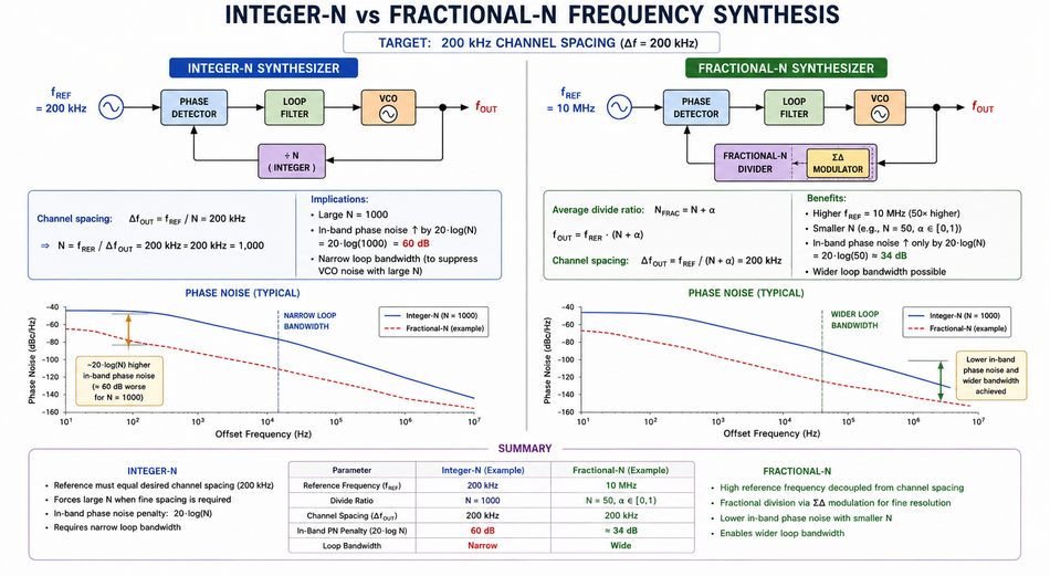
An integer-N synthesizer divides by a whole number, so its output frequency resolution equals the reference frequency at the phase detector.[5] For instance, if you want 200 kHz channel spacing, then your reference must be 200 kHz. Eventually, it will force N to be large, driving in-band phase noise by 20·log(N) and forcing a narrow loop bandwidth.
A fractional-N synthesizer breaks that coupling by dithering the divider between adjacent integer values so the average divide ratio is fractional. It uses advanced algorithms like Sigma-Delta modulation to achieve fine frequency resolution and a high phase detector frequency at the same time, which permits both a lower N and a wider loop bandwidth.[5]
Aspect | Integer-N | Fractional-N |
Frequency resolution | Equal to phase detector frequency | Far finer than reference |
In-band phase noise | Higher (large N) | Lower (small N) |
Loop bandwidth | Constrained narrow | Can be wide |
Dominant spur problem | Reference spurs at the reference frequency | Fractional spurs |
Complexity | Low | Requires delta-sigma modulator |
The cost is fractional spurs, created by the periodic pattern of the divider modulation. Delta-sigma modulation shapes that quantization noise to high frequencies where the loop filter attenuates it.
Even so, published designs still report fractional spurs around -59 dBc, with performance often capped near -63.7 dBc by natural DAC matching.[5]
PLL Applications
The same loop serves very different purposes depending on which node you treat as the output.
Frequency synthesis and clock generation: Multiply a stable low-frequency reference clock up to a high output frequency, for example, a 100 MHz reference to a 10 GHz carrier. This is the dominant use in RF and processor design.[1]
Clock recovery and signal recovery: Extract the clock frequency and optimum sampling phase from an incoming serial data stream that carries no separate clock. Essential in every high-speed link.[1]
Skew cancellation: Phase-align an internal clock to an external I/O clock, canceling distribution delay.[1]
FM and FSK demodulation: Take the control voltage as the output instead of the VCO signal. If the input frequency toggles between two values, the control voltage must toggle to track it, reproducing the original bit stream.[1]
Signal sources and instrumentation: In network analyzers, a PLL generates a high-frequency source from a stable low-frequency reference, and sweeping the divisor N sweeps the output frequency.[6]
Suggested Reading: Instrumentation Amplifier: Theory, Three-Op-Amp Design, CMRR
Common Design Mistakes and Troubleshooting
Picking the Wrong Model
Analyzing a charge-pump PLL as a plain two-pole system ignores the stabilizing zero and gives a nonsense answer. Always include the zero at 1/(R₁C₁), and include C₂ when checking phase margin.
Ignoring Loop Gain Division
The frequency divider will reduce the loop gain. Therefore, adding a divide-by-N reduces effective KVCO by N and makes the loop less stable. If you raise N without raising charge-pump current Ip or C₁, a loop that was well damped becomes underdamped.
Chasing Ripple Until the LoopRings
Every increase in C₂ buys ripple suppression and costs phase margin. Going from a very small C₂ to C₂ ≈ 0.2·C₁ takes you from 76° to 42° of phase margin. Past that, you are trading stability for a diminishing ripple return.
Assuming Lock Range Equals Capture Range
True for a PFD, not for XOR or RS-flip-flop detectors. Test acquisition from a cold start across the full input frequency range, not just steady-state hold.
False Lock on Harmonics
An XOR phase detector can lock to input frequencies close to the harmonics of the VCO center frequency. If your loop locks but the output is at the wrong multiple, this is usually why.
For bench debugging, probe the VCO control voltage with an oscilloscope. A clean settled DC level means lock. Periodic ripple at the reference rate points to charge-pump mismatch or insufficient filtering. A slow ramp or a sawtooth means the loop never acquired and is beating against the input.
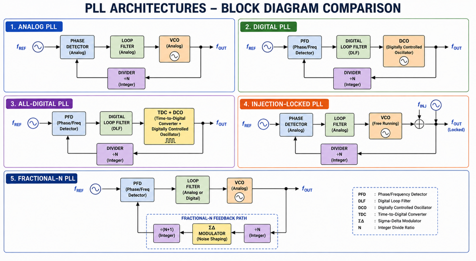
PLL Architectures and Where the Field Is Heading
Modern PLL design spans several architectures, and no single one wins on every metric.
Analog PLLs (APLLs) deliver low-jitter performance for high-frequency analog systems.[2]
Digital and all-digital PLLs (ADPLLs) replace the charge pump with a time-to-digital converter and the analog filter with digital logic. They gain programmability, small area, and insensitivity to process, voltage, and temperature variation, and they scale well into deep-submicron CMOS where analog circuits suffer from reduced supply voltage.[2]
Fractional-N PLLs with delta-sigma modulation give fine resolution and wide bandwidth.
Injection-locked PLLs target very low jitter and fast locking.
The decade from 2016 to 2025 produced measurable progress across the board:
Metric | Trend (2016 to 2025) |
Integrated jitter | Improved about 2.5 times per decade, from 0.16 ps RMS to 65 fs RMS |
Jitter figure of merit | Improved 8.5 dB per decade, reaching -272 dB in a 2025 design |
Output bandwidth | Expanded roughly 10 times per decade, from 2.4 GHz to a 9.05 to 37.0 GHz range[3] |
Low-power designs | Down to 380 µW for IoT, using duty-cycled architectures |
Silicon area | Below 0.05 mm² in 14 nm and 22 nm nodes |
Designs are compared using a jitter-power figure of merit, where lower is better.
FOM = 10·log₁₀ of [(Jitter in seconds)² × (Power in mW)]
Looking forward, ADPLLs are expected to dominate low-power Wi-Fi, Bluetooth, and IoT applications, while digital-to-time-converter calibration, adaptive bandwidth control, and machine-learning-assisted optimization are the active research fronts.
Conclusion
A phase-locked loop is conceptually simple and practically demanding. The concept is a negative feedback loop that nulls phase error; the difficulty is that the two parameters governing its behavior, natural frequency and damping factor, are set indirectly by component values that also control ripple, lock time, and noise.
If you take three things into your next design: target a damping factor of 0.8 to 1 with C₂ around 0.2·C₁, use a PFD unless you specifically need XOR noise immunity, and remember that every factor of N in your divider costs 20·log(N) dB of in-band phase noise.
Frequently Asked Questions
1. What is a phase-locked loop in simple terms?
It is a circuit that makes one oscillator follow another. It continuously measures the phase difference between an incoming reference signal and its own output, then adjusts its own oscillator to drive that difference to a constant. When the phase difference stops changing, the two signals are at the same frequency.
2. What are the three main components of a PLL?
A phase detector, a loop filter (a low-pass filter), and a voltage-controlled oscillator. A fourth block, a frequency divider in the feedback path, is added whenever you want the output frequency to be a multiple of the reference.
3. Why does a PLL use a low-pass filter?
The phase detector produces repetitive pulses rather than a smooth voltage. Without filtering, those pulses would modulate the VCO and create large sidebands. The filter extracts the average, and in doing so, it also sets the loop bandwidth and stability.
4. What damping factor should I design for?
Between 0.8 and 1 for most applications. Below about 0.5 you get frequency-domain peaking and time-domain ringing. Excessively high damping also causes peaking in a third-order model.
5. How does a PLL demodulate an FM signal?
Take the loop filter output (the VCO control voltage) as your signal rather than the VCO output. Since the control voltage must track the input frequency for the loop to stay locked, it directly reproduces the modulating waveform. The same mechanism recovers the bit stream from an FSK signal.
6. Is a PLL the same as a PID controller?
Not the same, but closely related. A PLL is a feedback control system whose controlled variable is phase, and its loop filter typically implements proportional and integral action, like a PID controller without the derivative term. The VCO adds a further integration, which is why loop stability requires careful compensation.
7. What causes reference spurs in a PLL?
Ripple on the VCO control line at the reference rate. The main sources are charge-pump up and down current mismatch, charge injection and clock feedthrough from the switches, and insufficient loop filtering.
References
Palermo, S. Lecture 26: Phase-Locked Loops. ECEN 689, Analog and Mixed-Signal Center, Texas A&M University. https://people.engr.tamu.edu/spalermo/ecen689/lecture26_ee689_pll.pdf
Texas Instruments. Introduction to phase-locked loop system modeling, Analog Applications Journal, SLYT169. https://www.ti.com/lit/pdf/slyt169
Razavi, B. Design of CMOS Phase-Locked Loops, Chapter 9: Phase-Locked Loops. National Taiwan University course notes. https://cc.ee.ntu.edu.tw/~ecl/Courses/111PLL/lock/PLL_Ch9.pdf
Nexperia. 74HC4046A; 74HCT4046A Phase-locked loop with VCO, Product data sheet Rev. 7, 7 May 2024. https://assets.nexperia.com/documents/data-sheet/74HC_HCT4046A.pdf
Nguyen, T.V.H. and Pham, C.-K. An Overview of Phase-Locked Loop: From Fundamentals to the Frontier. Sensors 2025, 25(18), 5623. https://www.mdpi.com/1424-8220/25/18/5623
Keysight Technologies. Consider the Source Part 1: What is a Phase-Locked Loop? https://www.keysight.com/blogs/en/tech/rfmw/2020/12/08/consider-the-source-part-1-what-is-a-phase-locked-loop
in this article
1. Introduction2. What Is a Phase-Locked Loop?3. The Four Building Blocks of a PLL4. Phase Detector Types Compared5. Type-I vs Type-II PLLs6. Natural Frequency and Damping Factor7. Lock Range vs Capture Range8. Phase Noise and Jitter in PLLs9. Integer-N vs Fractional-N Frequency Synthesis10. PLL Applications11. Common Design Mistakes and Troubleshooting12. PLL Architectures and Where the Field Is Heading13. Conclusion14. Frequently Asked Questions15. References