Signal Integrity Testing for High-Speed PCB Design
How engineers measure jitter, crosstalk, impedance, eye margin, and BER for reliable PCB designs

01 Aug, 2026. 17 minutes read
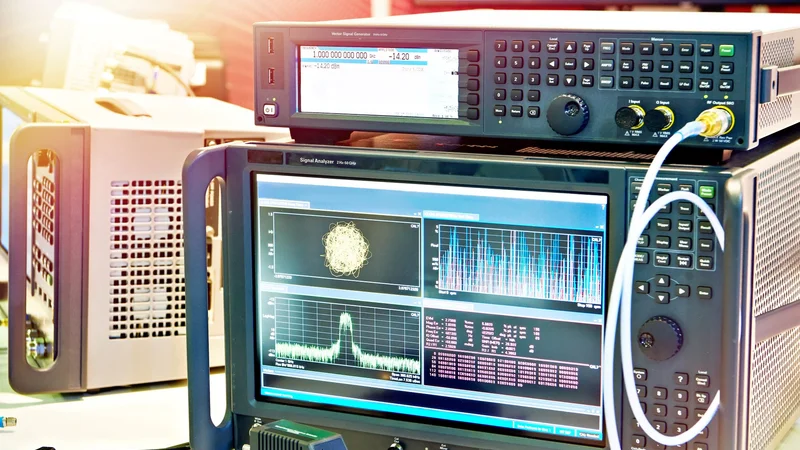
A spectrum analyzer and signal generator are two of the fundamental equipment used in signal integrity testing
Key Takeaways
Signal integrity testing verifies that PCB interconnects preserve timing, voltage, impedance, and noise margins under real operating conditions.[1]
The oscilloscope is the primary time-domain instrument for waveform capture, eye diagram analysis, jitter measurement, and compliance mask testing.
TDR and TDT locate impedance discontinuities in vias, connectors, packages, cables, and transmission line structures.[2]
A vector network analyzer measures S-parameters such as insertion loss, return loss, mode conversion, and coupling across the frequency range.[3]
BERT measurements validate link robustness by measuring the bit error rate, often at thresholds such as 1e-12 or lower, depending on the interface and compliance requirements.
Practical signal integrity testing depends as much on fixtures, probing, calibration, and de-embedding as it does on the DUT itself.
Introduction
Signal integrity is the discipline of studying pulse distortion. The study ensures that a high-speed digital signal launched by a transmitter arrives at the receiver with enough amplitude, timing margin, and waveform quality to be decoded correctly[1]. At low edge rates, a PCB trace can often be treated as a simple connection. At modern edge rates, the same trace behaves as a transmission line with controlled impedance, propagation delay, frequency-dependent loss, coupling to neighboring conductors, and sensitivity to return-current discontinuities.
Signal integrity testing is the measurement-driven part of that discipline. It tells whether the real PCB behaves like the design, simulation, and compliance plan, and depends on multiple failure mechanisms:
Reflections and ringing from impedance mismatch
Crosstalk between adjacent routes
Jitter from clocks and data-dependent effects
Attenuation and dispersion in lossy dielectric and copper
Skew between related signals
Intersymbol interference
Power integrity noise and EMI.
The core instruments for signal integrity testing are the high-bandwidth oscilloscope and digital signal analyzers. But as signal speeds increased to gigabits, TDR, vector network analyzer, BERT[1], and spectrum analyzers have become more relevant. Each of these methods sees the channel from a different perspective. For instance:
A scope shows voltage versus time and builds the eye diagram.
TDR shows impedance and quality of signal paths.[2]
A VNA shows S-parameters versus frequency.
A BERT measures whether a real receiver path can carry bits at the required error rate.
A spectrum analyzer helps identify emissions, spurs, phase noise, and coupling mechanisms that may not be obvious in the time domain.
This article is a practical engineering reference for high-speed digital, PCB layout, validation, and test engineers. It focuses on what fails, how to measure it, how to interpret the results, and how to build a workflow that correlates simulation, bench measurement, and compliance requirements.
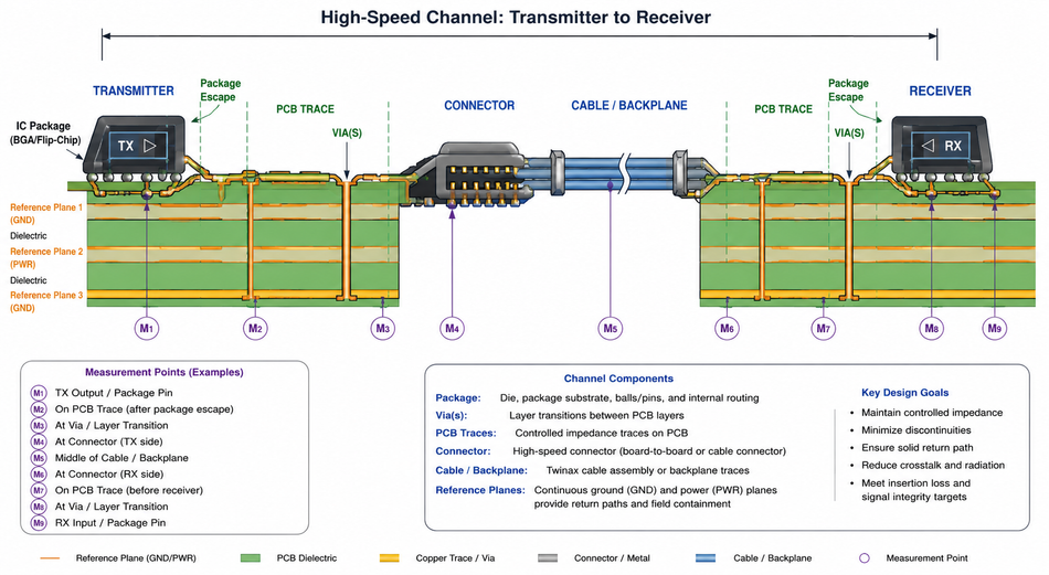
Validation with Signal Integrity Testing
A high-speed digital channel is more than just a copper path. It is an electromagnetic structure that includes the transmitter package, breakout vias, PCB transmission line, reference planes, connectors, cables, AC coupling capacitors, receiver package, termination, and the return-current path. Signal integrity testing verifies that this complete interconnect preserves enough margin at the receiver sampling point.
The basic pass condition is that the receiver must reliably distinguish logic states at the correct sampling time. But in reality, the waveform can be degraded by loss, reflection, noise, jitter, and interference.
Usually, engineers target a 50-ohm impedance for single-ended structures in RF, coaxial, lab, and controlled-impedance measurement systems, and 100 ohm differential structures in high-speed differential interconnects.
Signal integrity testing usually validates four classes of behavior:
Validation area | What is measured | Why it matters |
Voltage margin | Eye height, overshoot, undershoot, noise, mask hits | Determines whether the receiver can resolve logic levels |
Timing margin | Eye width, jitter, skew, setup and hold margin | Determines whether sampling occurs in the valid data window |
Channel quality | Impedance, S-parameters, insertion loss, return loss, crosstalk | Determines whether the interconnect preserves signal energy |
Link reliability | Bit error rate, link margin, equalizer setting, receiver tolerance | Determines whether the system works over time and variation |
For a parallel bus, signal integrity often centers on timing skew, simultaneous switching noise, ringing, overshoot, undershoot, and setup or hold margin.
For a SerDes channel, the emphasis shifts toward eye diagram margin, insertion loss, return loss, mode conversion, jitter tolerance, equalization, and BER.
Suggested Reading: Signal Integrity in High Speed Digital Systems: Theory & Practice
Failure Mechanisms in High-Speed PCB Interconnects
Impedance Mismatch and Reflections
A reflection occurs when a traveling wave encounters a change in impedance. The discontinuity arises due to many reasons, like an unterminated trace, connector transition, via stub, test pad, package escape, poor return path, abrupt trace width change, or capacitive load.
Due to the discontinuity, the reflected energy travels back through the channel and can create ringing, overshoot, undershoot, double-clocking, or eye closure.
The reflection coefficient is:
rho = (ZL - Z0) / (ZL + Z0)
where Z0 is the source transmission line impedance, and ZL is the impedance seen at the discontinuity.
A positive reflection indicates a higher impedance discontinuity
A negative reflection indicates a lower impedance discontinuity.
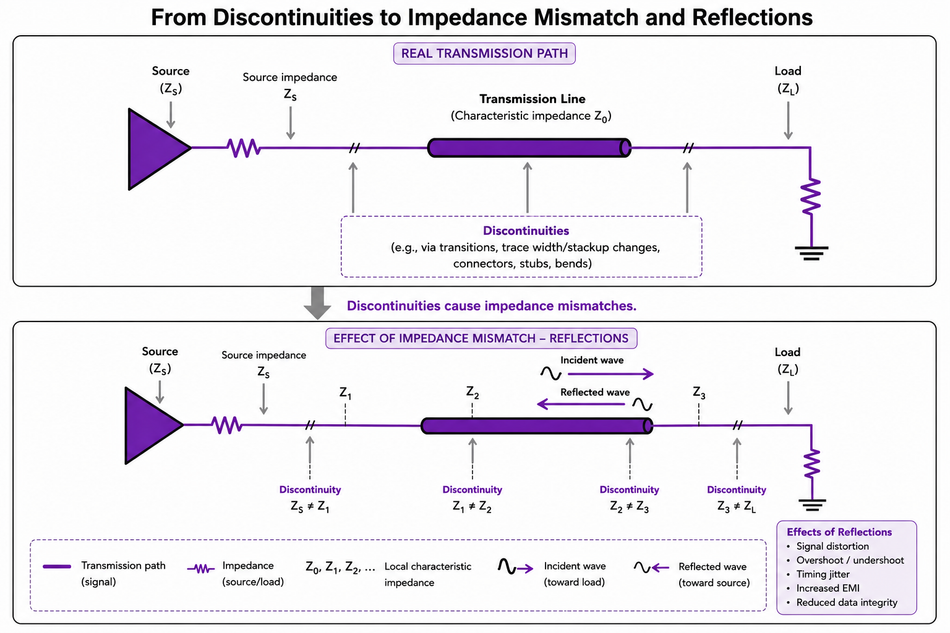
Impedance matching is therefore critical, as it ensures there is no signal reflection.[4] But it does not mean every structure is exactly 50 ohm or exactly 100 ohm differential. It means the channel impedance is controlled tightly enough that reflections do not consume the allowed timing and voltage margin for the target interface.
Crosstalk Between Traces and Planes
Crosstalk occurs when energy from an aggressor signal couples into a victim signal through mutual capacitance, mutual inductance, or shared return paths. It generally happens when high-speed routes are close together, run in parallel for long distances, cross splits in ground planes, or share vias and reference transitions without adequate return-current control.
Near-end crosstalk appears at the transmitter side of the victim. Differential pairs reject some common-mode noise, but poor pair symmetry, skew[1], return path discontinuity, and mode conversion can turn differential energy into common-mode energy and increase EMI.
Suggested Reading: Why is Picking the Right Trace Width Important?
Jitter and Skew
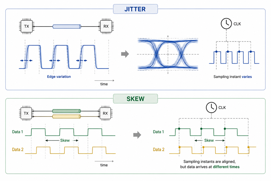
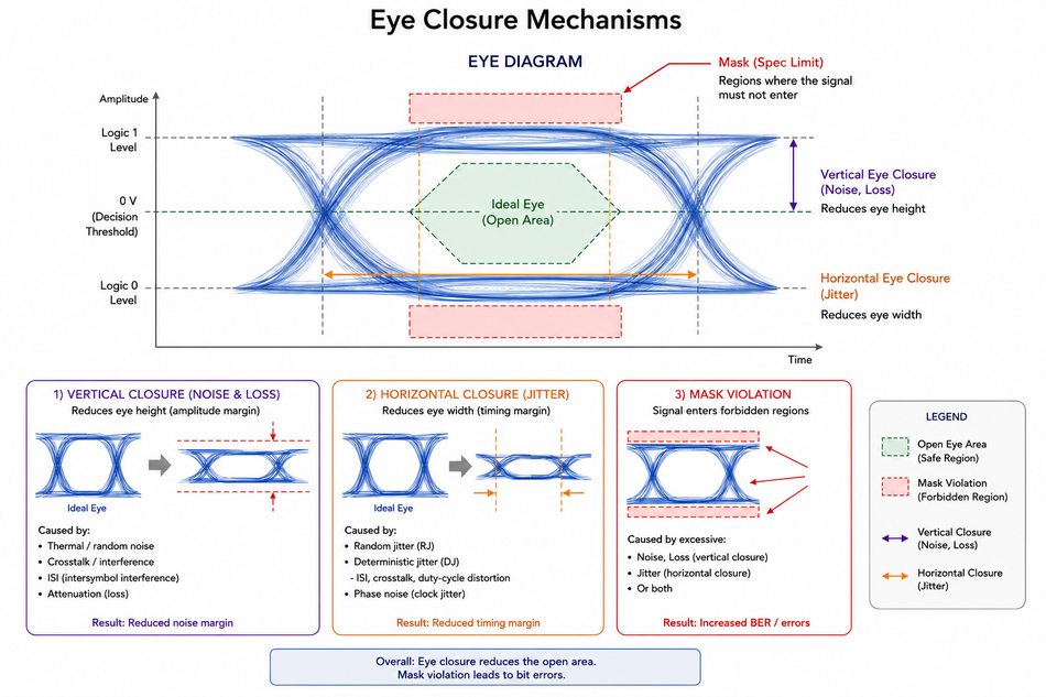
Jitter is the deviation of a signal transition from its ideal time. It reduces horizontal eye opening and can directly violate setup and hold timing. Jitter is usually created through thermal noise, crosstalk, and noisy ground connections.[1]
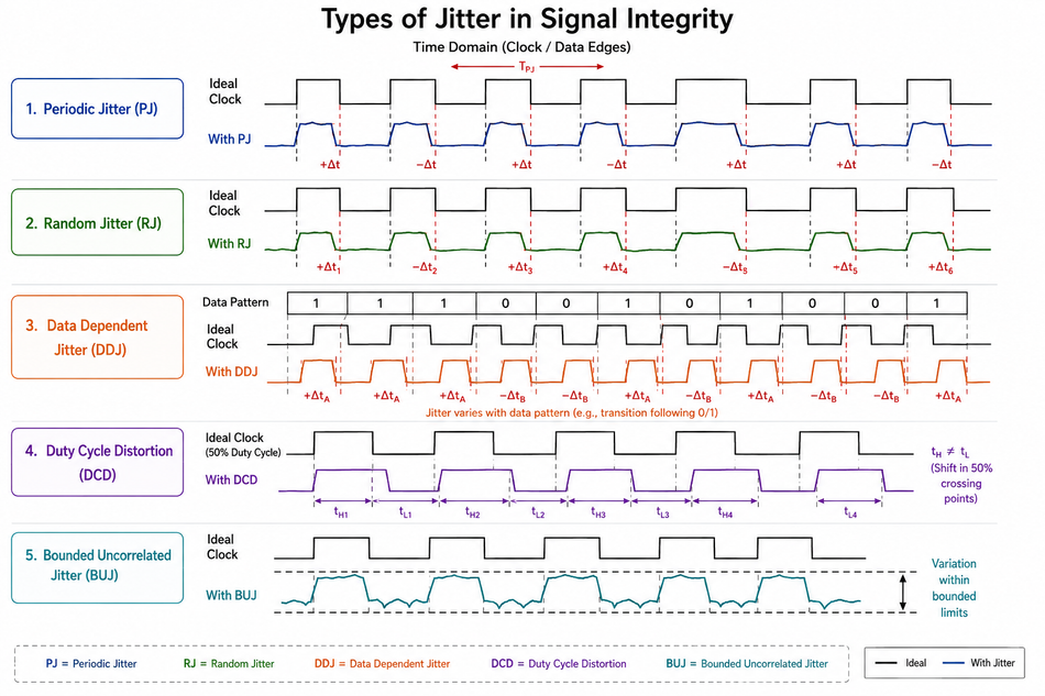
Engineers commonly decompose jitter into random jitter and deterministic jitter.
Random jitter is usually treated as unbounded and often associated with thermal noise, oscillator phase noise, and other stochastic mechanisms.
Deterministic jitter is bounded and includes data-dependent jitter, duty-cycle distortion, periodic jitter, and crosstalk-induced components.
Modern oscilloscope jitter tools commonly combine eye diagram analysis, mask testing, histograms, bathtub curves, and jitter decomposition.
Skew is a relative timing error between two or more signals. In differential routing, intra-pair skew converts differential energy into common-mode energy and closes the eye. In a DDR byte lane or other parallel bus, inter-signal skew reduces setup and hold margin at the sampling latch.
Attenuation and Dispersion
Attenuation reduces the high-frequency content of a signal as it propagates through copper and dielectric material. The major contributors to attenuation are skin effect, dielectric loss, surface roughness, and package or connector loss all contribute.
On the other hand, dispersion occurs when different frequency components travel with different phase delay or group delay. It results in pulse spreading.
In digital channels, pulse spreading causes Inter-Symbol Interference (ISI). A bit is no longer affected only by the current transmitted symbol. Instead, it is affected by previous symbols. ISI reduces eye height and eye width, adds deterministic jitter, and increases the burden on equalization.[1]
Power Integrity and EMI Coupling
Power integrity is closely related to signal integrity because the transmitter, receiver, Phase Locked Loop (PLL), clock tree, and termination network all depend on low-noise power distribution. Supply ripple can modulate threshold voltages, introduce deterministic jitter, and degrade phase noise.
Electromagnetic Interference (EMI) is both a symptom and a failure mode. Even though the differential data may appear to be working properly, asymmetric differential pairs can cause common-mode currents. Likewise, plane breaks, connector transitions, and mode conversions tend to cause electromagnetic radiation. That’s why a PCB may pass the BER test but can still fail the emissions test.
Further Reading: PCBA Signal Integrity Problems: Ten Factors to Consider
SI Test Instruments and Methods
The right signal integrity test depends on whether the question is time-domain behavior, impedance discontinuity, frequency-domain channel loss, error rate, or emissions. There is no single instrument that deals with all signal integrity testing mechanisms.
Instrument or method | Primary measurement | Detects | Typical engineering use | Watchouts |
High-bandwidth oscilloscope | Waveforms, eye diagram, jitter, mask hits | Overshoot, undershoot, ringing, eye closure, timing errors | Compliance, debug, clock and data validation | Bandwidth, probe loading, clock recovery settings, sample rate |
TDR | Reflected step versus time, impedance profile | Impedance discontinuities, via stubs, connector mismatch, trace width errors | Locate physical defects and stackup mismatch | Rise time limits spatial resolution |
Vector network analyzer | S-parameters versus frequency | Insertion loss, return loss, crosstalk, mode conversion | Channel characterization and model correlation | Calibration, port quality, fixture de-embedding |
BERT | Bit error rate versus stress condition | Link-level reliability failure | SerDes validation, receiver margining | Test time, confidence level, pattern dependence |
Spectrum analyzer | Frequency spectrum, spurs, EMI, phase noise | Emissions, clock spurs, switching noise, coupling paths | EMI debug and clock noise analysis | Near-field scans are diagnostic, not full compliance |
Waveform and Eye Diagram Analysis with Oscilloscopes
A real-time oscilloscope captures voltage versus time. In signal integrity testing, it is used to check edge rate, amplitude, overshoot, undershoot, ringing, duty cycle, timing, and noise. With repetitive data, the scope overlays many unit intervals to build an eye diagram.
An eye diagram compresses thousands or millions of bit transitions into a visual probability map. Eye height indicates vertical noise and amplitude margin. Eye width indicates timing margin. A compliance mask defines forbidden regions in the eye.
During mask testing, the instrument accumulates samples and reports whether the signal violates the mask under the specified test conditions. The mask is only meaningful when the correct standard, bit rate, test point, fixture, termination, pattern, and clock recovery method are used.[5]
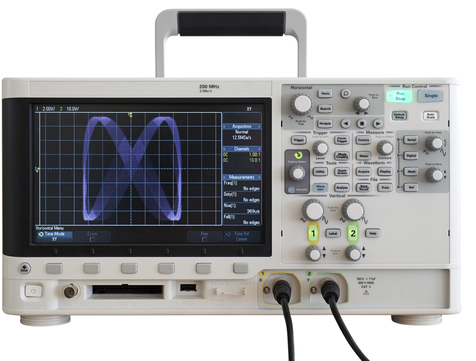
Jitter analysis extends the eye diagram by quantifying transition timing error.[5] Measurements such as time interval error, histograms, etc., help separate random mechanisms from deterministic mechanisms. This distinction matters because total jitter is usually estimated at a target BER, not simply measured as peak-to-peak jitter from a short capture.[5]
Probe selection is a critical aspect. A passive probe that is acceptable for low-speed debug can severely load a high-speed node. Often, differential active probes, solder-in tips, coaxial launches, or compliance fixtures are required.
Moreover, the measurement bandwidth should include the signal content needed for the edge rate and standard under test. Too little bandwidth hides overshoot and jitter, while too much bandwidth without proper noise control can reduce apparent margin.
Impedance Measurement with Time Domain Reflectometry (TDR)
Time-domain reflectometry launches a fast edge into the DUT and measures the reflected response. It is one of the most intuitive methods for finding impedance discontinuities in PCB interconnects. It’s similar to using a step generator and oscilloscope to launch a fast pulse edge into the DUT and derive the impedance profile from reflections.[2]
For reflected measurements, the apparent distance to a discontinuity is:
distance = propagation_velocity x reflection_time / 2
The division by two is used because the pulse travels to the discontinuity and the reflection travels back. Additionally, the propagation velocity depends on the effective dielectric constant of the structure.
TDR is especially useful for locating via stubs, connector launch problems, impedance changes caused by stackup variation, trace width errors, poor reference plane transitions, and impedance mismatch at AC coupling capacitors or packages. Differential TDR can measure differential impedance and common-mode behavior.
TDR does not replace VNA measurement. It gives excellent spatial intuition, but its resolution depends on edge speed, fixture quality, and signal-to-noise ratio. Also, the use of cables and connectors contributes to reflection.[2]
Vector Network Analyzers for Evaluating S-Parameters, Insertion Loss, and Return Loss
A vector network analyzer measures the complex ratio of incident, reflected, and transmitted waves. They are typically used in RF and high-frequency applications.[3] The result is a set of S-parameters, including magnitude and phase.
For a two-port single-ended network, common terms include S11 for input reflection, S21 for forward transmission, S12 for reverse transmission, and S22 for output reflection. Rohde & Schwarz describes VNA-based S-parameter measurement as the basis for return loss and insertion loss uncertainty analysis.[6]
For differential high-speed channels, engineers often use mixed-mode S-parameters:
Mixed-mode parameter | Meaning |
Sdd21 | Differential insertion loss |
Sdd11 | Differential return loss at port 1 |
Sdd22 | Differential return loss at port 2 |
Sdc21 | Differential-to-common mode conversion |
Scc21 | Common-mode transmission |
NEXT and FEXT terms | Near-end and far-end coupling between channels |
A VNA is the preferred instrument for characterizing high-speed channels across frequency. It reveals loss slope, resonances, suck-outs from via stubs, connector discontinuities, return loss peaks, crosstalk coupling, and mode conversion.[6]
To ensure VNA accuracy, it’s critical to calibrate and de-embed the instrument. SOLT, TRL, electronic calibration, port extension, and fixture de-embedding move the measurement reference plane closer to the DUT.[7]
Moreover, IEEE Std 370 fixture characterization and 2x-Thru methods are commonly used in high-speed interconnect measurements; Rohde & Schwarz discusses 2x-Thru fixture measurement and de-embedding in the context of PCIe 5.0 CEM connector test fixtures.[7]
BERT to Analyze Bit Error Rate and Link Margin
A bit error rate tester sends a known pattern through a channel and compares the received bits against the expected pattern. BER is:
BER = number_of_bit_errors / number_of_bits_transmitted
A common engineering target for serial links is 1e-12, meaning one error per trillion bits. Some interfaces require lower error rates, higher confidence levels, or additional stress conditions. A zero-error test does not prove the BER is zero; it establishes a statistical upper bound. With zero observed errors, a common 95 percent confidence approximation is that the upper BER bound is about 3 / N, where N is the number of observed bits. Therefore, demonstrating a 95 percent upper bound near 1e-12 requires roughly 3e12 error-free bits.
BERT testing measures practical outcomes, such as correct arrival of bits.[1] Therefore, it is especially useful for stressed receiver testing, equalizer margining, etc.
EMI, Phase Noise and Spurs Analysis with Spectrum Analyzer
A spectrum analyzer shows signal energy versus frequency. In signal integrity debugging, it is used to identify clock spurs, spread-spectrum modulation behavior, switching regulator noise, resonances, and emissions.
With near-field probes, it helps localize radiating structures such as connectors, cable shields, return path discontinuities, board edges, or common-mode currents on differential pairs.
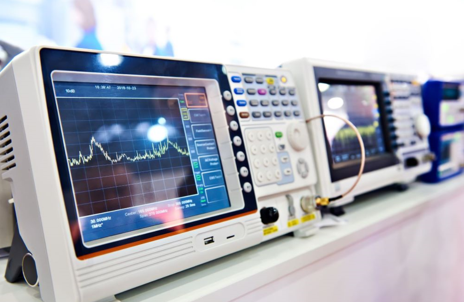
Noise phase is critical for clock systems because it can become random jitter after integration over the relevant offset frequency range. For EMI work, the spectrum analyzer is often a diagnostic instrument before formal chamber testing.
Recommended Reading: How to Calibrate a Spectrum Analyzer
Key Measurements and Assessment Criteria
Signal integrity testing becomes useful when every measurement is tied to a decision. A trace plot is not enough. The engineer needs a pass/fail threshold, a budget allocation, or a debug hypothesis.
Metric | Domain | Typical source | Engineering interpretation |
Eye height | Time domain | Scope or compliance tool | Vertical voltage margin at sampling point |
Eye width | Time domain | Scope or compliance tool | Timing margin after jitter and ISI |
Mask hits | Time domain | Compliance mask | Standard-specific pass/fail indicator |
RJ, DJ, TJ | Time domain/statistical | Jitter analysis | Random, deterministic, and total timing uncertainty |
Differential impedance | Time domain | Differential TDR | Controlled-impedance quality of the interconnect |
Insertion loss | Frequency domain | VNA | Signal attenuation through the channel |
Return loss | Frequency domain | VNA | Reflection caused by impedance mismatch |
Crosstalk coupling | Frequency or time domain | VNA, scope, BERT | Aggressor-to-victim interference |
BER | Link domain | BERT or built-in link counters | Actual error performance |
Skew | Time domain/layout | Scope, TDR, simulation | Relative delay between related signals |
Eye Diagram and Compliance Mask
The eye diagram is one of the most important views in signal integrity testing because it shows amplitude and timing margin together.
A clean eye has a large open region at the receiver sampling instant.
A degraded eye shows vertical closure from noise and loss, horizontal closure from jitter, and shape distortion from reflections or ISI.
A mask test is tied to the interface standard, measurement point, bit rate, test pattern, equalization state, and clock recovery model.
PCIe, Ethernet, DDR, and other standards define different electrical compliance methods. For PCIe compliance, the PCI-SIG ecosystem includes prescribed compliance fixtures and SigTest-based electrical analysis flows for card electromechanical testing.
Jitter Decomposition
Jitter should be interpreted according to its source:
Jitter component | Typical cause | Debug direction |
Random jitter | Thermal noise, oscillator phase noise, broadband noise, external radiation [5] | Clock source, PLL, power noise, bandwidth |
Data-dependent jitter | ISI, limited bandwidth, loss, reflections | Channel loss, equalization, impedance discontinuities |
Periodic jitter | Switching regulators, reference clocks, periodic coupling, crosstalk [5] | Spectrum analysis, power integrity, clock tree |
Duty-cycle distortion | Asymmetric rise/fall paths, threshold shifts | Driver configuration, termination, receiver threshold |
Bounded uncorrelated jitter | Crosstalk, unrelated switching aggressors | Aggressor isolation, routing, return path, shielding |
The goal is to identify which part of the timing budget is being consumed and which physical mechanism is responsible.
BER and Confidence
A BER threshold such as 1e-12 is useful only when the test duration and confidence are understood. At 10 Gb/s, transmitting 1e12 bits takes 100 seconds.
A zero-error run for 100 seconds at 10 Gb/s shows no observed errors in that interval, but it does not provide a 95 percent confidence upper bound of 1e-12. That requires about 3e12 bits, or about 300 seconds at 10 Gb/s, using the simple Poisson approximation.
PCB and Channel Factors
The measured signal is a direct consequence of physical design. A PCB layout can look correct geometrically and still fail because the electromagnetic structure is wrong.
Stackup and Ground Planes
Controlled impedance starts with stackup. Trace width, dielectric height, copper thickness, solder mask, dielectric constant, and reference plane continuity determine impedance and propagation delay.
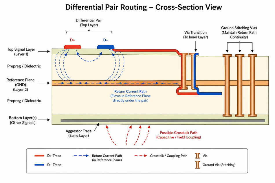
Ground planes are not just shielding layers. They provide the return-current path. A high-speed signal crossing a split plane, void, or reference transition without a nearby return via can create radiation, crosstalk, mode conversion, and ringing. Therefore, it’s a recommended practice to print ground areas between tracks or to add ground vias to decouple the electromagnetic fields.[1]
Vias and Launch Transitions
Vias are often the dominant discontinuities in dense high-speed designs. A via has barrel inductance, pad capacitance, anti-pad effects, reference plane transitions, and sometimes a stub.
At multi-gigabit speeds, a long via stub can create a resonant notch in insertion loss. Backdrilling, blind or buried vias, optimized anti-pads, ground via fences, and via-in-pad structures are common mitigation strategies.
TDR locates the discontinuity in high-speed designs
VNA measurements show whether the via structure creates return loss peaks, insertion loss notches, or mode conversion.
Suggested Reading: Via in Pad PCB Design
Differential Pair Routing
Differential routing requires controlled impedance, consistent spacing, length matching, symmetry, and a continuous reference path. Poor symmetry increases intra-pair skew and mode conversion.
Excessive spacing can reduce coupling and make the pair more sensitive to external fields. Excessively tight coupling can complicate routing and impedance control. The correct geometry depends on the stackup, standard, fabrication limits, and loss budget.
Power Distribution and Return Current
Power integrity failures can masquerade as signal integrity failures. A transmitter with noisy supply rails can produce excess jitter. A receiver with supply ripple can show apparent threshold noise.
A clock PLL with poor supply isolation can create phase noise spurs. Decoupling, plane design, regulator noise, and package power impedance all affect the measured eye.
Practical Engineering Workflow
A good signal integrity test workflow is planned before the PCB is fabricated. The worst time to decide how to measure a channel is after the first board fails.
1. Define the DUT and Compliance Point
Start by defining the DUT, the interface, the speed grade, the operating modes, and the exact point where the signal will be evaluated. For some standards, the compliance point is not the receiver pin. It may be a test fixture output, connector plane, package reference point, or software-defined measurement plane after de-embedding.
At this stage, it is essential to document hardware and design parameters like transmitter, package, breakout, PCB route, vias, connector, cable, receiver, and termination. Moreover, identify the type of testing required for different types of signals.
2. Build a Measurement Budget
Before measuring, create expected budgets for impedance, insertion loss, return loss, jitter, skew, crosstalk, and BER. Use the relevant PCIe, DDR, Ethernet, JEDEC, IEEE, or vendor requirements where applicable.
When the standard does not define a convenient board-level requirement, derive an internal budget from receiver sensitivity, transmitter capability, simulation, and margin policy.
3. Simulate Before Fabrication
Use pre-layout and post-layout simulation to predict risk. Pre-layout simulation and verification against known models helps choose stackup, topology, termination, connector class, and equalization strategy.[10]
Post-layout simulation uses extracted PCB interconnects, packages, vias, and S-parameter models. For SerDes links, IBIS-AMI simulation is commonly used to evaluate equalizer behavior and statistical eye margin.
4. Design Test Access and Fixtures
Test access must be engineered into the board. Add coaxial launch points, probe pads, SMA or SMPM connectors, removable terminations, loopback paths, calibration coupons, and impedance coupons where appropriate. Additionally, documenting the test setups prevents miscalculations and erroneous fabrication later.[10]
For VNA measurements, plan the calibration and de-embedding approach.
For high-speed oscilloscope measurements, plan probe loading, fixture bandwidth, termination, and clock recovery.
For BERT testing, plan loopback modes, test patterns, equalizer presets, stress conditions, and logging.
5. Calibrate, De-Embed, and Validate the Fixture
An important step is to calibrate the testing equipment frequently.[10] Measurement error can easily be mistaken for signal degradation. Before measuring the DUT, validate the fixture. Check insertion loss, return loss, repeatability, connector torque, cable stability, probe compensation, and calibration quality. Move the reference plane to the desired location using the appropriate de-embedding method.[7]
If a fixture has poor return loss or excessive insertion loss, it may dominate the result. A fixture that is acceptable for one data rate may be unusable for the next generation.
6. Measure, Correlate, and Debug
Start with the least invasive measurement that answers the most urgent question. TDR is suitable for links that do not train, and may quickly reveal an open, short, or severe impedance error.[2] For a link that trains but fails margin, eye diagram and BER testing may be more informative. A channel that simulates well but measures poorly can be well diagnosed using NA data, which can expose fabrication or connector differences.
Correlation is the key engineering loop:
Compare measured impedance to the stackup and field-solver target.
Compare measured S-parameters to extracted interconnect simulation.
Use measured S-parameters in channel simulation.
Compare simulated eye and jitter to oscilloscope measurements.
Compare predicted link margin to BER results.
Iterate the design, equalization, termination, or layout based on root cause.
7. Record Conditions and Pass/Fail Evidence
A passing screenshot is not enough. Record board revision, DUT serial number, temperature, voltage, firmware, equalizer state, data pattern, cable, fixture, probe, calibration file, de-embedding file, instrument bandwidth, clock recovery settings, and standard revision.
This information is essential when failures appear only on some boards or only after a layout change.
Debug Patterns for Engineers
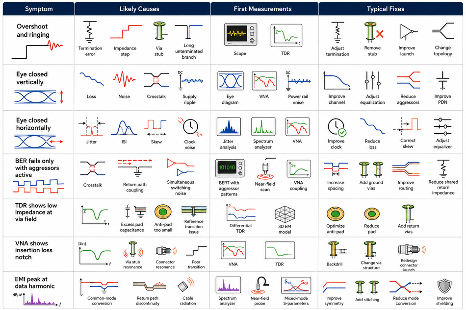
Signal integrity testing is a multi-dimensional area. Different types of integrity issues require different types of testing equipment and fixes. The important debug pattern is that no single plot gives the full answer. For instance:
A ringing waveform may be caused by an impedance mismatch, but the physical location usually comes from TDR.
A closed eye may be caused by attenuation, but the frequency signature comes from S-parameters.
A BER failure may be caused by jitter, but the root cause may be a switching regulator spur visible on a spectrum analyzer.
The following figure summarizes the debug patterns.
Compliance Context for Signal Integrity Testing
High-speed interfaces define electrical requirements so that transmitters, receivers, boards, connectors, and cables interoperate across vendors. PCIe, DDR, Ethernet, USB, MIPI, and proprietary SerDes links each have different assumptions about topology, equalization, reference clocks, channel loss, and compliance points.
PCIe Validation
PCIe validation is a good example of layered testing. A design may require transmitter electrical tests, receiver tolerance tests, link training checks, reference clock measurements, protocol analysis, and channel measurements.
For PCIe card electromechanical work, industry flows use compliance fixtures such as CBB and CLB boards along with SigTest-based analysis for electrical compliance.[8]
DDR Testing
DDR testing has a different character. A DDR interface is a source-synchronous parallel bus with clock, command, address, strobe, and data groups.
JEDEC DDR standards define the memory-device requirements and electrical framework; the board-level validation plan must also follow the controller and memory vendor guidance. JEDEC announced the JESD79-5C DDR5 SDRAM standard update in 2024, covering DDR5 reliability, security, and performance-related updates.[9]
SerDes Testing
SerDes testing is increasingly equalization-aware. At high data rates, the raw channel output may look poor before receiver equalization./
A link can have a closed eye at a passive observation point but still pass after equalization, or it can show a visually open eye and still fail receiver tolerance because of jitter, CDR behavior, or pattern-dependent effects.
Conclusion
Signal integrity testing turns high-speed PCB design from a layout assumption into measured engineering evidence. The essential task is to connect each failure mechanism to the instrument that can reveal it. An oscilloscope is suited for waveform, eye diagram, jitter, and mask behavior. TDR and TDT are used for impedance discontinuities and delay; a vector network analyzer monitors S-parameters, insertion loss, return loss, and crosstalk. A BERT is used for bit error rate, while a spectrum analyzer measures EMI, spurs, and phase noise.
The most effective workflow begins before layout with stackup planning, transmission line design, via modeling, fixture strategy, and simulation. It continues through calibrated measurement, de-embedding, correlation, and compliance testing against the correct PCIe, DDR, IEEE, JEDEC, or vendor-defined criteria. The goal is to preserve noise margins and timing margins across real boards, real interconnects, real operating conditions, and real manufacturing variation.
FAQ
1. What is signal integrity testing?
Signal integrity testing verifies that high-speed signals maintain enough voltage and timing margin as they travel through a PCB, connector, cable, package, or backplane. It includes waveform capture, eye diagram analysis, jitter measurement, impedance testing, S-parameter measurement, crosstalk evaluation, and BER testing.
2. Which instrument should I use first for signal integrity debug?
Use the instrument that best matches the failure symptom. If the waveform has overshoot, undershoot, or timing uncertainty, start with a high-bandwidth oscilloscope. If you suspect an impedance discontinuity, use TDR. If the channel has excessive loss or resonance, use a VNA. If the link trains but fails under traffic, use a BERT or internal error counters. If emissions or spurs are suspected, use a spectrum analyzer with appropriate probes.
3. How are TDR and VNA measurements different?
TDR is a time-domain method that shows impedance changes versus time or distance. It is excellent for locating discontinuities such as via stubs, connector transitions, trace width errors, and bad launches. A VNA is a frequency-domain instrument that measures S-parameters, including insertion loss, return loss, crosstalk, and mode conversion.
4. What BER is acceptable for a high-speed link?
The acceptable bit error rate depends on the interface standard, system reliability target, coding scheme, retry mechanism, and application. A common engineering threshold is 1e-12, but some systems require lower error rates or standard-defined receiver stress tests.
5. How does PCB layout affect signal integrity?
PCB layout controls impedance, delay, coupling, return current, via discontinuities, and loss. Trace geometry, stackup, ground planes, routing topology, differential pair symmetry, etc., affect the measured signal. Poor layout can produce ringing, crosstalk, EMI, mode conversion, jitter, and eye closure.
6. How do engineers test crosstalk?
Crosstalk can be tested in the time domain by driving aggressor channels while observing victim-channel noise, eye closure, or BER degradation. It can also be measured in the frequency domain using a multiport VNA to evaluate coupling terms between channels.
References
Signal Integrity White Paper. https://dl.cdn-anritsu.com/en-us/test-measurement/files/Technical-Notes/White-Paper/Signal_IntegrityWP.pdf
High Precision Time Domain Reflectometry. https://www.keysight.com/us/en/assets/7018-01179/application-notes-archived/5988-9826.pdf
What Is a Vector Network Analyzer and How Does It Work? https://www.tek.com/en/documents/primer/what-vector-network-analyzer-and-how-does-it-work
Impedance Matching. https://www.analog.com/en/resources/glossary/impedance-matching.html
Jitter Basics and Advanced. https://ieee.li/pdf/viewgraphs/jitter_basics_advanced.pdf
S-parameter Measurement Uncertainty on the R&S ZNA. https://www.rohde-schwarz.com/us/applications/s-parameter-measurement-uncertainty-on-the-rs-zna_56279-1103061.html
Accurate Test Fixture Characterization and De-embedding. https://cdn.rohde-schwarz.com.cn/pws/dl_downloads/dl_application/application_notes/1sl367/1SL367_0e_Test_Fixture_Characterization_and_De-embedding.pdf
PCI Express Design and Test from Electrical to Protocol. https://www.keysight.com/us/en/assets/7018-04665/brochures/5992-0340.pdf
JEDEC Updates JESD79-5C DDR5 SDRAM Standard. https://ddwg.jedec.org/news/pressreleases/jedec-updates-jesd79-5c-ddr5-sdram-standard-elevating-performance-and-security
Inside the Lab: Signal Integrity Testing Tools and Techniques. https://dev.to/fidus_systems/inside-the-lab-signal-integrity-testing-tools-and-techniques-15d1
in this article
1. Introduction2. Validation with Signal Integrity Testing 3. Failure Mechanisms in High-Speed PCB Interconnects4. SI Test Instruments and Methods5. Key Measurements and Assessment Criteria6. PCB and Channel Factors 7. Practical Engineering Workflow8. Debug Patterns for Engineers9. Compliance Context for Signal Integrity Testing10. FAQ11. References