SPI Protocol: Signals, Modes, Timing, and Implementation
The SPI protocol is a preferred protocol for short-distance communication between microcontrollers and peripherals. This reference covers the signals, the four SPI modes, multi-device wiring, timing, and real-world integration challenges you need to know to use it well.

Last updated on 05 Aug, 2026. 13 minutes read
Key Takeaways
The serial peripheral interface (SPI) is a synchronous, full-duplex protocol developed by Motorola in the 1980s.[1]
Four SPI modes, set by clock polarity (CPOL) and clock phase (CPHA), define when data is shifted and sampled.[2] Mode mismatch is the most common SPI bug.
SPI has no fixed maximum speed. Practical clock rates are often on the order of 10 MHz, and each device's datasheet sets the real limit.[2]
You can attach multiple slave devices with independent chip select lines or through a daisy-chain configuration that shifts data device to device.[3]
The Open Source Hardware Association now recommends SDO/SDI, PICO, and POCI in place of the legacy MOSI, MISO, and SS signal names.[4]
Introduction
The SPI protocol (serial peripheral interface) is one of the most widely used ways to move data between a microcontroller and the connected peripheral devices like sensors, ADCs, DACs, EEPROM and flash memory, displays, and SD cards. SPI bus is an integral part of most embedded systems.
SPI is a simple protocol, but incredibly fast, supporting high-speed data transfer. It’s a synchronous form of serial communication, so there is a shared clock signal for synchronous operations. Therefore, there is no need to establish a baud rate in advance, the way asynchronous protocols such as UART require.
That simplicity comes with trade-offs. SPI has no formal specification, no addressing, and no acknowledgement mechanism, so designers must read the datasheets carefully. But it’s versatile and efficient, making it a preferred option in various fields like robotics, IoT, and consumer electronics. This article discusses the architecture, signals, SPI modes, multi-slave topologies, timing, firmware, and integration challenges.
SPI Protocol Fundamentals
The serial peripheral interface is a synchronous serial bus developed by Motorola in the 1980s that became a de facto standard for connecting peripheral devices in embedded systems.[1] One master device (now usually called the controller) generates the clock and initiates every transfer to one or more slave devices (peripherals).
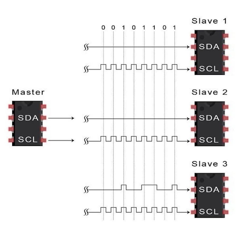
As a full-duplex communication protocol, SPI allows for simultaneous data transmission and reception, significantly boosting communication efficiency. Unlike I2C, which uses addressing schemes and can be slower due to its complexity, SPI’s simplicity and speed are key advantages, particularly in applications requiring rapid data transfer.
For example, in a digital camera, SPI facilitates fast communication between the microcontroller and the image sensor, ensuring quick and efficient image processing. This efficiency and speed are why SPI is widely used in consumer electronics, industrial systems, and IoT devices.
Three properties define SPI:
Synchronous: A dedicated clock line synchronizes every bit, unlike UART, which relies on both ends independently timing bits against an agreed baud rate.[1]
Full-duplex: Data flows in both directions at once on separate lines. Every clock cycle exchanges one bit in each direction.
Unstandardized: SPI differs from I2C, as it does not define a standard communication format.[1] Frame length, bit order, and command structure are set by each device. For example, Linux supports word sizes of 8, 12, or 20 bits per word, not just bytes.[2]
In SPI, each bit needs its own clock period. Therefore, SPI is serial rather than parallel communication. So, it replaces the need for wide parallel bus interfaces with a few wires that still support high-speed data transfer over short distances, typically centimeters of board trace.
Recommended Reading: What is SPI? How the Serial Peripheral Interface Works
SPI Signals and Master-Slave Architecture
A standard 4-wire SPI bus uses a master-slave architecture with four signals.[1] Here is a quick breakdown.
Signal | Legacy name | Updated name | Direction | Function |
Serial clock | SCLK, SCK, CLK | SCK / SCLK (unchanged) | Master to slave | Clock signal that synchronizes every bit |
Data, master to slave | MOSI (master out slave in) | PICO or SDO/SDI | Master to slave | Command and write data |
Data, slave to master | MISO (master in slave out) | POCI or SDI/SDO | Slave to master | Response and read data |
Device enable | SS (slave select) | CS (chip select) | Master to slave | Active-low line that enables one peripheral |
The master device generates the serial clock (SCLK) and drives chip select. The chip select line is normally held high, which disconnects the peripheral from the bus. It pulls the pin low (active low) to select the device for the transaction.[5]
MOSI carries data from the master to the slave device
MISO carries data back.
Because both lines are active during the same clock cycles, SPI achieves full-duplex transfer by design.
Modern Naming for SPI Signals
The OSHWA resolution on SPI signal names deprecates MOSI, MISO, and slave select in favor of controller/peripheral language.[4]
Single-role devices label their pins as SDO (Serial Data Out) and SDI (Serial Data In).
Dual-role devices use PICO (Peripheral In, Controller Out) and POCI (Peripheral Out, Controller In).

Vendors have adopted the change at different speeds, and Arduino uses the variant COPI/CIPO for the same lines.[6] Recent vendor documentation, like the one from Texas Instruments, is written entirely in PICO/POCI terms.[1]
However, modern datasheets use both vocabularies. So, it’s a good idea to learn the mapping:
MOSI = PICO
MISO = POCI
SS = CS
Suggested Reading: Arduino Nano Pinout: Complete Technical Reference
Data Movement with Shift Registers
SPI comprises two shift registers that exchange data during serial transmission. On each clock cycle, the master shifts one bit out on MOSI and the slave shifts one bit out on MISO. After 8 clock cycles (for an 8-bit frame), the two registers have effectively swapped data.
Consider an example of a digital audio system. The microcontroller sends audio data to a digital-to-analog converter (DAC) while concurrently receiving status information from the DAC. It minimizes delay and maximizes throughput, which is crucial in real-time applications.
The transfer order is configurable. Most SPI chips send the most significant bit (MSB) first, but devices can specify least significant bit (LSB) first, so check the datasheet before assuming MSB or LSB order.[6]
A minimal transaction looks like this:
The master configures clock polarity, clock phase, speed, and bit order for the target peripheral.
The master pulls the chip select line low.
The master toggles the clock; each rising edge or falling edge shifts and samples one bit on MOSI and MISO.
After the final bit, the master returns the chip select pin high, ending the transaction.
Setting Up SPI Modes with Clock Polarity and Phase
The SPI protocol lets the master choose when data is driven and when it is sampled relative to the clock. These decisions are managed by two bits:
Clock Polarity (CPOL) - Shows the idle state of the clock.
Clock Phase (CPHA) - Determines which clock edge samples data
Based on the combination of the two bits, there are four SPI modes.[3] The following table summarizes the clock polarity and data shifting:
Mode | CPOL | CPHA | Clock idle level | Data sampled on | Data shifted on |
Mode 0 | 0 | 0 | Low | Rising edge | Falling edge |
Mode 1 | 0 | 1 | Low | Falling edge | Rising edge |
Mode 2 | 1 | 0 | High | Falling edge | Rising edge |
Mode 3 | 1 | 1 | High | Rising edge | Falling edge |
Mode 0 (CPOL = 0, CPHA = 0) is the most common configuration in practice. As an example of how a real part specifies this, TI's TXE8116 I/O expander uses a fixed 24-bit frame, MSB first, in SPI mode 0, with data captured on the rising edge of SCLK and driven on the falling edge.[1]
The master must match the mode the slave device expects. For example, in a temperature monitoring system, selecting the correct SPI mode aligns the microcontroller with the sensor's communication requirements, ensuring accurate temperature readings.
The Linux kernel documentation adds a subtle requirement. According to that, the clock must already be at its correct idle level before chip select goes active, or CPHA = 0 devices can mis-sample the first bit.[2]
Connecting Multiple Peripheral Devices
One master can serve several peripherals. There are three wiring options. Each comes with distinct trade-offs.
Independent Chip Select Lines
In the regular configuration, all slave devices share SCLK, MOSI, and MISO, and each gets a dedicated chip select line from the master. However, only one line may be active at a time. So, for instance, if two chip selects are low together, the data on the MISO line is corrupted because two peripherals drive it at once.[2]

The cost is pin count. Each added peripheral consumes another GPIO on the master, which is why designs with many devices use a multiplexer for chip select generation or move to SPI-controlled parts.
Analog Devices documents a switch-matrix design where SPI control cuts the required GPIOs from 16 to 7.[2]
Daisy-Chain Configuration
Daisy-chaining connects the POCI output of one device to the PICO input of the next, with one shared chip select for the whole chain. Data shifts through every device in series. So, to reach any one peripheral, you must transmit enough bits to pass through all of them.[1]
The advantage of daisy-chaining is that it reduces the chip-select lines and somewhat reduces hardware complexity.

The chain works like a long shift register, so there will be obvious latency through the chain. This latency cost is proportional to position in the chain. In an 8-bit system, 24 clock pulses are needed to deliver data to the third device, versus 8 in the regular configuration.[3]
Moreover, not all peripheral devices support daisy-chaining, so confirm it in the datasheet before committing your board layout to it.
3-Wire, Dual, Quad, and Octal SPI
Some devices combine PICO and POCI into one bidirectional data line, called 3-wire SPI (SCLK, CS, and DIO).[1] This halves the data wiring at the cost of full-duplex operation.
Memory chips push the opposite direction: more data lines. Dual, quad, and octal SPI move 2, 4, or 8 bits per clock to speed up flash memory reads. JEDEC standardized this evolution as xSPI (JESD251), which delivers up to 400 megabytes per second of raw throughput for nonvolatile memory in computing, automotive, IoT, and mobile systems, while keeping limited backward compatibility with legacy SPI.[7] The latest revision, JESD251D, was published in May 2026.

SD cards are a related special case. Every MMC and SD memory card supports an SPI access mode, which is why small embedded systems can log data to an SD card over four wires instead of a dedicated card interface.[2]
SPI vs I2C vs UART
Choosing between SPI, I2C, and UART is one of the first architecture decisions in an embedded design. The following table summarizes the key differences[1]:
Feature | SPI | I2C | UART |
Communication type | Synchronous | Synchronous | Asynchronous |
Duplex | Full-duplex | Half-duplex | Full-duplex |
Clock signal | Yes | Yes | No (baud rate agreed in advance) |
Addressing | Chip select line | In-protocol addresses | Not applicable (point to point) |
Relative speed | High | Medium | Low |
Signal count | 4 lines, plus 1 CS per added device | 2 lines, any device count | 2 lines, two devices only |
Simply put, the use cases for each can be summarized as:
SPI is best for full-duplex, high data-rate, and multiple peripherals like ADCs, sensors, and displays.
I2C is suited for hardware-constrained applications where a smaller number of pins is more important than transmission speed.
UART applies to point-to-point links like GPS modules, debug consoles, etc.

Generally, UART speed is expressed as a baud rate because it is asynchronous. SPI speed is simply the serial clock frequency the master generates.
Recommended Reading: I2C vs SPI vs UART: A Comprehensive Comparison
SPI Operational Considerations
How Fast can the SPI protocol go?
SPI defines no speed ceiling. Real buses commonly run on the order of 10 MHz, and individual parts specify their own limits, so it’s essential to consult the product datasheet for the clock frequency specification.[2,3]
The maximum clock speed of SPI is constrained by the hardware capabilities of the master and slave devices. Concrete timing numbers make the constraints tangible. TI's TXE8116 specifies a 100 ns SPI clock period (10 MHz), chip select setup and hold times of at least 50 ns, and output valid within 27 ns of the clock edge.[1]
Timing and Layout Guidelines
As the clock speed increases, maintaining signal integrity becomes more difficult, potentially leading to data errors. But a few practical rules can ensure reliability in a fast SPI bus:
Verify setup and hold: Before increasing the clock speed, verify that the slave's minimum chip select setup and hold times and its maximum clock frequency.
Never toggle chip select mid-frame: Deasserting CS partway through a frame can corrupt the transaction. Hold it low for the full sequence.[1]
Guard signal integrity at speed: As clock rates climb into the tens of MHz, trace length, stubs, and ground return paths start to matter. Keep SCLK traces short and matched to the data lines.
Ensure Cable shielding for EMI Protection: High-speed signals are prone to Electromagnetic interference. Ensuring EMI protection helps preserve signal integrity.
Check drive conflicts: On shared buses, confirm only one chip select is active and that inactive peripherals release the POCI line to high impedance. TI's part specifies POCI entering high-Z within 50 ns of CS deassertion.[1]
Recommended Reading: Signal Integrity Testing for High-Speed PCB Design
Implementing SPI in Firmware
Every microcontroller vendor ships an SPI peripheral driver, and hobbyist platforms wrap it in a simple API. The Arduino SPI library is a representative example of the universal pattern[6]:
Step | Command | Description |
Configure the port for the target device | SPI.beginTransaction(SPISettings(14000000, MSBFIRST, SPI_MODE0)); | Sets a 14 MHz maximum clock, MSB-first order, and mode 0. Arduino automatically uses the fastest supported speed at or below your figure. |
Pull the chip select pin low | - | - |
Call the function to transfer bytes | SPI.transfer() | Call for each byte. Each call clocks one byte out while reading one byte in, reflecting SPI's full-duplex nature. |
Raise chip select and end transmission | SPI.endTransaction() | Releases the bus for other libraries |
The same sequence maps to register-level firmware on any MCU:
Configure the control register (mode, order, clock divider), assert CS pin.
Feed the data register and wait for the shift to complete.
Deassert the CS pin.
On Linux systems, the kernel exposes the identical concepts (mode, word size, maximum clock) through its SPI subsystem and spidev interface.[2] On classic 16 MHz Arduino boards, the achievable clock ranges from 8 MHz down to 125 kHz via the clock divider, a useful reminder that the master, not the protocol, sets the pace.[5]
Suggested Reading: Microcontroller Programming: Mastering the Foundation of Embedded Systems
Debugging SPI buses
When an SPI link fails, the fault is almost always configuration, not hardware. Work through this checklist:
Mode mismatch: Confirm CPOL and CPHA against the slave datasheet. A device expecting mode 0 will return garbage in mode 3, since both edges are inverted.
Bit order: Verify MSB versus LSB first.
Chip select discipline: Confirm CS is low for the entire frame and that no second device is selected.
Clock rate: Drop to 1 MHz or lower while debugging; if the link recovers, you have a timing or signal integrity problem, not a logic problem.
Look at the wires: A logic analyzer decodes SPI traffic directly and shows mode, order, and framing errors at a glance. An oscilloscope complements the logic analyzer by revealing analog problems, like slow edges, ringing, or a clock idle level that disagrees with your CPOL setting.
Where SPI Is Used
SPI's mix of speed, simplicity, and low pin count makes it the default for short-distance communication inside a product. The typical applications of SPI are datalogging applications, sensor integration, smart home and IoT applications, etc. The typical use of the SPI protocol in these applications is:
Sensors: IMUs, pressure and temperature sensors, and magnetometers, where SPI's clock rates support kilohertz sample rates that would saturate I2C.
Data converters: DCs and DACs, which stream conversion results or waveform samples every few microseconds.
Memory: EEPROM for configuration, NOR and NAND flash memory for code and data storage, plus FRAM and MRAM. This segment drove the quad and octal xSPI evolution.[7]
Storage: SD cards in SPI mode for logging in low-cost embedded systems.
Displays and drivers: TFT and OLED display controllers, LED drivers, and digital potentiometers.
Interface expansion: GPIO expanders, switch matrices, and shift registers that let one microcontroller control devices far beyond its native pin count.
Real-World Integration Challenges and Solutions
SPI systems offer a simplified option for embedded system designers for high-speed data acquisition. However, there are a few integration challenges when it comes to real-world applications. Here are a couple of examples:
Integrating SPI in a Multi-Device Industrial Control System
In an industrial control system, integrating SPI with multiple sensors and actuators presented challenges in ensuring signal integrity and managing bus contention. The environment’s electrical noise interfered with the SPI signals, leading to data corruption.
Solution
Shielded Enclosures: Placing SPI components in shielded enclosures reduced EMI and improved signal integrity.
Optimized PCB Layout: Redesigning the PCB with controlled impedance traces and solid ground planes minimized signal reflections.
Dedicated Chip Select Lines: Allocating individual chip select lines for each sensor and actuator prevented bus contention, ensuring reliable communication.
Recommended Reading: How to Design a PCB Layout: A Comprehensive Guide
High-Speed Data Acquisition System
A high-speed data acquisition system required integrating SPI with multiple high-speed ADCs (Analog-to-Digital Converters). Ensuring accurate timing and high data transfer rates was crucial.
Solution
Clock Synchronization: Using a common clock source for the master and ADCs ensured precise synchronization.
DMA Implementation: Implementing DMA reduced CPU overhead and enabled efficient data transfers, meeting the high-speed requirements.
Conclusion
The SPI protocol has been a preferred option in embedded designs because it is fast, predictable, and offers full-duplex exchange between a master and nearby peripherals over a minimal set of wires. Its lack of a formal standard is both its flexibility and its sharp edge, so the datasheet is always your source of truth for mode, speed, frame format, and timing.
By mastering the fundamentals of SPI protocol, engineers and embedded system designers can design reliable high-speed interfaces with minimal hardware complexity
Frequently Asked Questions
1. Is SPI faster than I2C?
Yes, in practice. Standard I2C tops out at hundreds of kilobits per second in its common modes, while SPI buses routinely run at clock rates of 10 MHz and beyond, and SPI's full-duplex operation moves data both directions simultaneously. The trade-off is more wires and no built-in addressing.
2. What is SPI mode 0?
Mode 0 means CPOL = 0 and CPHA = 0: the clock signal idles low, data is sampled on the rising edge, and data is shifted out on the falling edge. It is the most widely supported of the four SPI modes.
3. What do MOSI and MISO stand for?
MOSI is master out slave in, the line carrying data from the master to the peripheral. MISO is master in slave out, the return line. Updated terminology replaces these with PICO (Peripheral In, Controller Out) and POCI (Peripheral Out, Controller In), or SDO and SDI on single-role devices.
4. How many devices can share one SPI bus?
There is no protocol-defined limit. Each added slave device needs either its own chip select line or a position in a daisy chain, so the practical ceiling is set by available GPIOs, bus capacitance, and timing margin at your chosen clock rate.
5. Does SPI use a baud rate?
Not in the UART sense. Because SPI is synchronous, the master's serial clock explicitly times every bit, so there is no pre-agreed baud rate; you simply set the clock frequency within the slave's specified limit.
6. Is SPI full-duplex or half-duplex?
Standard 4-wire SPI is full-duplex: every clock cycle transfers one bit on MOSI and one on MISO simultaneously. The 3-wire variant, which shares a single data line, is half-duplex.
References
Texas Instruments, Understanding the SPI Bus (SBOA621), August 2025
Analog Devices, Introduction to SPI Interface, Analog Dialogue
Open Source Hardware Association, A Resolution to Redefine SPI Signal Names
The Linux Kernel documentation, Overview of Linux kernel SPI support
JEDEC, eXpanded Serial Peripheral Interface (xSPI) for Nonvolatile Memory Devices, JESD251D, May 2026
Arduino, Arduino and Serial Peripheral Interface (SPI) documentation
in this article
1. Key Takeaways2. Introduction3. SPI Protocol Fundamentals4. SPI Signals and Master-Slave Architecture5. Setting Up SPI Modes with Clock Polarity and Phase6. Connecting Multiple Peripheral Devices7. SPI vs I2C vs UART8. SPI Operational Considerations 9. Implementing SPI in Firmware10. Where SPI Is Used11. Real-World Integration Challenges and Solutions12. Conclusion13. Frequently Asked Questions14. References