PCB Potting: Fortifying Electronics Against Extreme Elements
An in-depth review of PCB potting, its applications, materials, technologies, and the AI-powered advancement in potting techniques and material engineering.

28 Oct, 2024. 14 minutes read
Introduction
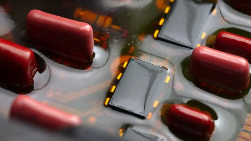
PCB potting is a critical process in electronics manufacturing that involves encapsulating printed circuit boards (PCBs) and their components in a specialized compound.. It’s a significant protection technique that has grown exponentially in recent years, driven by the increasing demand for robust electronics in harsh environments. From the aerospace and automotive industries to medical devices and underwater equipment, PCB potting is becoming indispensable. As electronic systems become more complex and are deployed in increasingly challenging conditions, the role of PCB potting in safeguarding these vital components continues to expand, making it a cornerstone of modern electronics manufacturing.
PCB potting provides superior protection against environmental factors such as moisture, chemicals, and physical stress, ensuring the longevity and reliability of electronic devices. While conformal coating offers a thin protective layer, potting fully encases the PCB, offering comprehensive shielding.
Suggested Reading: Understanding Conformal Coating vs Potting or Encapsulation
PCB Potting Demystified
PCB potting is essential for modern-day electronics as sophisticated component assembly techniques have ensured more compact and performance-oriented PCB designs. Hence, in cutting-edge applications, component failure due to environmental conditions can prove to be too costly.
Therefore, when the components are well-protected with advanced PCB potting techniques, it ensures reliability and durability in printed circuit boards.
The Potting Process Unveiled
PCB potting is a meticulous process requiring precision and attention to detail. Therefore, understanding each step is crucial for achieving optimal protection for electronic components. The potting process involves several key stages, each playing a vital role in the final product's quality and effectiveness.
PCB Preparation:
Clean the PCB thoroughly to remove contaminants and ensure proper adhesion.
Ensure proper PCB inspection for any damaged components or solder joints.
Apply masking to areas that should not be potted, such as connectors or test points.
Mold Selection and Preparation:
Choose an appropriate mold based on the PCB size and desired potting shape.
Apply release agent to the mold to facilitate easy removal of the cured potting compound.
Position the PCB securely within the mold, ensuring proper orientation.
Potting Compound Preparation:
Select the appropriate potting compound based on the application requirements.
Mix the compound according to the manufacturer's specifications, paying close attention to ratios and mixing times.
De-gas the mixture to remove air bubbles that could compromise the potting integrity.
Compound Application:
Pour or inject the prepared compound into the mold, ensuring even distribution around the PCB.
Use vacuum or pressure techniques to eliminate voids and ensure complete encapsulation.
Monitor the fill level to achieve the desired potting thickness.
Curing Process:
Allow the potting compound to cure according to the specified time and temperature conditions.
For some compounds, use heat curing to accelerate the process and enhance properties.
Monitor the curing process to ensure complete solidification without overheating components.
Post-Cure Inspection and Finishing:
Remove the potted PCB from the mold carefully.
Inspect for any defects such as voids, cracks, or incomplete coverage.
Trim excess material and perform any necessary finishing operations.
Potting System Essentials
A successful PCB potting system relies on three critical components: potting compounds, molds, and dispensing equipment. Each element plays a vital role in creating a robust and effective protective encapsulation for electronic components.
Potting Compounds
Potting compounds are the heart of the system, providing the actual protective barrier. These specialized materials come in various formulations, including epoxies, silicones, and polyurethanes, each offering unique properties suited to different applications. The choice of compound significantly influences the final product's thermal, electrical, and mechanical characteristics.
Molds
Molds are crucial in shaping the potting compound around the PCB. They can be made from various materials such as silicone rubber, metal, or plastic, depending on the production volume and required precision. The mold design must account for factors like compound shrinkage, air entrapment prevention, and ease of PCB removal post-curing.
Dispensing Equipment
Dispensing equipment ensures accurate and consistent application of the potting compound. This can range from simple manual syringes for low-volume production to sophisticated automated systems for high-volume manufacturing. Advanced dispensing systems often incorporate precise volume control, vacuum degassing, and multi-component mixing capabilities.
The synergy between these components is essential for creating effective potting systems. The compound must be compatible with both the mold material and the PCB components. The dispensing equipment must handle the compound's viscosity and curing characteristics. The mold design must accommodate the dispensing method while ensuring proper coverage and curing of the compound.
Component | Types | Key Properties | Considerations |
Potting Compounds | Epoxy, Silicone, Polyurethane | Thermal conductivity, Dielectric strength, Flexibility, Chemical resistance | Application environment, Curing time, Exothermic reaction |
Molds | Silicone rubber, Metal, Plastic | Durability, Precision, Thermal stability | Production volume, Compound compatibility, Complexity of PCB shape |
Dispensing Equipment | Manual syringes, Automated systems | Accuracy, Speed, Mixing capability | Production volume, Compound viscosity, Curing time |
The careful selection and integration of these components are crucial for achieving optimal protection for PCBs. Engineers must consider factors such as the operating environment, production volume, and specific protection requirements when designing a potting system. By understanding the links between compounds, molds, and dispensing equipment, manufacturers can create potting solutions that effectively shield electronic components from a wide range of environmental threats.
The Science of Potting Materials
Compound Chemistry Deep Dive
Understanding the chemical composition of potting compounds is crucial for selecting the right material for specific PCB protection needs. The three major types of potting compounds - epoxy, silicone, and polyurethane - each have unique chemical structures that directly influence their properties and performance in electronic applications.
Epoxy Compounds
Epoxy compounds, with a typical chemical formula of C21H25ClN2O5S, are characterized by their strong cross-linked molecular structure. This structure contributes to epoxy's excellent thermal conductivity, ranging from 0.2 to 0.6 W/m·K.
The presence of aromatic rings and multiple functional groups in the epoxy molecule provides high resistance to chemicals and moderate flexibility. Epoxy's molecular structure can be visualized as a network of interconnected rings and chains, forming a rigid yet durable matrix.
Silicone Compounds
Silicone-based potting compounds, represented by the formula (C4H10OSi)2, feature a backbone of alternating silicon and oxygen atoms with organic groups attached to the silicon. This unique structure gives silicone its characteristic high flexibility and excellent resistance to weathering.
The Si-O bonds contribute to silicone's moderate thermal conductivity (0.1-0.2 W/m·K) and its ability to maintain properties over a wide temperature range. Imagine a silicone molecule as a flexible chain with silicon atoms at its core, surrounded by organic groups that can easily rotate and bend.
Recommended Reading: Silicon Semiconductor: A Comprehensive Guide to Silicon and its Use in Semiconductor Technology
Polyurethane Compounds
Polyurethane compounds, with a typical formula of C25H42N2O6, are formed by the reaction of diisocyanates with polyols. This reaction creates a polymer with urethane linkages (-NH-COO-) that contribute to polyurethane's very high flexibility and good chemical resistance.
The thermal conductivity of polyurethane (0.16-0.25 W/m·K) falls between that of epoxy and silicone, making it a versatile choice for various applications. Visualize polyurethane as long, intertwined chains with regularly spaced urethane groups acting as flexible joints.
Suggested Reading: What are flexible filaments and which one should you choose?
The chemical structure of these compounds directly influences their key properties:
Thermal Conductivity: Epoxy's tightly cross-linked structure allows for better heat transfer, resulting in higher thermal conductivity compared to silicone and polyurethane.
Flexibility: The long, flexible Si-O backbone in silicone and the urethane linkages in polyurethane provide greater flexibility compared to the more rigid epoxy structure.
Chemical Resistance: Epoxy's dense cross-linking offers high chemical resistance, while silicone's inert Si-O backbone provides excellent weathering resistance. Polyurethane's urethane bonds offer good overall chemical resistance.
Adhesion: The presence of polar groups in epoxy and polyurethane molecules contributes to their strong adhesion properties, while silicone's non-polar nature results in lower adhesion strength.
Understanding these chemical structures and their relationship to material properties is essential for engineers and designers when selecting the most appropriate potting compound for specific PCB protection requirements.
Frontier Materials for Extreme Conditions
As electronic devices are deployed in increasingly challenging environments, traditional potting compounds often fall short. This has led to the development of frontier materials designed to withstand extreme conditions while providing superior protection for PCBs. These advanced materials are pushing the boundaries of what's possible in electronics protection, enabling new applications in industries such as aerospace, deep-sea exploration, and high-temperature industrial processes.
High-Temperature Resistant Materials - Advanced ceramic-filled silicones and polyimides are at the forefront of high-temperature potting solutions. These materials can withstand temperatures exceeding 300°C, making them ideal for automotive engine compartments and aerospace applications.
Ceramic-filled silicone exhibits the following temperature-related properties:
Temperature resistance up to 350°C
Excellent thermal conductivity (up to 1.5 W/m·K)
Low outgassing in vacuum environments
Resistance to thermal shock and vibration
Polyimide potting compound characteristics:
Continuous operating temperature up to 250°C with short-term exposure up to 400°C
Outstanding electrical insulation properties
High mechanical strength and dimensional stability
Excellent adhesion to various substrates
Industry example: In jet engine control systems, ceramic-filled silicones protect sensitive electronics from extreme heat and vibration, ensuring reliable operation at altitudes where temperatures can fluctuate dramatically.
Chemically Inert Solutions - Fluoropolymer-based potting compounds offer unparalleled resistance to harsh chemicals, making them essential in corrosive environments such as chemical processing plants and oil refineries.
Fluoropolymer potting material exhibits the following properties:
Resistance to a wide range of acids, bases, and solvents
Operating temperature ranges from -200°C to +200°C
Low moisture absorption
Excellent electrical insulation properties
Industry example: In offshore oil platforms, fluoropolymer potting compounds protect subsea control systems from saltwater intrusion and hydrocarbon exposure, ensuring long-term reliability in these harsh marine environments.
Optically Clear Potting Solutions - Transparent potting materials are crucial for applications where visual inspection or light transmission is necessary, such as in LED assemblies and optical sensors.
Optically clear silicone properties:
Light transmittance >90% in the visible spectrum
Refractive index matching capabilities
UV and weather resistance
Flexibility to accommodate thermal expansion
Transparent epoxy characteristics:
High clarity and low yellowing over time
Excellent adhesion to glass and plastic substrates
Good thermal and electrical insulation properties
Ability to be polished to an optical finish
Industry example: In automotive LED headlights, optically clear silicones encapsulate the LED arrays, protecting from moisture and vibration while allowing maximum light output and heat dissipation. In addition to high transparency, they are more resistant to cracks and harsh temperature conditions.
Further Reading: Driving Efficiency: Exploring Lightweight Materials in Automotive Applications
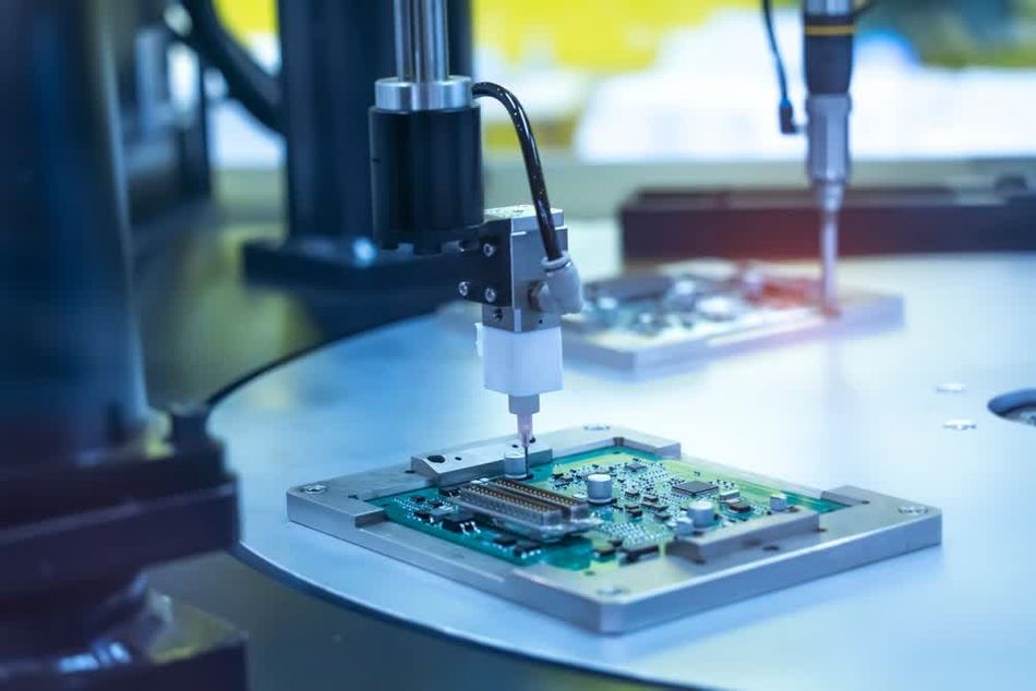
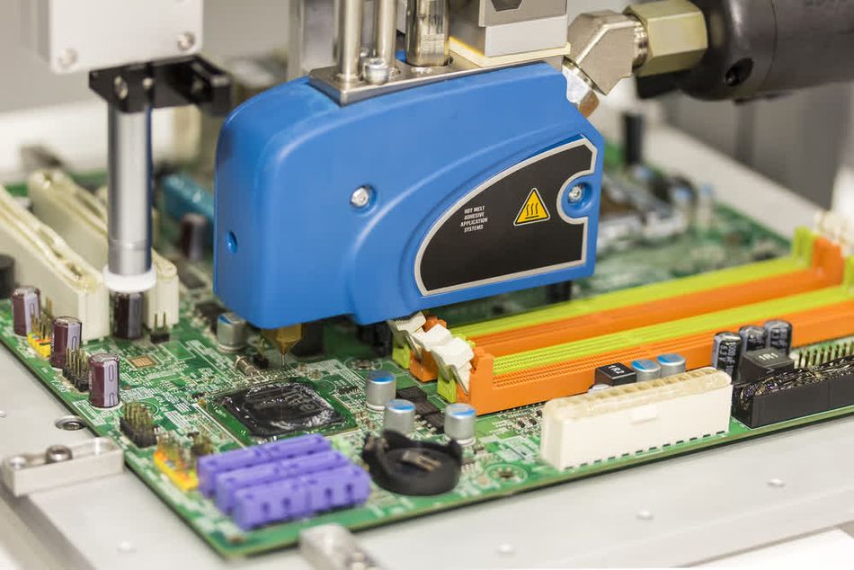
Innovative Potting Technologies
AI-Driven Automated Systems
The PCB potting industry is witnessing a revolutionary shift with the integration of AI-driven automated systems. These cutting-edge technologies are transforming the potting process, offering unprecedented levels of precision, consistency, and efficiency.
Robot-Driven Potting Techniques
Modern automated potting systems utilize advanced robotics and computer vision to achieve highly accurate dispensing of potting compounds. These systems can precisely control factors such as dispensing rate, volume, and pattern, ensuring optimal coverage and minimizing waste.
In a typical robotic setup, a robot precisely dispenses a set amount of potting material onto electronic components, sealing them from environmental factors like dust, dirt, and moisture. This automated process significantly speeds up production, ensuring consistency and efficiency in the assembly line.
Quality Control with Machine Vision
AI-driven systems excel in quality control. Advanced image recognition algorithms can detect even minute imperfections in the potting process, such as air bubbles or incomplete coverage, at speeds far surpassing human capability. This ensures a consistently high-quality output, crucial for industries where electronic failure is not an option.
Moreover, AI algorithms analyze real-time data from sensors monitoring viscosity, temperature, and curing rates, making micro-adjustments to maintain ideal potting conditions throughout the process. For instance, modern electronics rely on complex surface-mount technology, making manual inspection of solder joints impractical. Automated Optical Inspection (AOI) systems, powered by deep learning, can accurately detect defects by analyzing images of PCBs. This early detection significantly improves product quality and reduces production costs.
Machine learning plays a crucial role in enhancing the capabilities of these systems. By analyzing vast amounts of historical data from previous potting operations, ML algorithms can predict potential issues before they occur and suggest preventive measures. This predictive maintenance approach significantly reduces downtime and improves overall production efficiency.
Suggested Reading: Spotlight on Innovations in Edge Computing and Machine Learning: Predictive Maintenance
Self-Optimizing Potting Systems
The integration of AI has also led to the development of self-optimizing potting systems. These systems can learn from each potting cycle, continuously refining their processes to achieve optimal results. For instance, they can automatically adjust dispensing parameters based on changes in ambient temperature or variations in PCB designs, ensuring consistent quality across different production batches.
While the benefits of AI-driven automated systems are significant, it's important to understand how they compare to traditional manual potting techniques. The following table provides a comparison:
Technique | Advantages | Disadvantages |
Manual Potting | Flexibility in process, lower initial costs, simpler setup | Higher labor costs, potential for human error, slower production rates |
Automated Potting | High precision, consistency in application, faster production speeds | Higher initial investment, complexity in setup, less flexibility |
These comparisons suggest that automated systems require a higher initial investment and are more complex to set up. However, they offer substantial benefits in terms of precision, consistency, and production speed. These advantages make AI-driven automated systems particularly valuable for high-volume production or applications requiring extremely precise potting.
The adoption of AI-driven automated systems in PCB potting represents a significant leap forward in electronic component protection. As these technologies continue to evolve, we can expect even greater levels of precision, efficiency, and reliability in the potting process, ultimately leading to more robust and durable electronic devices across various industries.
Nano-Enhanced Compounds: The Future of Potting
Nano-enhanced potting compounds represent a significant leap forward in PCB protection technology. These advanced materials incorporate nanoparticles—typically ranging from 1 to 100 nanometers in size—into traditional potting resins, resulting in compounds with dramatically improved properties. The integration of nanomaterials such as carbon nanotubes, graphene, and metal oxide nanoparticles is revolutionizing the performance capabilities of potting compounds.
Enhanced Thermal Performance
Nanoparticles enhance the thermal properties of potting compounds by creating more efficient pathways for heat dissipation. For instance, the addition of aluminum oxide nanoparticles can increase thermal conductivity by up to 400% compared to conventional compounds. This improvement allows for better heat management in high-power electronic devices, potentially extending their lifespan and reliability.
High Physical Strength
Mechanically, nano-enhanced compounds exhibit superior strength and durability. The incorporation of silica nanoparticles can significantly increase the tensile strength and impact resistance of epoxy-based potting materials. This enhanced mechanical performance is crucial for electronics operating in high-vibration or shock-prone environments, such as automotive or aerospace applications.
Superior Conductivity
Electrically, nanoparticles can be used to tailor the dielectric properties of potting compounds. Carbon nanotubes, for example, can be used to create electrically conductive pathways within the potting material, allowing for controlled dissipation of static charges or even electromagnetic shielding. Conversely, certain nanoparticles can enhance the insulating properties of the compound, improving its breakdown voltage and overall electrical reliability.
Ongoing research in nano-enhanced potting compounds is focusing on several promising areas:
Self-healing properties: Incorporation of microencapsulated healing agents and nanoparticle catalysts that can automatically repair microcracks in the potting material.
Stimuli-responsive behavior: Development of compounds that can change properties in response to external stimuli like temperature or electric fields.
Biocompatibility: Creation of nano-enhanced potting materials suitable for medical implants and other bioelectronic devices.
Environmental sustainability: Research into biodegradable nanoparticles and eco-friendly production methods for nano-enhanced compounds.
Some additional advantages of nano-enhanced potting compounds include:
Potential for multifunctional capabilities (e.g., self-healing, EMI shielding)
Reduced coefficient of thermal expansion, leading to better thermal cycling performance
Improved adhesion to substrate materials
Potential for reduced weight and volume compared to traditional compounds
Enhanced chemical resistance and barrier properties
The integration of nanotechnology into potting compounds is opening new possibilities for electronic protection and functionality. As research progresses and manufacturing techniques improve, nano-enhanced potting compounds are poised to become a standard solution for high-performance electronic applications across various industries.
Conclusion
PCB potting has emerged as a cornerstone technology in modern electronics, providing critical protection against environmental hazards and enhancing overall device reliability. From traditional epoxy and silicone compounds to cutting-edge nano-enhanced materials, the evolution of potting technologies has kept pace with the increasing demands of electronic applications. The integration of AI and machine learning in automated potting systems is revolutionizing manufacturing processes, offering unprecedented precision and efficiency.
As electronics continue to penetrate more challenging environments, from deep-sea exploration to space applications, the role of advanced potting solutions becomes ever more crucial. The future of PCB potting lies in smart, adaptive materials and processes that can offer not just protection, but also enhanced functionality, sustainability, and integration with emerging technologies like IoT and 5G. This continuous innovation in PCB potting will undoubtedly play a pivotal role in shaping the next generation of electronic devices and systems.
Frequently Asked Questions
1. What makes PCB potting critical in modern electronics?
PCB potting is essential in modern electronics due to its multifaceted benefits:
Environmental protection: Shields against moisture, dust, and chemical contaminants
Mechanical stability: Enhances resistance to shock, vibration, and physical stress
Thermal management: Improves heat dissipation in high-power applications
Electrical insulation: Provides additional dielectric strength and prevents short circuits
Tamper resistance: Offers security against reverse engineering and unauthorized modifications
Miniaturization: Enables more compact designs by eliminating the need for traditional enclosures
2. How do potting and conformal coating compare?
Aspect | Potting | Conformal Coating |
Coverage | Complete encapsulation | Thin protective layer |
Protection level | High (hermetic seal) | Moderate |
Weight | Heavier | Lighter |
Reworkability | Difficult | Easier |
Stress on components | Higher | Lower |
Thermal management | Better | Limited |
Cost | Higher | Lower |
Application complexity | More complex | Simpler |
3. What are the environmental implications of PCB potting?
The environmental implications of PCB potting are a growing concern in the electronics industry:
Recyclability challenges:
Most potting compounds are thermoset materials, making them difficult to separate from electronic components
Traditional potting materials often render the entire assembly non-recyclable
Emerging solutions:
Development of biodegradable potting compounds
Research into reversible or removable potting materials
Advancements in de-potting technologies for easier component recovery
Regulations and disposal:
Increasing focus on electronic waste (e-waste) regulations worldwide
Requirements for manufacturers to consider end-of-life disposal in product design
Growing emphasis on eco-friendly potting materials that comply with RoHS and REACH regulations
4. Which industries are at the forefront of PCB potting innovation?
Several industries are driving innovation in PCB potting:
Aerospace: Developing high-performance potting compounds for extreme environments and lightweight applications Example: Advanced silicone potting for satellite electronics
Automotive: Focusing on potting solutions for electric vehicle battery management systems Example: Thermally conductive potting for power inverters
Medical devices: Innovating biocompatible potting materials for implantable electronics Example: Optically clear potting for wearable health monitors
Renewable energy: Creating durable potting solutions for solar inverters and wind turbine controls Example: Moisture-resistant potting for offshore wind farm equipment
Telecommunications: Developing potting compounds for 5G infrastructure components Example: EMI-shielding potting for high-frequency circuit boards
5. How is nanotechnology reshaping PCB potting?
Nanotechnology is significantly impacting PCB potting:
Impact on potting compounds:
Enhanced thermal conductivity through the addition of nanoparticles like carbon nanotubes or graphene
Improved mechanical strength and flexibility with nano-scale reinforcements
Increased dielectric strength and electrical insulation properties
Self-healing capabilities through the incorporation of nanoencapsulated healing agents
Future potential:
Development of smart potting materials that can adapt to environmental changes
Integration of nanotech sensors within potting compounds for real-time monitoring
Creation of multifunctional potting materials with combined thermal, electrical, and mechanical enhancements
Current limitations:
High cost of nanomaterials limiting widespread adoption
Challenges in achieving uniform dispersion of nanoparticles in potting compounds
Potential health and environmental concerns related to nanoparticle use
Need for further research to fully understand the long-term stability and performance of nano-enhanced potting materials