IGBT Transistor: Device Physics and Structure
A device-level reference for the insulated gate bipolar transistor.

07 Jul, 2026. 13 minutes read
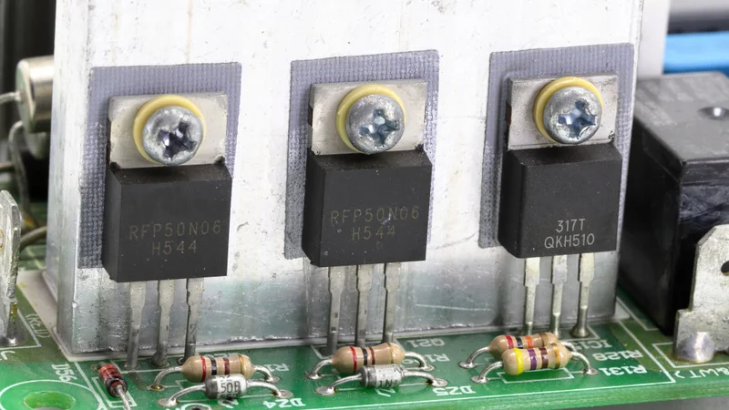
IGBTs mounted on a heat sink in a power supply circuit
Key Takeaways
An IGBT transistor, or insulated gate bipolar transistor, is best understood as a hybrid device: MOSFET-like insulated gate control driving a BJT-like bipolar conduction path.
The vertical IGBT structure uses a four-layer p-n-p-n stack, a MOS channel under a silicon dioxide gate, an n- drift region, and a p+ collector that injects minority carriers for conductivity modulation.
In many silicon IGBTs, practical gate drive is around +15 V VGE for turn-on and 0 V, -5 V, -10 V, or -15 V for turn-off, provided the gate-emitter maximum rating is not exceeded. A common maximum is ±20 V, although some devices specify other limits.
Compared with a high-voltage power MOSFET, an IGBT usually has lower on-state voltage at high voltage and high collector current, but slower turn-off because of stored charge and minority-carrier tail current.
The most important transistor-level limits are VGE maximum, VCE rating, collector current, power dissipation, switching loss, safe operating area, short-circuit withstand time, latch-up immunity, leakage current, ESD robustness, and thermal impedance.
IGBT modules and discrete IGBTs are often paired with freewheeling diodes in switching legs, but system applications such as motor drives, uninterruptible power supply hardware, solar inverters, and electric vehicles are secondary to the device physics covered here.
Introduction
The IGBT is short for insulated gate bipolar transistor. It is one of the defining power semiconductor devices in medium- and high-voltage power electronics. It combines a high input impedance, voltage-controlled gate terminal similar to a MOSFET, with a conductivity-modulated bipolar output structure closer to a BJT. That hybrid nature is the reason the IGBT transistor is often summarized as "MOSFET input, bipolar output."
This article focuses on the device itself: how the IGBT is built, how it conducts collector current, why its forward voltage drop differs from a power MOSFET, why turn-off produces tail current, and which transistor-level limits dominate engineering decisions. It focuses on IGBT applications such as motor drives, variable-frequency drives, uninterruptible power supply converters, switch-mode power supplies, solar inverters, induction heating, electric cars, and other electric vehicles in more depth.
At the standards level, IEC 60747-9:2019 defines terminology, letter symbols, essential ratings, characteristics, verification methods, and measurement methods for discrete insulated-gate bipolar transistors.
What an IGBT Transistor Is
An IGBT transistor is a three-terminal power semiconductor device with gate, collector, and emitter terminals. In an n-channel IGBT, which is the usual case for power switching, the gate controls an inversion channel in a p-body region. That MOS channel allows electron flow from the n+ emitter into the n- drift region, which in turn biases a p+ collector to inject holes into the drift region. The result is a bipolar conduction path controlled by an insulated MOS gate.
How IGBTs are Different from MOSFET and BJTs
A MOSFET conducts primarily through majority carriers. That gives power MOSFETs very fast switching and no minority-carrier tail current. However, in high-voltage MOSFETs the drift region resistance rises strongly as blocking voltage increases. At several hundred volts and above, that drift resistance can dominate on-state loss.
On the other hand, a BJT uses minority-carrier injection and can achieve high current density with low conduction voltage, but it needs base current drive and has charge-storage effects.
The IGBT borrows the BJT-like advantage of conductivity modulation while retaining MOS-gate voltage control. Infineon's IGBT characteristic material describes the equivalent device as a PNP transistor driven by an n-channel MOSFET, with minority-carrier injection from the p+ collector causing conductivity modulation in the n-region.

Internal Structure: MOS Gate Plus Four-Layer Bipolar Stack
The most common silicon IGBT is a vertical device. Current flows vertically from collector to emitter through a lightly doped drift region that supports high blocking voltage. A simplified n-channel IGBT cross-section contains these regions:
Region | Device function |
Gate electrode | Controls the MOS channel through an insulated gate structure |
Silicon dioxide gate insulation | Provides high input impedance and separates the gate terminal from the semiconductor |
n+ emitter | Provides electron injection into the MOS channel |
p-body or p-base | Hosts the inversion channel and forms part of the parasitic thyristor structure |
n- drift region | Supports collector-emitter blocking voltage and becomes conductivity-modulated in the on state |
Buffer or field-stop layer | Shapes the electric field and helps control switching and tail current in many modern devices |
p+ collector | Injects holes into the drift region, creating the bipolar conduction mechanism |
The layer sequence creates a p-n-p-n structure. That is essential to the IGBT's benefit and to one of its hazards. The p+ collector, n- drift region, p-body, and n+ emitter resemble a thyristor path. Internally, this can be represented as a parasitic PNP transistor coupled with a parasitic NPN transistor. If that parasitic thyristor regeneratively turns on, the device can enter latch-up, meaning the gate can no longer turn the device off normally.
Modern IGBTs are not all identical internally. Important structural variants include planar gate and trench gate cells, punch-through and non-punch-through structures, and field-stop devices. Trench gates improve channel density and reduce channel resistance. Field-stop layers shape the electric field so that the drift region can be thinner for a given voltage rating, which reduces conduction and switching losses.
The crucial structure-to-performance link is the n- drift region. In a high-voltage power MOSFET, the drift region remains a majority-carrier resistor. In an IGBT, the p+ collector injects holes during conduction. Those holes increase carrier concentration in the drift region, reducing its effective resistance.
This is conductivity modulation, and it is the physical reason an IGBT can have a lower on-state voltage than a high-voltage MOSFET at comparable voltage and current.
Suggested Reading: IGBT: Insulated Gate Bipolar Transistor Guide
Operating States, VGE, Collector Current, and VCE(sat)
In the off state, the gate-emitter voltage, VGE or Vge, is below threshold, so no inversion channel connects the n+ emitter to the drift region. The collector-emitter voltage is then supported mainly by the reverse-biased junction and the n- drift region. A real device still has leakage current, often specified as collector cut-off current or ICES.
In the on state, the gate terminal is driven positive with respect to the emitter. A channel forms in the p-body, electrons flow from the emitter side into the drift region, and the p+ collector injects holes. The IGBT's collector current is then carried by both electrons and holes, not just majority carriers. The resulting conductivity modulation lowers the on-state voltage drop across the drift region.
For high-power IGBT modules, a negative off-state gate voltage is common because it improves noise immunity against dv/dt-induced Miller turn-on. Mitsubishi's module application note recommends about +15 V ±10% for turn-on and a negative gate voltage such as -5 V to -10 V for turn-off in typical module drive conditions. In some designs, particularly noisy half-bridge environments, -15 V turn-off is used when the datasheet and gate driver allow it. The final limit is always the device's gate-emitter maximum rating.
The gate-emitter maximum rating varies by part. A common value is ±20 V. For example, Infineon's 600 V IKW40N60H3 lists a gate-emitter voltage rating of ±20 V, along with device-level ratings such as collector current, pulse current, power dissipation, turn-off safe operating area, and short-circuit withstand time.
The on-state voltage is specified as VCE(sat), the collector-emitter saturation voltage at a defined collector current, gate voltage, and junction temperature. Infineon's datasheet explanation states that VCE(sat) is typically specified at VGE = 15 V and several junction temperatures.
Device parameter | Typical engineering interpretation | Notes |
VGE(on) | Often +15 V | Common datasheet test and recommended drive condition for silicon IGBTs |
VGE(off) | 0 V, or negative bias such as -5 V to -10 V | Negative bias improves dv/dt immunity in bridge circuits |
Gate-emitter maximum | Often ±20 V, but datasheet-specific | Some devices specify ±25 V or other limits |
VCE(sat) | Commonly around 1.5 V to 3 V at rated conditions | Must be read at the specified IC, VGE, and junction temperature |
Collector current | DC and pulsed ratings depend on case temperature and cooling | Current rating is not independent of thermal design |
Short-circuit withstand time | Often a few microseconds in modern fast devices | Requires fast desaturation or overcurrent protection |
Switching frequency | Common IGBT range is from low kHz to tens of kHz | High voltage and high current reduce practical frequency |
Switching Physics: Turn-On, Turn-Off, and Tail Current
An IGBT turns on like a MOS-gated device but conducts like a conductivity-modulated bipolar device. During turn-on, the gate driver charges the input capacitances. The gate voltage rises to threshold, the collector current begins to increase, and the collector-emitter voltage falls. During the Miller interval, energy is transferred as VCE collapses while current is already flowing. In a half-bridge, reverse recovery of the complementary freewheeling diode can add turn-on loss.
Although the gate has high input impedance at DC, it is not "free" to drive dynamically. The gate driver must source and sink charge every cycle. Driver loss scales with total gate charge, gate voltage swing, and switching frequency.
Turn-off is where the IGBT differs most sharply from a power MOSFET. When the gate voltage falls, the MOS channel is removed. However, the n- drift region still contains stored minority carriers from conductivity modulation. Those carriers must recombine or be swept out. The remaining collector current forms the familiar tail current, which extends turn-off time and increases switching loss. Infineon explains that minority carriers stored in the n-layer slow switching and that the current tail increases switching losses.
This is why an IGBT's switching frequency is usually lower than that of a comparable MOSFET, especially when the voltage is moderate, and switching speed dominates. ROHM summarizes the practical range by showing discrete IGBTs and IGBT modules commonly used from about 1 kHz to 50 or 60 kHz, with the applicable frequency falling as output power increases because switching losses rise.
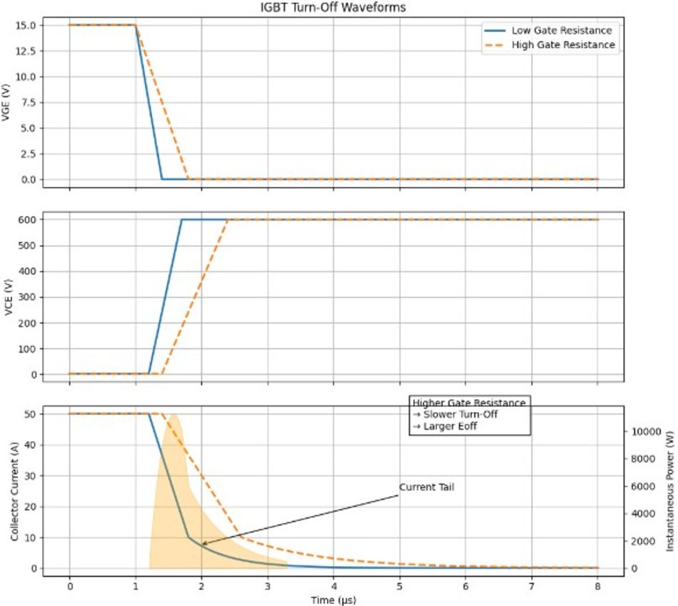
Power dissipation in an IGBT is the sum of conduction, switching, gate-drive, and leakage-related losses. A simplified engineering estimate is:
Ptotal ≈ Pcond + Psw + Pgate + Pleakage
For hard-switched operation:
Pcond ≈ VCE(sat) × IC × duty cycle
Psw ≈ fsw × (Eon + Eoff + Erec)
The actual calculation should use datasheet energy curves at the intended collector current, DC-link voltage, gate resistance, gate voltage, diode, and junction temperature. Thermal impedance, case temperature, package, heat sink, and layout then determine whether the calculated power dissipation is permissible.
IGBT vs MOSFET vs BJT at the Device Level
The IGBT, MOSFET, and BJT are often compared at the application level, but the deeper distinction is carrier physics and drive method.
Attribute | IGBT transistor | Power MOSFET | BJT |
Control terminal | Insulated gate terminal | Insulated gate terminal | Base-emitter junction |
Control type | Voltage-controlled | Voltage-controlled | Current-controlled |
Input impedance | High DC input impedance | High DC input impedance | Low to moderate, requires base current |
Main conduction physics | MOS channel drives bipolar conduction with minority-carrier injection | Majority-carrier channel and drift conduction | Bipolar minority-carrier injection |
On-state metric | VCE(sat) | RDS(on) | VCE(sat) |
High-voltage behavior | Conductivity modulation reduces drift-region loss | Drift-region resistance rises sharply with voltage rating | Low saturation voltage possible, but drive is harder |
Switching speed | Moderate, limited by stored charge and tail current | Fast, no minority-carrier tail | Slower than MOSFET, charge storage in saturation |
Reverse conduction | Usually needs diode or reverse-conducting structure | Intrinsic body diode exists | Not a bidirectional power switch by itself |
Gate or drive power | Low static gate power, dynamic gate-charge power | Low static gate power, dynamic gate-charge power | Continuous base drive power |
Failure concerns | Latch-up, tail current, SOA, short circuit, gate oxide, ESD | Avalanche, SOA, body diode recovery, gate oxide, ESD | Secondary breakdown, thermal runaway, drive overstress |
Best device-level fit | High voltage, high current, moderate switching frequency | Low to medium voltage or very high switching frequency | Linear and older power circuits where base drive is acceptable |
The MOSFET wins where switching speed, low gate charge, and absence of tail current dominate. This is common in low-voltage converters and high-frequency SMPS.
The IGBT wins where high blocking voltage and high collector current make the MOSFET's drift-region resistance too costly. At 600 V, 1200 V, and higher voltage classes, an IGBT can deliver lower conduction loss than an equivalent silicon MOSFET at comparable die size because of conductivity modulation.
The BJT is the historical reference point. It can offer bipolar conduction and high current density, but it needs a continuous base current and has harder drive requirements. The IGBT retained the bipolar output advantage while replacing base current drive with an insulated MOS gate. Silicon
Suggested Reading: Why IGBTs Remain Relevant in the Era of SiC and GaN Power Devices?
Safe Operating Area, Short Circuit, Latch-Up, Leakage, and ESD
An IGBT's safe operating area, or SOA, defines the voltage and current combinations over which the device can operate without damage under specified thermal and timing conditions. Toshiba describes SOA curves as showing allowable collector-emitter voltage and collector current regions, with separate forward-bias SOA and reverse-bias SOA considerations.
The RBSOA matters because turn-off can create collector-emitter voltage overshoot from stray inductance while collector current is still flowing. Toshiba defines RBSOA as the range in which the IGBT can be turned off without self-damage and notes that a surge voltage is generated by stray inductance during turn-off.
Short-Circuit Behavior
Short-circuit behavior is also specific to IGBTs. When a short occurs while the gate is driven on, collector current can rise to a desaturation current determined by device transconductance, VGE, junction temperature, and DC-link voltage. The device must survive until the gate driver detects the fault and turns it off safely.
Latch-up
Latch-up is the classic IGBT structural failure mode. The p-n-p-n stack contains a parasitic thyristor. If internal voltage drops and carrier injection biases the parasitic NPN and PNP pair regeneratively, the IGBT can remain on even if the MOS gate is turned off. Modern cell designs reduce latch-up susceptibility through p-body engineering, emitter shorts, lifetime control, and cell geometry, but latch-up remains a device concept every IGBT engineer should understand.
Gate oxide overstress is another major limit. Because the gate is insulated by silicon dioxide, it has high input impedance but finite oxide strength. Infineon's datasheet states that VGE is the maximum gate-to-emitter voltage, and that exceeding it can cause immediate failure or long-term oxide degradation.
Leakage Current
Leakage current matters both electrically and thermally. Collector leakage rises with temperature, and if the device is already hot, leakage-related heating can add to a positive thermal feedback path.
Recommended Reading: Gate Driver Design for Modern Power Electronics
Packaging, Diodes, and the Boundary Between Device and System
The transistor-level IGBT is only one part of the usable power switch. Devices are sold as discrete IGBTs, co-packaged IGBTs with diodes, reverse-conducting IGBTs, and multi-chip IGBT modules.
Modules may contain half-bridges, six-packs, choppers, or custom topologies with multiple IGBT chips, freewheeling diodes, thermistors, isolated baseplates, low-inductance terminals, and auxiliary emitter connections.
A conventional IGBT does not behave like a power MOSFET with a built-in body diode. Infineon notes that the reverse conduction characteristic of an IGBT is undefined in the way a MOSFET's intrinsic body diode is not. Therefore, switching legs usually pair IGBTs with freewheeling diodes.
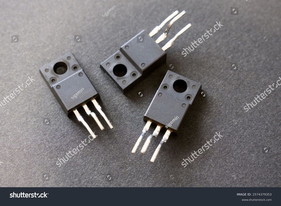
Some devices integrate a diode in the same package, and reverse-conducting IGBTs integrate reverse conduction monolithically. Toshiba's GT30J65MRB is one such example, described as an RC-IGBT with a monolithically integrated freewheeling diode.
Packages affect real transistor behavior. Bond-wire inductance, emitter inductance, thermal resistance, chip area, current density, and case-to-heat-sink interface all influence switching waveforms and reliability.
At high collector current, even a few nanohenries of stray inductance can produce significant voltage overshoot during di/dt. A Kelvin emitter terminal lets the gate driver sense emitter potential without sharing the main power emitter inductance, improving gate voltage control.
Reading an IGBT Datasheet Like a Device Engineer
A useful IGBT datasheet review starts with ratings, but it should not stop there.
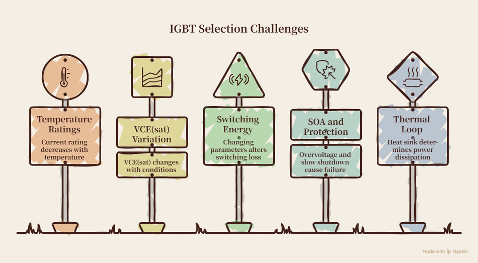
First, confirm the blocking voltage and collector current ratings at the real case temperature. A headline current rating at 25°C case temperature may be much higher than the continuous current at 100°C. Then check VGE maximum, because gate-driver supply tolerances, ringing, Miller spikes, and negative bias must fit inside that absolute maximum.
Second, inspect VCE(sat) curves rather than relying on a single typical value. VCE(sat) varies with collector current, junction temperature, and gate voltage. Some IGBTs have a positive temperature coefficient at higher current, which helps current sharing in modules, but their behavior at low current can be different.
Third, evaluate switching energy curves. Eon and Eoff are usually specified at defined VCE, IC, RG, VGE, diode, and junction temperature. Changing gate resistance, adding negative turn-off bias, changing diode technology, or operating at a different bus voltage can materially change switching loss. Infineon's device datasheets, for example, provide switching energy curves against collector current, gate resistance, junction temperature, and collector-emitter voltage under specified VGE conditions.
Fourth, verify SOA and short-circuit protection. A part that meets conduction and switching loss targets can still fail if turn-off overvoltage exceeds RBSOA, if short-circuit shutdown is too slow, or if gate drive causes excessive desaturation current. This is where transistor physics, package parasitics, and gate-driver design meet.
Finally, close the thermal loop. Compute conduction and switching losses, map them through transient thermal impedance or steady-state thermal resistance, and check junction temperature under worst-case operating conditions. Heat sink selection is not separate from the transistor. It determines whether the specified power dissipation can actually be removed.
Conclusion
The IGBT transistor is a deliberately hybrid power device. Its insulated MOS gate provides high input impedance and voltage-controlled drive, while its bipolar conduction path delivers conductivity modulation, high current density, and relatively low forward voltage drop at high blocking voltage. That combination explains why IGBTs remain central to power electronics even as power MOSFETs and SiC MOSFETs continue to improve.
The same physics also explains the limitations. The p-n-p-n structure introduces latch-up concerns, the silicon dioxide gate imposes VGE and ESD constraints, the conductivity-modulated drift region creates stored charge and tail current, and the switching waveforms must stay inside safe operating area. A good IGBT design is therefore not just a schematic symbol choice. It is a coordinated decision across device structure, gate voltage, collector current, VCE(sat), switching frequency, heat sinking, package parasitics, and fault handling.
FAQ
1. What is an IGBT transistor?
An IGBT transistor is an insulated gate bipolar transistor: a power semiconductor with a MOSFET-like gate and a BJT-like conduction path. The gate terminal is insulated, usually by silicon dioxide, so it has high DC input impedance and is driven by voltage rather than continuous current. Internally, the MOS channel controls bipolar conduction through a conductivity-modulated drift region. This gives the IGBT lower conduction loss than many high-voltage MOSFETs at high current, but slower turn-off because stored minority carriers must be removed.
2. How is an IGBT different from a MOSFET?
A power MOSFET is a majority-carrier device, so it can switch very fast and has no minority-carrier tail current. Its on-state loss is usually represented by RDS(on). An IGBT uses MOS gate control but conducts with bipolar carrier injection, so its on-state loss is represented by VCE(sat). At high voltage, conductivity modulation can make the IGBT more efficient in conduction than a silicon MOSFET, but the IGBT usually has higher turn-off switching loss and lower practical switching frequency.
3. How is an IGBT different from a BJT?
A BJT is current-driven through its base and needs a continuous base current to stay on. An IGBT is voltage-driven through an insulated gate, so its static input current is very low. Both use bipolar conduction physics, but the IGBT replaces base drive with a MOS-controlled channel. This is why the IGBT can provide BJT-like current density and conduction behavior while being easier to drive from a gate-driver IC. Toshiba notes that IGBTs require lower gate-drive power than BJTs because they are voltage-controlled devices.
4. What gate voltage should be used for an IGBT?
For many silicon IGBTs, the standard turn-on gate voltage is about +15 V VGE. Turn-off may use 0 V or a negative bias such as -5 V or -10 V to improve immunity against Miller-induced false turn-on. Some designs use -15 V if the device and driver ratings permit it. The gate-emitter maximum must never be exceeded. A common limit is ±20 V, but some devices specify different values, so the selected datasheet is authoritative.
5. What is VCE(sat) in an IGBT?
VCE(sat) is the collector-emitter saturation voltage when the IGBT is on at a specified collector current, gate voltage, and junction temperature. It is the closest IGBT equivalent to a MOSFET's on-resistance figure, although it is not a resistance. Lower VCE(sat) reduces conduction loss, approximately VCE(sat) × IC × duty cycle. Datasheets commonly specify VCE(sat) at VGE = 15 V, but values change with current and temperature, so curves are more useful than a typical number.
6. Why does an IGBT have tail current?
Tail current occurs because the IGBT's n- drift region is filled with stored minority carriers during conduction. When the gate turns off, the MOS channel disappears quickly, but those stored carriers must recombine or be extracted before collector current fully stops. That residual current creates turn-off loss, increases Eoff, and limits switching frequency compared with a MOSFET. Tail current is not a packaging artifact. It is a direct consequence of conductivity modulation, which is also the mechanism that gives the IGBT its low on-state voltage.
References
Toshiba Electronic Devices & Storage, IGBTs: Insulated Gate Bipolar Transistor Application Note
Infineon Technologies, IGBT Characteristics, AN-983
Infineon Technologies, Discrete IGBT Datasheet Explanation
Mitsubishi Electric, IGBT Module Application Note
ROHM Semiconductor, New Gen3 650V IGBT Application Note
in this article
1. Introduction2. What an IGBT Transistor Is3. Internal Structure: MOS Gate Plus Four-Layer Bipolar Stack4. Operating States, VGE, Collector Current, and VCE(sat)5. Switching Physics: Turn-On, Turn-Off, and Tail Current6. IGBT vs MOSFET vs BJT at the Device Level7. Safe Operating Area, Short Circuit, Latch-Up, Leakage, and ESD8. Packaging, Diodes, and the Boundary Between Device and System9. Reading an IGBT Datasheet Like a Device Engineer10. Conclusion11. FAQ12. References