Comprehensive Guide to 4-bit Adders: Theory, Implementation and Modern Innovations
Arithmetic units are a core element in digital systems. But their design is not as simple as it may seem. This article explores the theory behind 4 bit adders and their comparison with various architectures. It will examine integrated circuits and discuss the modern low power research and designs.

14 Nov, 2025. 11 minutes read

Key takeaways
4-bit adders are the fundamental building blocks of digital systems, allowing the addition of two 4-bit binary numbers. The configuration features four cascaded full-adders with a carry input and output.
Carry look-ahead adders are an innovative adder configuration designed to overcome the delay, as they can compute and generate carry simultaneously. They can add faster, but have more complex hardware.
Ripple carry adders are simple and cost-effective adders, where the carry bit ripples through each stage of the adder. These adders have a propagation delay as the last adder must wait for the carry bit from the previous stages to compute the final carry and sum.
4-bit adders are readily available in standard integrated circuits like 74LS83 and 74HC83. These packages provide fast carry logic and simplify hardware design.
Thanks to modern research, techniques like Gate Diffusion Input (GDI) and Multi-threshold transistors have contributed to lower power consumption and reduced area.
Introduction
Digital systems perform two fundamental operations, i.e., Arithmetic and logical. From simple microcontrollers to high-end processors, all digital systems require physical circuits, often called arithmetic units to execute mathematical instructions. At the core of these units lie adders. Adders are circuits that perform binary addition. While they are fundamental units that can add two single-bit numbers, a 4-bit adder remains a basic element that comprises individual adders. It’s a building block and fundamental element for teaching digital logic and for building larger arithmetic units, cascading or expanding bit widths. Understanding the operation of 4-bit adders is therefore essential for digital design engineers, hardware engineers, and electronics students.
This article discusses 4-bit adders in depth. We will discuss the fundamentals of binary addition, half and full adders, and how they combine into a 4-bit adder. The article then compares ripple carry and carry look-ahead architectures, using equations and block diagrams to illustrate how carries propagate. We will further look into practical implementation, such as using the 74LS83 integrated circuits. Moreover, find out some insights on the recent research on energy-efficient designs, including Gate Diffusion Input (GDI) and other low-power techniques, and discuss design considerations and future trends.
Suggested Reading: Microprocessor vs Integrated Circuit: Unveiling the Core of Modern Technology
Basics of Binary Addition
Binary Representation
Computers use base-2 representation. For executing instructions, computers convert instructions to binary values, also called machine code. The machine codes consist of bits that take the value 0 or 1.
A 4-bit number can represent values from 0 (0000₂) to 15 (1111₂). When two binary numbers are added, bit values and carry bits must be considered.
Half Adder and Full Adder
Adder circuits are mainly of two types, i.e., Half Adder and Full Adder. They primarily differ in the way they deal with the carry input.
Half Adder Circuit
A half adder adds two single bits (A and B) and produces a sum (S) and a carry bit (C ), given by the following formulae.

It is the simplest adder circuit that has two inputs and two outputs. However, it cannot handle an incoming carry bit.
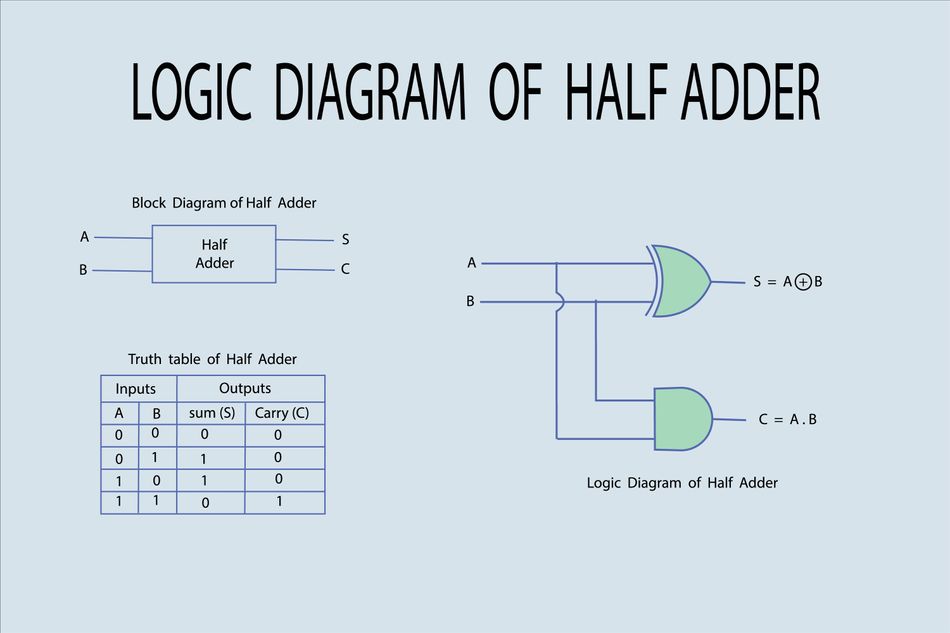
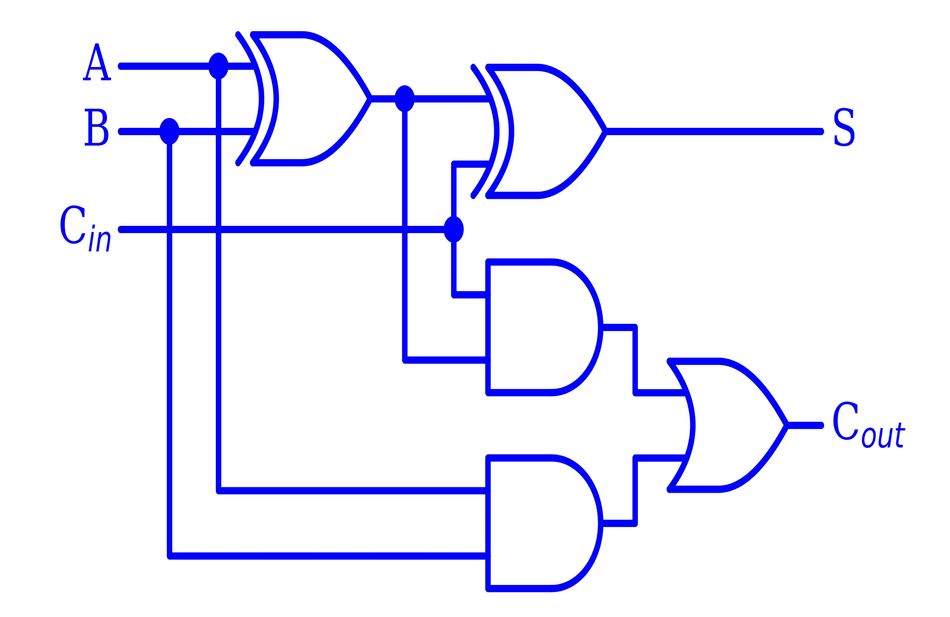
Full Adder Circuit
A full adder extends the functionality of a half adder by including a carry input Cin. So, it adds three bits (A, B, and Cin) to produce a sum and a carry output (Cout). The full adder equations are:

The following table summarizes the characteristics of half and full adders.
Adder type | Inputs | Carry input | Outputs | Carry handling | Complexity | Applications |
Half adder | Two bits (A, B) | No | Sum, carry | No incoming carry; only produces carry | Simple | Basic addition, parity circuits |
Full adder | Three bits (A, B, Cin) | Yes | Sum, carry | Handles incoming carry and produces carry | More complex | Used in cascaded adders and arithmetic units |
A 4-bit adder is created by cascading four full adders. Each full adder computes one bit of the sum and passes a carry to the next stage.
4-bit Ripple Carry Adder
A ripple carry adder connects full adders in sequence. It adds two 4-bit numbers A (A0 - A3) and B (B0 - B3). The carry output of the first adder becomes the carry input of the second adder and the sequence continues. As a result, the adder circuit produces the sum bits S0 through S3 and carry out C4. It is important to note that the carry input of the first adder is set to 0.
The carry bit ripples through each full adder, and therefore it’s called a Ripple Carry Adder. The following figure illustrates the operation of a 4-bit adder:
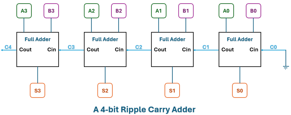
In a ripple carry adder, each full adder i computes:

As mentioned earlier, the carry bit must ripple through all stages. For example, if the adder must compute S3 and C4, it must wait for carry bits from stage 0 till stage 2. So, it induces a serial dependency, called propagation delay.
For example, the first full adder must compute its output before the fourth adder receives a valid carry. Hence, if each stage has a 20 ns delay, the sum bit S3 will be valid after roughly 60 ns. And the overall 4-bit sum appears after accumulating delays from all stages.
Propagation Delay and Limitations
The ripple carry architecture is conceptually simple and economical because it requires just four full adders. But the sequential propagation of the carry leads to significant delays, especially when the bit widths increase. This propagation delay is the sum of the delays of each full adder.
So, an n-bit ripple carry adder experiences delay proportional to n. It may be acceptable for a 4-bit adder, but larger word sizes (8, 16, 32 bits) can produce considerable latency, especially in high-performance processors.
Even with the drawback, ripple carry adders remain popular because they are inexpensive to implement and require fewer logic gates than more sophisticated architectures. They are often used where speed is less critical, such as in microcontrollers, small ALUs or simple digital logic courses.
Suggested Reading: Microcontroller vs Microprocessor: A Comprehensive Guide to Their Differences and Applications
Advantages and disadvantages
Aspect | Advantages | Disadvantages |
Hardware cost | Minimal hardware; uses one full adder per bit | None |
Complexity | Simple structure and easy to design | None |
Speed | Slow; carry must ripple through all stages | Propagation delay grows linearly with bit width |
Scalability | Easily scaled by adding more full adders | Delay increases; unsuitable for high-performance units |
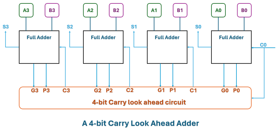
Carry Look-Ahead Adders
Ripple carry adders generate propagation delays as word sizes grow, eventually reaching a point where they become unacceptable. To improve speed, engineers developed carry look-ahead adders (CLAs).
The key idea is to calculate carry bits in advance based on the inputs. So, the full adder, regardless of its position, computes the sum, instead of waiting for carries to ripple. This is achieved by defining propagate (P) and generate (G) signals for each bit position:

A generate signal (G) means that a carry will be produced at that bit irrespective of the input carry.
A propagate signal (P) indicates that if a carry comes into the bit, it will propagate to the next stage.
Using these signals, the carry at bit i+1 can be computed by:

How Does the 4-bit CLA Logic Work?
In a 4-bit CLA, carries C1–C4 are calculated using P and G terms and the initial carry C0. For example, the first few carry bits are:
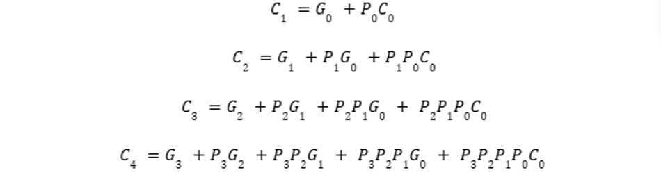
The formulas indicate that carry bits can be derived from the propagate and generate signals without sequential dependency.
Once carries are determined, the sum bits are calculated as:

Since carry bits are computed in parallel, it reduces the propagation delay significantly. Hence, it’s much faster than ripple carry adders.
Advantages and Trade-offs
The major advantage of carry look-ahead adders is speed. Because carries are computed in parallel using P and G signals, the overall delay is significantly lower than a ripple carry adder—especially noticeable with wider bit widths.
But this improvement comes at the cost of increased hardware complexity and gate count, particularly in the look-ahead logic. The arithmetic unit must implement multiple levels of logic to compute the generate and propagate terms and combine them appropriately.
As a result, CLAs consume more power and silicon area compared with ripple carry adders.
Suggested Reading: Silicon Wafers: Production, Properties and Application
Implementation of 4-Bit Adders with Standard ICs
74LS83 and 74HC83 4-bit adders
Modern integrated circuits contain 32-bit or 64-bit adders, but discrete 4-bit adder chips are still valuable for education and prototyping. The 74LS83 and 74HC83 are classic TTL/CMOS devices that implement a 4-bit binary full adder with fast carry capability.
They add two 4-bit numbers A0–A3 and B0–B3, accept a carry input Cin and produce sum outputs S0–S3 and a carry out Cout.
Electrical Characteristics
The 74HC83 is a CMOS variant that operates from 2–6 V and drives up to ±4 mA output current, making it suitable for low-power applications. The 74LS83 is a TTL variant that requires a 5 V supply and can sink more current but sources only a few milliamps.
Both chips implement fast carry look-ahead across four bits, providing quick addition. According to the manufacturer, these devices are standard 4-bit binary full adders with full carry look-ahead and fast add times.
Modern research and energy-efficient designs
Gate Diffusion Input (GDI) full adders
Power efficiency and area reduction are critical in battery-powered devices and high-density integrated circuits. Gate Diffusion Input (GDI) technology offers a technique for building logic gates and adders with fewer transistors than conventional CMOS.
A 2025 research study compared full swing GDI-based adders with hybrid designs and reported 14.8 % power savings and 55 % area reduction in a 4-bit full adder. The same work noted that GDI-based arithmetic circuits achieved more than 41 % improvement in delay and 32 % reduction in energy consumption compared with standard CMOS full adders.
Researchers have also combined GDI with multi-threshold (MVT) transistors, resulting in hybrid architectures that improved energy savings by over 57 % and reduced the energy–delay product (EDP) by 92 %. These techniques reduce leakage currents and allow for adjustable trade-offs between speed and power.
Suggested Reading: Transistor as a Switch: Theory and Practical Implementation for Digital and Hardware Engineers
Performance of Conventional CMOS adders
To appreciate these improvements, consider that a conventional 1.8 V CMOS full adder with 28 transistors consumes between 1084 and 1217 nW of power and exhibits 22.6–31.8 ps propagation delay.
GDI and hybrid architectures significantly reduce both power and delay compared to these baseline values.
Fabrication Challenges and design trade-offs
The adoption of GDI and hybrid logic is not without challenges. Implementing GDI logic often requires twin-well or silicon-on-insulator (SOI) processes. Researchers note that these processes complicate fabrication and may impact yield.
Other Architectural Innovations
There are several notable architectures that are deployed in modern processors. Here is a quick look
Carry-select adders divide inputs into segments and precompute sums assuming different incoming carries. They choose the correct sum once the actual carry arrives.
Carry-skip (bypass) adders allow a carry to skip over certain groups of bits using propagate conditions, reducing delay.
Parallel prefix adders (e.g., Kogge–Stone, Brent–Kung) use a tree structure to compute carries in logarithmic time, offering high performance at the cost of complex interconnect.
Quantum Dot Cellular Automata (QCA) and memristor-based adders represent emerging technologies exploring nanoscale implementations and non-CMOS devices. These are still research topics and are beyond the scope of this guide.
These families are primarily used for wider byte sizes. However, the selection of an adder architecture depends on application requirements such as speed, area, power, and ease of implementation. For small bit widths or teaching purposes, ripple carry and carry look-ahead adders remain dominant choices.
Practical design considerations
Design Flow and Simulation
When designing a 4-bit adder in hardware description languages such as Verilog or VHDL, follow these steps:
Define modules for half adder and full adder with clear port names (A, B, C_in, S, Cout).
Instantiate four full adders in a top-level module. Connect A and B inputs to the appropriate bit slices and route Cout from each adder to Cin of the next.
Add carry look-ahead logic if implementing a CLA. Compute the propagate and generate signals and derive C1–C4 according to the equations given earlier.
Simulate the design using a testbench. Apply exhaustive or representative input vectors and verify that sums and carries are correct. For a 4-bit adder, there are 2^9 (512) possible combinations of A, B, and Cin.
Synthesize and implement the design on target hardware (FPGA or ASIC). Use timing analysis to ensure that the critical path meets performance requirements. For ripple carry adders, the critical path includes all full adder delays; for CLAs, the look-ahead logic may dominate.
Using off-the-shelf ICs
When building a physical circuit with a 74LS83/74HC83:
Power supply: Provide stable 5 V for LS devices or 2–6 V for HC devices. Use decoupling capacitors to reduce noise.
Input connections: Connect A and B lines to DIP switches or microcontroller outputs. Tie unused inputs to a defined logic level to prevent floating.
Carry handling: If cascading two 74LS83 chips to create an 8-bit adder, connect the carry out of the lower nibble to the carry in of the higher nibble. Use the fast carry pins where available.
Testing: Use LEDs or logic analyzers to observe sum outputs and verify correct operation across all input combinations.
Conclusion
A 4-bit adder is a fundamental yet instructive circuit. The ripple carry adder demonstrates how full adders can be cascaded. However, it suffers from a propagation delay proportional to bit width. Carry look-ahead adders can handle this delay by generating carries in parallel using propagate and generate signals. Each architecture presents trade-offs between simplicity, speed, and hardware cost. Off-the-shelf ICs such as the 74LS83 and 74HC83 provide convenient 4-bit adder implementations with fast carry logic.
Modern research shows that energy-efficient designs using Gate Diffusion Input and hybrid logic can achieve significant power and area savings—up to 55 % area reduction and notable improvements in delay. Future work continues to explore novel architectures such as parallel prefix adders, asynchronous adders, quantum dots, and memristor-based implementations.
FAQs
1. What is a 4-bit adder?
A 4-bit adder is a digital circuit that adds two 4-bit binary numbers. It outputs a 4-bit sum and a carryout bit. By cascading four full adders, each handling one bit, the circuit performs addition across all bits. The carry output of each stage feeds the next stage, allowing the adder to handle numbers up to 15 (decimal).
2. How does a ripple carry adder differ from a carry look-ahead adder?
A ripple carry adder passes the carry from one full adder to the next sequentially. The last stage cannot output its result until all previous carries have propagated. In contrast, a carry look-ahead adder computes propagate and generate signals and derives carries simultaneously. This parallel computation greatly reduces delay but requires more logic.
3. What are the advantages of using a 74LS83/74HC83 chip?
These ICs offer a ready-made 4-bit full adder with fast carry look-ahead. They simplify circuit design by providing predefined pinouts and built-in carry logic. The 74HC83 operates at a wide voltage range and low power, while the 74LS83 is optimized for TTL compatibility.
4. How is overflow detected in a 4-bit adder?
Overflow occurs in signed arithmetic when the result exceeds the representable range. For a two's complement 4-bit adder, compare the carry into the most significant bit (C3) with the carry out (C4). If they differ, overflow has occurred. Some ICs provide an overflow flag; otherwise, you can derive it with additional logic.
5. What modern techniques reduce power in adder designs?
Techniques such as Gate Diffusion Input (GDI) and multi-threshold transistor logic reduce transistor count and lower dynamic and static power consumption. Research reports power savings of 14.8 % and area reduction of 55 % using GDI full adders, and energy-delay product improvements of over 92 % with hybrid GDI/MVT designs.
5. Can I cascade 4-bit adders to create larger adders?
Yes. You can connect the carry out of a 4-bit adder to the carry in of another 4-bit adder to create an 8-bit, 12-bit, or larger adder. For ripple carry adders, the carry will propagate through each stage; for ICs like 74LS83, use the fast carry pins to minimize delay.
6. What are other adder architectures beyond ripple and carry look-ahead?
Other architectures include carry-select adders, carry-skip adders, parallel prefix adders (e.g., Kogge–Stone, Brent–Kung), and emerging technologies like quantum dot cellular automata and memristor-based adders. Each offers a different balance of speed, power and complexity.
References
Electrical Technology, "Ripple Carry And Carry Look Ahead Adder – Logic & Block Diagrams," Apr. 2018. [Online]. Available: https://www.electricaltechnology.org/2018/04/ripple-carry-and-carry-look-ahead-adder.html
GeeksforGeeks, "Carry Look Ahead Adder," Mar. 2024. [Online]. Available:https://www.geeksforgeeks.org/digital-logic/carry-look-ahead-adder/
Microcontrollers Lab, "74LS83 4 Bit Full Adder Pinout, Examples, Applications, Datasheet," [Online]. Available: https://microcontrollerslab.com/74ls83-4-bit-full-adder-pinout-examples-applications-datasheet/
Build Electronic Circuits, "74HC83 and 74LS83 4-bit Binary Adder IC," [Online]. Available: https://www.build-electronic-circuits.com/7400-series-integrated-circuits/74hc83-74ls83/
Mohamad Zarith et al., "Special Issue IJIRM Vol. 13-S March 2025: GDI Technique for Low Power Digital Design," KLUST, 2025. [Online]. Available: https://klust.edu.my/pdf/2-special-issue-ijirm-vol-13-s-march-2025-mohamad-zarith.pdf
Futurlec, "74LS83 4 Bit Binary Full Adder," [Online]. Available: https://www.futurlec.com/74LS/74LS83pr.shtml