GDDR6 vs GDDR6X: A Comprehensive Technical Comparison for Digital Design & Hardware Engineers
Discover key differences in GDDR6 vs GDDR6X memory: compare bandwidth, power efficiency, signaling methods, and design trade-offs for advanced GPU architectures.

06 Oct, 2025. 18 minutes read
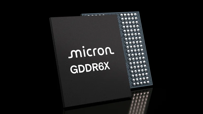
GDDR6X by Micron
Introduction
The debate of GDDR6 vs GDDR6X has become crucial as modern GPUs demand high speed and efficiency. Both memory standards underpin next-generation gaming, visualization, and AI workloads. For digital design engineers, understanding GDDR6 vs GDDR6X goes beyond bandwidth figures—it involves analyzing power efficiency, signaling schemes, and PCB routing constraints. While both standards build on the lessons of GDDR5X, their signaling methods, power characteristics, and system requirements differ markedly.
GDDR6, standardized by JEDEC and introduced in 2017, extended GDDR5X by increasing per‑pin speeds to 16 Gb/s, introducing a dual‑channel architecture, and lowering operating voltage. Micron and Nvidia later collaborated to develop GDDR6X, an evolutionary step that replaces NRZ signaling with PAM4, doubling the data throughput per symbol.
This article provides a systematic comparison of GDDR6 vs GDDR6X to help hardware architects choose the optimal memory interface for power-sensitive, high-bandwidth systems!
Evolution of GDDR and the Rise of GDDR6X
From GDDR5X to GDDR6
The evolution of GDDR memory has been shaped by the growing performance needs of graphics cards, GPUs, and AI workloads. Derived from traditional DDR SDRAM, it diverged early to prioritize high bandwidth over low latency, aligning better with parallel GPU architectures.
GDDR5, introduced in 2008, became the backbone of the gaming and workstation era, powering cards such as the GeForce GTX 900 series by Nvidia and Radeon RX 500 by AMD. However, its NRZ signaling and 8n prefetch limited scaling beyond 8 Gb/s per pin.
To extend the standard, GDDR5X was launched around 2016, co-developed by Micron and Nvidia, enabling data rates up to 14 Gb/s. [1] It increased prefetch length to 16n, improved I/O signaling, and introduced advanced clocking modes. Yet, as GPU compute and real-time rendering advanced, bandwidth bottlenecks became critical—particularly in ray tracing, AI training, and video editing workloads.
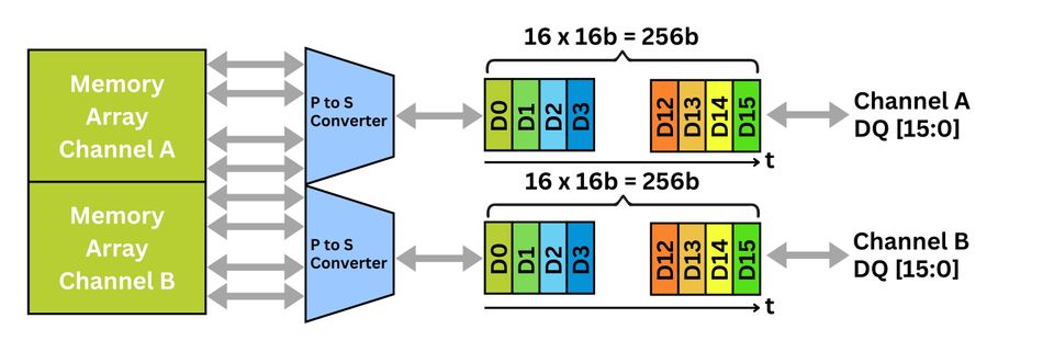
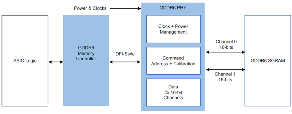
GDDR6, standardized by JEDEC in 2017, was a substantial leap forward. It split the 32-bit interface into two independent 16-bit channels, each with its own command, address, and data bus. This dual-channel architecture improved efficiency, allowing simultaneous transactions and better parallelism within the GPU memory controller.
Each channel performs a 16n prefetch, fetching 16 sequential 16-bit words internally per access. When serialized, the total transfer equals a 256-bit (32-byte) burst per operation, substantially improving memory bandwidth utilization.
GDDR6 memory also features on-die termination (ODT), training sequences, and error detection codes, thereby enhancing signal integrity and reliability during high-speed operation. The operating voltage (VDD) dropped to around 1.35V, significantly improving power efficiency compared to GDDR5X.
These architectural improvements enabled GDDR6 to reach 16 Gb/s per pin, allowing for 256-bit, 320-bit, and 384-bit memory buses across modern Nvidia RTX and AMD Radeon architectures.
The Need for Higher Bandwidth
Today, GPU cores are scaled into the tens of thousands, making memory bandwidth the dominant performance bottleneck. Each new generation of graphics processing units demanded faster data transfer rates to feed shader cores, RT units, and tensor accelerators.
For example, at 16 Gb/s per pin, a 384-bit GDDR6 bus provides around 768 GB/s of peak bandwidth (excluding protocol overhead). [2] High-end GPUs like Nvidia RTX 6000 Ada utilize 48 GB of GDDR6 to achieve nearly 960 GB/s, an impressive figure, but still constrained for AI inference or 8K rendering workloads.

In contrast, High Bandwidth Memory (HBM), a 3D-stacked DRAM solution, delivers multiple terabytes per second through ultra-wide interfaces. However, its cost, interposer packaging, and thermal design complexity restrict its adoption to datacenter GPUs and AI accelerators.
This growing gap created a need for a cost-effective alternative that can bridge mainstream GPUs and HPC workloads. The solution came with GDDR6X, developed jointly by Micron and Nvidia.
The Emergence of GDDR6X
Unveiled in 2020 with GeForce RTX 3080 and RTX 3090, GDDR6X memory marked the first industrial use of PAM4 signaling in a commercial GPU. Instead of traditional NRZ encoding, which transmits one bit per clock, PAM4 signaling uses four voltage levels to encode two bits per symbol, effectively doubling throughput without doubling clock speed.
This pulse amplitude modulation approach allowed data transfer rates of 19–21 Gb/s per pin, with advanced bins later reaching 24 Gb/s. When paired with a 384-bit memory bus, the theoretical bandwidth approaches 1 TB/s, rivaling some HBM2E solutions at a fraction of the cost and complexity.
Beyond signaling, GDDR6X integrates enhanced equalization, error correction, and power delivery optimizations to maintain signal integrity at these extreme clock speeds. It remains electrically compatible with GDDR6, allowing similar motherboard and PCB routing topologies, though design margins are tighter.
By striking a balance between high bandwidth and manufacturing cost, GDDR6X became the memory of choice for Nvidia RTX 30-series, RTX 40-series, and professional workstation GPUs. Its efficiency and scalability have made it pivotal in enabling real-time ray tracing, AI inference, and VR rendering at unprecedented frame rates.
Looking forward, GDDR6X represents the transitional phase toward GDDR7, which aims to combine higher bandwidth, lower power consumption, and improved PAM4 signaling efficiency.
Recommended Reading: HBM Memory: Complete Engineering Guide & Design Optimization 2025
Memory Architecture and Prefetching
Dual‑Channel Interface
Both GDDR6 and GDDR6X adopt a dual-channel interface, exposing two independent 16-bit channels per memory chip. Each channel features its own command/address, data, and bank group pins, enhancing signal integrity and parallelism.
The internal DRAM core is typically divided into 16 banks, arranged as eight per channel. Commands such as READ, WRITE, and ACTIVATE are distributed independently, allowing concurrent operations across multiple channels and banks. This interleaving minimizes idle cycles and sustains higher bandwidth under mixed GPU workloads.
By isolating channels, bus capacitance and command collisions are reduced, improving timing closure at 16 Gb/s and beyond. Such architecture also enables fine-grained scheduling, allowing graphics cards and AI accelerators to sustain consistent data delivery under real-time rendering and AI training conditions.
For Nvidia RTX and AMD Radeon GPUs, this dual-channel design improves memory utilization, especially in compute-intensive or ray-tracing pipelines, where simultaneous access to multiple bit buses minimizes latency.
16n Prefetch Architecture
The 16n prefetch is central to the efficiency of GDDR6 memory. It fetches 16 data words per I/O per access, optimizing data transfer rates while maintaining manageable core frequencies. [3]
Each channel in GDDR6 issues 32-byte bursts, computed as:
2 channels × 16 words × 2 bytes/word = 64 bytes per full device transaction
Because of 16n prefetching, the core frequency operates at one-sixteenth of the I/O data rate. For example, a 16 Gb/s external interface corresponds to a 1 GHz DRAM core, which reduces power consumption and eases timing constraints.
GDDR6X retains this prefetch depth but adjusts burst length to BL8, leveraging PAM4 signaling to double the bits transmitted per unit interval. Each channel still transfers 32 bytes per operation, but with higher symbol density, achieving up to 21 Gb/s per pin, and even 24 Gb/s in advanced variants.
This combination of 16n prefetch and PAM4 encoding provides nearly 1 TB/s of aggregate bandwidth on a 384-bit bus, approaching HBM2E-class performance without the need for complex 3D stacking. The trade-off is tighter signal margins, requiring careful PCB layout, termination, and controller timing calibration.
Bank Group Architecture
Within each GDDR6 and GDDR6X channel, the 16 banks are partitioned into bank groups to maximize parallel command execution. Each bank group can accept a command every core clock, enabling pipelined scheduling across active rows.
This bank group architecture mitigates row-to-row switching penalties, a common cause of latency bottlenecks in earlier GDDR5X designs. By alternating commands across groups, engineers can maintain continuous data flow and reduce read-write turnaround times.
For GPU memory controllers, intelligent bank interleaving algorithms distribute workloads to avoid conflicts, ensuring steady throughput and improved energy efficiency. This becomes vital when handling AI inference, high-frame-rate rendering, or real-time simulation tasks, where predictable memory access latency is essential.
Designers should align address mapping policies with bank group scheduling to ensure concurrent activation without violating timing constraints (tRRD, tFAW). Proper command distribution across bank groups significantly enhances effective bandwidth while preserving power efficiency under sustained load.
Recommended Reading: HBM2 vs GDDR6: Engineering Deep Dive into High-Performance Memory Technologies
Signaling and Encoding: NRZ vs PAM4
NRZ (PAM2) Signaling in GDDR6
Non-return-to-zero (NRZ), also called PAM2 signaling, has long been the foundation of GDDR memory interfaces. In this scheme, binary data is represented by two voltage levels, high for “1” and low for “0”. Each unit interval (UI) carries exactly one bit, keeping circuit design relatively simple and predictable.
In GDDR6, this method pushes performance nearly to its practical limit. At 16 Gb/s per pin, the UI window narrows to roughly 62.5 picoseconds, leaving minimal margin for jitter, crosstalk, or voltage droop. Maintaining signal integrity under such constraints requires precise equalization, on-die termination, and adaptive training algorithms.
To ensure error-free data transfer, GDDR6 memory employs cyclic redundancy check (CRC) and read/write strobes to align sampling edges. However, higher clock speeds and signal swings translate to greater I/O power consumption, reducing energy efficiency for GPUs and graphics cards operating at extreme bandwidths.
This is where traditional NRZ signaling reaches a scaling wall—further doubling data rate would require halving timing margins, making physical implementation increasingly expensive and thermally constrained.
PAM4 Signaling in GDDR6X
To overcome NRZ limitations, Micron and Nvidia introduced PAM4 signaling in GDDR6X memory, marking the first commercial use of multi-level modulation in GPU VRAM.
PAM4 (Pulse Amplitude Modulation 4) encodes two bits per symbol using four voltage levels—00, 01, 10, 11. [4] This doubles data throughput without increasing symbol frequency, thereby improving energy efficiency.
For instance, achieving 16 Gb/s effective bandwidth with NRZ requires a 16 GHz signaling rate, whereas PAM4 achieves the same throughput at only 8 GHz. This frequency reduction effectively doubles the timing window to ~125 ps, simplifying timing closure and reducing power per bit.
However, PAM4 signaling introduces new challenges! The receiver must discriminate between four distinct voltage thresholds, making it highly sensitive to noise, power-rail ripple, and inter-symbol interference. Micron redesigned the GDDR6X I/O path, adding three sub-receivers per line and implementing Data Bus Inversion (DBI) for noise mitigation.
While this architecture lowers symbol frequency, it increases receiver complexity, area, and cost, demanding clean reference voltages, robust PCB routing, and precise termination networks. Engineers must maintain open-eye diagrams across all four amplitude levels to preserve signal integrity at speeds of up to 24 Gb/s per pin.
The result is a balanced trade-off; GDDR6X achieves a near-1 TB/s aggregate memory bandwidth on a 384-bit bus, rivaling HBM2E performance while offering simpler packaging.
Encoding and Burst Length
Because PAM4 signaling transmits two bits per UI, GDDR6X halves its burst length (BL8) while maintaining 32 bytes per access, identical to GDDR6 (BL16). This adjustment preserves bus efficiency and simplifies controller scheduling. The simplified comparison is below:
| Feature | GDDR6 (NRZ) | GDDR6X (PAM4) |
| Signaling | NRZ (PAM2), 1 bit/UI | PAM4, 2 bits/UI |
Burst Length | 16 words (BL16), 32 bytes per channel | 8 words (BL8) but 2 bits/UI → 32 bytes per channel |
| Sub‑Receivers | 1 per I/O | 3 per I/O (to sample four levels) |
| Clock Frequency | High (e.g., 16 GHz) | Half (e.g., 8 GHz) |
| Training Complexity | Standard | More complex (requires additional training to align voltage levels) |
This comparison illustrates how PAM4 effectively reduces symbol frequency and improves energy per bit, yet demands complex equalization and advanced training algorithms. For digital design engineers, understanding these encoding trade-offs is essential when balancing bandwidth, power consumption, and reliability in modern GPU memory architectures.
Recommended Reading: Maximize GPU Utilization for Model Training: Unlocking Peak Performance
Bandwidth, Data Rates, and Capacity
Per‑Pin Speeds and System Bandwidth
The bandwidth advantage of GDDR6X over GDDR6 is one of its defining characteristics. GDDR6 memory operates at 14–16 Gb/s per pin, while GDDR6X achieves 19–21 Gb/s, with 24 Gb/s parts entering volume production in the coming years.
The system bandwidth scales linearly with bus width. For GPUs equipped with a 384-bit interface, typical aggregate values are:
| Memory | Typical Per‑Pin Rate | System Bandwidth (384‑bit bus) |
| GDDR5X | 11.4 Gb/s | ≈ 547 GB/s |
| GDDR6 | 14–16 Gb/s | ≈ 672–768 GB/s |
| GDDR6X | 19–21 Gb/s | ≈ 912–1008 GB/s |
| GDDR6X (24 Gb/s) | 24 Gb/s | ≈ 1.152 TB/s |
The above table shows that GDDR6X offers approximately 50% more bandwidth than GDDR6 at the same bus width. The extra headroom allows GPUs to sustain higher throughput for compute‑heavy tasks.
Capacity Per Device
GDDR6 devices are widely available in 4 GB to 32 GB capacities, offering flexibility across consumer, workstation, and AI GPU segments. The GDDR6X memory range currently spans 8 GB to 24 GB per chip, with larger densities under development.
Higher-capacity chips reduce the number of memory packages required on the graphics card PCB, simplifying routing and controller design. However, fewer packages also mean greater thermal concentration, requiring improved cooling solutions and power management strategies.
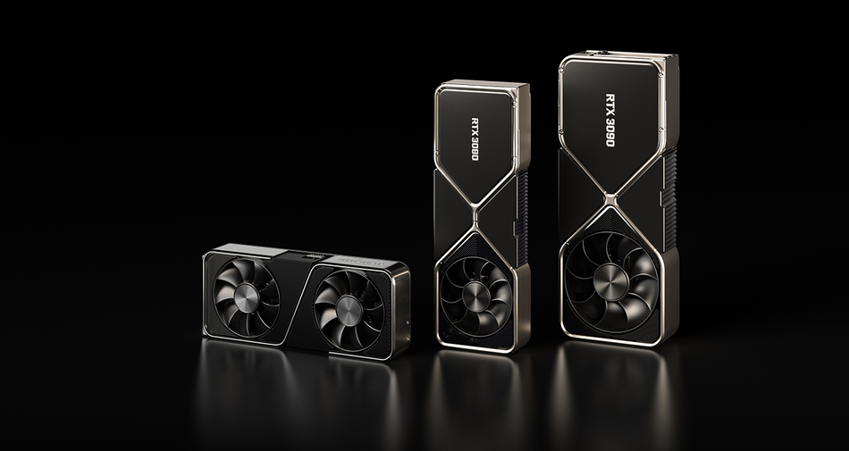
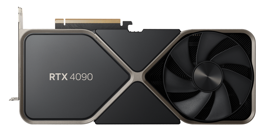
RTX 4090 by Nvidia, for instance, employs 12 GDDR6X chips (2 GB each) operating at 21 Gb/s, providing 24 GB total capacity and 1 TB/s bandwidth. In contrast, the high-end Radeon GPUs by AMD, using GDDR6, rely on wider buses to compensate for lower per-pin speeds.
When designing VRAM subsystems, engineers must balance density, clock frequency, and power delivery; larger GDDR6X arrays demand robust VRM design and advanced thermal management.
Error Detection and Correction
Reliability is a critical factor in high-performance GPUs. GDDR6 integrates optional Error Detection Code (EDC) and Cyclic Redundancy Check (CRC) mechanisms to identify burst errors during read/write operations.
In professional GPUs and AI accelerators, such as the Nvidia RTX 6000 Ada, ECC (Error-Correcting Code) is implemented at the controller level, enabling real-time correction of single-bit faults and detection of multi-bit errors. This layer of protection is essential for mission-critical workloads in data centers, simulation, and deep learning environments.
By contrast, GDDR6X prioritizes raw bandwidth and performance efficiency. While error detection is supported, full ECC correction remains largely controller-managed, as on-die redundancy is limited by the complexity of I/O and the timing constraints introduced by PAM4 signaling.
For gaming GPUs, this trade-off is acceptable since occasional bit errors rarely affect frame output; however, for scientific computing or financial simulations, ECC-enabled controllers remain indispensable.
Recommended Reading: Understanding Nvidia CUDA Cores: A Comprehensive Guide
Power Consumption and Thermal Implications
Energy per Bit
In high-speed memory interfaces, energy per bit is a key indicator of power efficiency. GDDR6 consumes approximately 7.5 picojoules (pJ) per bit transferred, while GDDR6X achieves around 7.25 pJ/bit, representing a roughly 15% improvement in energy efficiency.
This gain arises from PAM4 signaling, which lowers symbol frequency and reduces voltage swing amplitude. By transmitting two bits per symbol, GDDR6X achieves higher throughput without proportionally increasing power per transition.
However, because GDDR6X delivers nearly 50% higher memory bandwidth, it processes more bits per second, leading to greater overall power draw (watts). In practice, GDDR6X subsystems on Nvidia RTX GPUs may consume 10–20% more power than comparable GDDR6 configurations, especially under sustained AI inference or ray-tracing workloads.
Resultantly, high-end graphics cards require reinforced VRM designs, multi-phase power stages, and dedicated cooling to manage this increased thermal load effectively.
Voltage and Current Requirements
GDDR6 devices typically operate with a core voltage (VDD) around 1.35V and an I/O voltage (VDDQ) near 1.1V. This balance optimizes signal swing while maintaining timing stability across a wide frequency spectrum.
GDDR6X, while operating at comparable or slightly lower voltages, exhibits higher dynamic current draw due to multi-level signaling and enhanced receiver circuitry. Each PAM4 I/O lane requires precise reference levels and sub-receiver biasing, increasing total current consumption relative to NRZ-based designs.
Designers must evaluate transient current spikes during read/write bursts, as burst-mode activity can induce supply ripple and ground bounce at high gb/s rates. Robust decoupling capacitor networks, power planes with low impedance, and wide copper pours on the PCB layout are critical for ensuring stable operation.
In multi-GPU or high-bandwidth systems, the aggregate current load from multiple GDDR6X packages can exceed several tens of amps, emphasizing the need for power delivery networks (PDN) optimized for high-frequency switching.
Thermal Design
Thermal behavior directly reflects switching activity, voltage levels, and bus width. Both GDDR6 and GDDR6X dissipate power in proportion to the I/O frequency and data throughput; however, the higher per-pin rate (up to 24 Gb/s) of GDDR6X introduces additional thermal challenges.
At 21–24 Gb/s, GDDR6X memory chips can exceed hotspot temperatures of 95°C under full load if inadequately cooled. To counter this, thermal pads, aluminum heatspreaders, and active airflow designs are employed in high-performance GPUs, such as the Nvidia GeForce RTX 4090.
One datasheet by Micron specifies integrated thermal sensors within GDDR6X dies, enabling real-time temperature monitoring and dynamic throttling during extreme workloads. These sensors feed into GPU firmware, allowing automatic frequency scaling or fan curve adjustments to maintain safe junction temperatures (Tj).
Engineers should review datasheet thermal derating curves and ensure Tj limits remain below 105°C for long-term reliability. PCB layout should promote uniform heat distribution, avoiding localized hotspots near VRAM clusters. The balanced thermal design not only ensures component longevity but also improves signal integrity, as temperature drift can alter voltage reference levels critical to PAM4 detection accuracy.
Recommended Reading: NPU vs GPU: Understanding the Key Differences and Use Cases
Board Design, Controller Complexity, and Training
Signal Integrity Challenges
Achieving error-free transmission at tens of gigabits per second per pin demands precise PCB layout and signal integrity discipline. In GDDR6-based designs, engineers must route differential clocks, command/address, and data lines with tight timing skew, controlled impedance, and minimal crosstalk. Even small mismatches can degrade eye openings, leading to bit errors and unstable GPU performance.
In GDDR6X, each unit interval (UI) carries 2 bits via PAM4 signaling, effectively doubling throughput. Although the symbol rate is lower, the amplitude resolution becomes finer, leaving less margin for noise and voltage ripple. This requires additional care in analog design and power delivery.
High‑quality reference planes and termination to minimize reflections.
Short trace lengths and symmetrical routing to maintain signal integrity across the memory array.
Equalization and pre‑emphasis at the driver to compensate for frequency‑dependent loss.
Close attention to supply noise because PAM4 sampling windows are more sensitive to voltage fluctuations.
PAM4 systems are especially immune to power noise coupling, requiring low-impedance PDNs and clean reference voltages. As per-pin data rates climb, maintaining consistent eye diagrams becomes the primary signal integrity challenge.
Data Bus Inversion (DBI) and Training
Data Bus Inversion (DBI) is integrated into both GDDR6 and GDDR6X to reduce simultaneous switching noise (SSN). When more than half of a byte’s bits are logic “1,” the data is inverted and the DBI# signal is asserted. This minimizes current surges during transitions and helps preserve power integrity.
In GDDR6X, Micron retained DBI but added multiple sub-receivers per I/O line to decode four voltage levels. Accurate detection depends on threshold calibration, so training sequences are mandatory. These routines align sampling points, phase offsets, and voltage references within controller firmware during initialization.
Proper training ensures each receiver correctly interprets PAM4 levels under varying temperature, supply noise, and timing drift, maintaining bit-error resilience over time.
Burst Length and Command Scheduling
GDDR6 employs a BL16 burst, while GDDR6X uses BL8 due to dual-bit encoding in PAM4. Despite halving the burst length, each command still transfers 32 bytes per access. However, shorter bursts double command frequency, demanding faster controller response and efficient scheduling.
Controllers must manage deeper queues, enable out-of-order execution, and leverage bank interleaving to hide latency and maintain full bandwidth utilization. Poor scheduling has a direct impact on effective throughput, especially in random or mixed workloads.
Power Rail Isolation
To preserve signal integrity, GA102 memory controller isolates GDDR6X I/O from core logic using a dedicated power rail. This prevents cross-domain jitter from degrading PAM4 signal quality.
PCB designers should consider separate voltage regulators and filtering networks for controller and DRAM rails. Co-layout of power planes, via spacing, and return path continuity are critical to maintain low impedance and minimize ground bounce.
This power isolation strategy helps ensure timing stability, low jitter, and consistent eye openings across all memory channels, supporting reliable high-bandwidth operation in next-generation GPUs.
Design Considerations for Engineers
Choosing Between GDDR6 and GDDR6X
When selecting a memory technology, engineers must weigh performance, power, cost, and design complexity. Consider:
Bandwidth Requirements: If your application demands >700 GB/s and cost or space prohibit HBM, GDDR6X may be necessary.
Power and Cooling Budget: GDDR6X offers better energy per bit but higher total power; ensure your design can handle thermal loads.
Controller Availability: GDDR6 controllers are widely available from multiple vendors and support ECC. GDDR6X controllers are proprietary and currently limited to Nvidia’s designs.
Signal Integrity Expertise: PAM4 design requires advanced simulation, equalization, and measurement equipment; NRZ may be simpler for teams without high‑speed analog expertise.
Roadmap Alignment: Evaluate whether the lifecycle of your product aligns with upcoming standards, such as GDDR7.
PCB Layout Tips
The PCB layout directly influences signal integrity and timing closure, especially in PAM4-based designs. Following these layout practices ensures stable operation at multi-gigabit data rates:
Use short, matched‑length traces with controlled impedance (≈50 Ω) for data lines.
Keep via count to a minimum; each via adds discontinuity that can degrade PAM4 signals.
Deploy solid reference planes and proper ground isolation to reduce crosstalk.
Place decoupling capacitors close to the DRAM packages; use a mix of high‑frequency (0.1 µF) and bulk capacitors.
Use backdrilling and blind/buried vias to eliminate stub effects, preserving signal integrity at higher harmonics.
Memory Controller Design
The memory controller governs timing calibration, voltage training, and data integrity across high-speed interfaces. For robust system performance, implement the following:
Implement training algorithms for read/write timing and PAM4 threshold calibration.
Support ODT and DBI features; ensure that write leveling and training sequences align with DRAM specifications.
Provide ECC at the controller level if using GDDR6X and data integrity is critical.
Monitor temperature sensors and adjust frequency/voltage or throttle when thermal thresholds are approached.
A well-calibrated controller design can unlock the full potential of the GDDR6X bandwidth while ensuring signal stability, data integrity, and long-term device endurance.
Use Cases and Emerging Applications
Graphics and Gaming
The most visible application of GDDR6 and GDDR6X is in discrete GPUs powering gaming and visualization platforms.
GDDR6X, deployed in Nvidia GeForce RTX 30 and 40 series graphics cards, provides exceptional bandwidth density, enabling real-time ray tracing, 8K gaming, and AI-driven image reconstruction using DLSS. It's 1 TB/s-class bandwidth supports complex shader workloads, volumetric lighting, and high frame-rate rendering with minimal latency.
In contrast, GDDR6 strikes an optimal balance of cost, power efficiency, and performance. It remains the standard for mid-range GPUs, gaming laptops, and next-generation consoles such as the PlayStation 5 and Xbox Series X, where 16 Gb/s per pin speeds deliver smooth 4K gameplay.
Designers targeting mainstream graphics markets should prioritize GDDR6, while enthusiast-class systems benefit from GDDR6X’s enhanced throughput.
Artificial Intelligence and Machine Learning
In AI inference workloads, large tensor operations and randomized memory access patterns stress bandwidth and latency. GDDR6, with its dual 16-bit channels and 72 GB/s per device bandwidth, provides consistent data availability for matrix multiplication and neural network evaluation.
For AI training, where multi-terabyte datasets must be streamed continuously, memory bandwidth becomes a limiting factor. In such scenarios, GDDR6X offers a cost-efficient alternative to HBM, achieving near-1 TB/s throughput without 3D-stacked packaging.
However, HBM2E and HBM3 remain superior for extreme-scale models due to their terabyte-per-second performance and wide I/O bus, albeit with higher integration complexity and cost.
For AI accelerators focusing on mid-power edge devices, GDDR6 provides an excellent balance of bandwidth, power efficiency, and controller availability.
High-Performance Computing (HPC)
In HPC environments, workloads such as scientific simulations, weather prediction, and financial modeling rely heavily on memory bandwidth and low latency.
GDDR6X extends the performance ceiling of GDDR-based systems, providing up to 50% greater throughput than GDDR6, making it suitable for cost-sensitive HPC accelerators and FPGA-based compute cards.
While HBM still dominates supercomputing architectures, GDDR6X offers a practical compromise for desktop HPC systems or compact server nodes, delivering high memory bandwidth with simpler PCB routing and lower integration cost.
Engineers must, however, evaluate power envelopes, as PAM4 signaling introduces thermal challenges that may constrain dense multi-GPU deployments.
Automotive and Embedded Systems
In automotive electronics, GDDR6 has emerged as a preferred memory for ADAS, infotainment, and autonomous driving modules. Its moderate power consumption, JEDEC-standard ecosystem, and mature toolchain simplify integration into embedded GPUs and vision processors.

ADAS platforms often process multiple camera streams, LIDAR feeds, and sensor fusion pipelines in real time. GDDR6 provides sufficient bandwidth and thermal efficiency for these applications, maintaining predictable latency under variable loads.
GDDR6X, while offering greater bandwidth, may be excessive for typical embedded workloads unless targeting high-resolution perception, 3D mapping, or AI-driven path planning requiring >900 GB/s throughput.
For energy-efficient edge AI, GDDR6 remains the optimal solution, delivering robust performance per watt and widespread vendor support.
Recommended Reading: What is High Bandwidth Memory 3 (HBM3): Complete Engineering Guide 2025
Future Trends: GDDR6X Improvements and GDDR7
Towards 24 Gb/s and Beyond
The roadmap by Micron confirms that 24 Gb/s GDDR6X has entered volume production, marking a key milestone in graphics memory evolution. Achieving such rates demands enhanced channel materials, optimized PCB design, and adaptive training algorithms capable of real-time calibration across temperature and voltage drift.
These next-generation GDDR6X modules leverage refined PAM4 signaling with improved equalization and pre-emphasis, enabling 1.15 TB/s aggregate bandwidth on a 384-bit bus. While fundamental architecture remains stable, engineers can anticipate incremental energy efficiency gains and possibly higher device densities, easing integration into high-end GPUs and AI accelerators.
However, scaling PAM4 signaling further will require tighter power integrity budgets, improved package substrates, and controller firmware supporting dynamic eye training. Once designs approach 25–26 Gb/s, maintaining signal fidelity and thermal stability will become primary engineering challenges.
GDDR7 Outlook
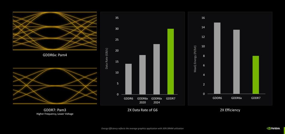
In 2024, Micron announced GDDR7, the next leap in graphics double data rate memory. With 32 Gb/s per pin, it delivers over 1.5 TB/s system bandwidth on a 384-bit bus, surpassing GDDR6X by nearly 50%. [5]
The standard introduces four independent channels per device, improving parallelism and bus utilization, particularly in multi-threaded GPU workloads. This finer granularity reduces latency under random access conditions, though it increases controller command complexity and pin count.
GDDR7 also claims a >50% improvement in power efficiency relative to GDDR6, achieved through lower voltage operation, enhanced signaling, and optimized refresh cycles.
Instead of PAM4, GDDR7 adopts PAM3 signaling, which uses three voltage levels (0, 1, 2) to encode 1.5 bits per UI. This strikes a balance between PAM2’s simplicity and PAM4’s high density. The four channels in GDDR7 will provide finer granularity and improved utilization, albeit at the cost of more command pins. Engineers should prepare for new controller designs and training methodologies.
Competing Technologies
While GDDR7 extends the life of discrete GPU memory, other technologies address different system classes:
HBM2E and HBM3 leverage 3D-stacked DRAM with 1024–2048-bit interfaces, achieving >2 TB/s bandwidth. Despite superior throughput, their cost, TSV packaging, and thermal constraints limit adoption to AI accelerators and supercomputers.
LPDDR5X targets mobile and low-power edge devices, offering up to 8533 MT/s using NRZ signaling and narrow buses. It prioritizes power efficiency and compact form factors over extreme bandwidth.
CXL and PCIe-based memory expansion technologies introduce disaggregated memory pools, enabling shared access across heterogeneous compute nodes. While not direct competitors to GDDR, they illustrate a broader memory hierarchy diversification trend in AI and cloud architectures.
The transition from GDDR6 to GDDR7 represents a paradigm shift in graphics memory design, combining higher data rates, improved efficiency, and smarter signaling schemes.
Recommended Reading: High Bandwidth Memory: Concepts, Architecture, and Applications
Conclusion
For digital design engineers and hardware architects, selecting between GDDR6 and GDDR6X involves balancing bandwidth, power efficiency, cost, and design complexity. GDDR6 provides a stable, standardized ecosystem with dual-channel architecture, error detection, and moderate power draw, making it ideal for professional GPUs, AI inference, and embedded systems. GDDR6X, through PAM4 signaling, delivers up to 50% higher bandwidth and improved energy per bit, powering ultra-high-performance GPUs like RTX 4090 by Nvidia. Looking ahead, GDDR7—using PAM3 signaling and multi-channel interfaces—will bridge the gap toward HBM-class throughput, redefining memory bandwidth for future AI, HPC, and graphics workloads.
Frequently Asked Questions
1. Is GDDR6X always better than GDDR6?
A. Not necessarily. GDDR6X provides higher bandwidth and better energy per bit, but it also demands more complex controller designs, increased power delivery, and tighter signal integrity. For many professional and embedded applications, GDDR6 offers sufficient throughput with lower risk and cost.
2. Can GDDR6X be used with ECC?
A. ECC is not built into GDDR6X; error detection features such as CRC are available. ECC can be implemented in the memory controller, but few controllers currently support it. Therefore, mission‑critical systems often prefer GDDR6 with full ECC support.
3. Why does GDDR6X have the same burst length per access despite a lower BL value?
A. PAM4 signaling in GDDR6X transmits two bits per symbol. Although its burst length is BL8 versus BL16 in GDDR6, each unit interval carries two bits, so each channel still delivers 32 bytes per burst.
4. How does PAM4 improve energy efficiency?
A. By encoding two bits per symbol, PAM4 halves the symbol frequency for a given data rate. This lowers the I/O’s switching frequency and reduces dynamic power. Micron reports ~7.25 pJ/bit for GDDR6X vs 7.5 pJ/bit for GDDR6.
5. What factors determine whether a GPU uses GDDR6 or GDDR6X?
A. GPU manufacturers consider target performance, cost, power budget, and market segment. Flagship gamers and top-tier benchmarks favor GDDR6X, while workstations and AI CPUs use GDDR6 for ECC, capacity, and broader vendor support from Samsung and Micron.
6. Will GDDR6X replace GDDR6?
A. Not soon. GDDR6X dominates high-fps gaming GPUs, but GDDR6 remains ideal for DDR5-class midrange graphics, AI modules, and embedded boards needing efficient memory speed without premium signal specs or cost overhead.
7. How do I prepare for GDDR7?
A. GDDR7 will use PAM3 signaling with multi-channel memory modules, blending PAM2 simplicity and PAM4 density. Engineers should study the design of GDDR6X, upgrade simulation tools, and review benchmarks for emerging Samsung and Micron specs.
References
[1] Micron. Micron Innovates From the Data Center to the Edge With NVIDIA [Cited 2025 September 28] Available at: Link
[2] ResearchGate. 16-Gb, 18-Gb/s/pin GDDR6 DRAM With Per-Bit Trainable Single-Ended DFE and PLL-Less Clocking [Cited 2025 September 28] Available at: Link
[3] MDPI. Greedy Prefetch for Reducing Off-Chip Memory Accesses in Convolutional Neural Network Inference [Cited 2025 September 28] Available at: Link
[4] Huawei. What Is PAM4? What Are the Advantages of PAM4? [Cited 2025 September 28] Available at: Link
[5] Micron. Micron Samples Next-Gen Graphics Memory for Gaming and AI [Cited 2025 September 28] Available at: Link
in this article
1. Introduction2. Evolution of GDDR and the Rise of GDDR6X3. Memory Architecture and Prefetching4. Signaling and Encoding: NRZ vs PAM45. Bandwidth, Data Rates, and Capacity6. Power Consumption and Thermal Implications7. Board Design, Controller Complexity, and Training8. Design Considerations for Engineers9. Use Cases and Emerging Applications10. Future Trends: GDDR6X Improvements and GDDR711. Conclusion12. Frequently Asked Questions13. References