Electronics That Bend the Rules: The Benefit of Flexible Multilayer Designs
Flexible Multilayer Electronics combine flexibility with advanced functionality, enabling applications in wearables, biosensors, defense, and consumer electronics. This article explores how technologies like Voltera’s NOVA platform are making their development more accessible.

05 Feb, 2025. 7 minutes read

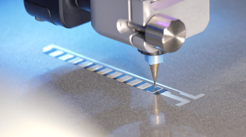
NOVA dispensing ink for a flexible membrane keyboard
In the world of electronic manufacturing, printed circuit boards (PCBs) still reign. However, their applications have remained limited due to their rigid nature. Flexible electronics have therefore been on the rise as an alternative to PCBs, offering electronic circuits that can bend, stretch, and even wrap around other objects. This adaptability enables them to be integrated into a wider variety of surfaces and products. However, single layer flexible electronics lack the advanced performance capabilities of rigid PCBs, which also creates limitations in terms of their use. That’s where Flexible Multilayer Electronics come in. This emerging type of circuitry, made possible through technologies like Voltera’s NOVA platform, delivers the benefits of flexible electronics while enabling more complex functions.
What Are Flexible Multilayer Electronics?
Flexible Multilayer Electronics bear some similarities to Flexible Hybrid Electronics (FHE), which bridge the divide between PCBs (powerful but rigid) and flexible printed electronics (bendable but largely limited to simple applications like sensors and displays).[1] However, unlike FHEs, Flexible Multilayer Electronics do not include rigid PCBs or integrated circuits (ICs). Instead, they build on functionality by layering circuitry printed onto flexible substrates. The result is electronics that are more complex in their functionality and highly conformable.
One of the defining characteristics of flexible electronics is the use of flexible substrates, such as PET or TPU. Stretchable conductive inks, such as Stretchable Silver Ink are then applied to the substrate using a precision printing process, such as inkjet printing or direct ink writing. With Flexible Multilayer Electronics, this initial base layer is followed by the application of a dielectric layer, where an insulating ink is selectively printed onto the base layer. From there, the third layer, or crossover layer, can be applied, which adds further conductive properties to the circuit.
The functionality of Flexible Multilayer Electronics has obvious benefits, such as being able to create stretchable, lightweight, and compact electronics that can conform to a wide variety of surfaces, like textiles, IoT devices, and even skin.
The Technology Enabling Flexible Multilayer Electronics Development
The ability to manufacture Flexible Multilayer Electronics has recently been unlocked on Voltera’s NOVA materials dispensing system thanks to a recent Plan software upgrade. NOVA, a printing platform for flexible hybrid electronics R&D and novel materials research, enables the printing of viscous materials onto various substrates. This includes flexible PET, stretchable TPU, conformable paper, and biocompatible polyimide, as well as rigid substrates like FR1, FR4, silicon wafers, and more. NOVA is particularly notable for its ability to print a wide range of materials with viscosities ranging from 1,000 to 1,000,000 cps. In practice, this means NOVA can process a variety of conductive, dielectric, or functional inks, as well as gels and pastes.[2]
NOVA is a useful tool for prototyping flexible multilayer electronics as well as making custom electronics, materials testing, and manufacturing low-volume batches. These capabilities are further enhanced thanks to the company’s latest software feature, Plan. This software upgrade is integral to the production of Flexible Multilayer Circuits as it enables users to print up to four stackup layers for enhanced functionality and gives users greater control over the sequence of trace printing.
More specifically, Plan allows users to visualize and edit the print sequence of multilayer electronic designs, while identifying potential errors before the printing begins. The tool also automatically generates smart probe points, which results in more accurate heightmaps based on the layer stackup. These features ultimately unlock the creation of repeatable, consistent multilayer prints and facilitate the production of multi-signal paths, complex sensor networks, and more complex routing in flexible electronics.
Voltera developed NOVA with the aim of transforming how printed electronics—in particular, flexible electronics—are developed and manufactured. The modular printing platform empowers users to develop, iterate and test flexible electronics, as well as custom materials, in a time- and cost-efficient manner. For example, users can iterate their flexible electronic designs in-house within just a day, rather than having to wait days or weeks through a vendor. For multilayer designs, being able to iterate in-house and identify errors before printing is notably beneficial, since more traditional production methods for multilayer electronics, like screenprinting, which typically necessitate working with external vendors, can be incredibly time consuming and require significant back and forth before a correct screen design is reached.
On top of that, NOVA allows for more economical material use, since the conductive and dielectric inks are applied selectively and with precision, unlike screen printing methods that consume more material, requiring a screen for every layer. These material and cost advantages are especially notable in multilayer prints, where screenprinting additional layers can drive up costs significantly. By contrast, with NOVA, the only added costs are for the ink used in the extra layers.
Applications of Flexible Multilayer Electronics
Understandably, the ability to rapidly iterate and make Flexible Multilayer Electronics will have big impacts in industries like healthcare, defense, and consumer electronics, all of which can benefit from lightweight, conformable, and highly functional electronics. Below are just a few examples of how end users are exploring the use of flexible electronics and how multilayer printing could transform these applications.
Biosensing
In the healthcare sector, flexible multilayer electronics are opening up unprecedented opportunities when it comes to health monitoring and biosensing. More specifically, integrated circuitry and sensors on flexible and biocompatible substrates can be used for a range of medical uses, including diagnostics, drug delivery, and general wellness tracking. Flexible multilayer electronics can be placed directly on the body or integrated into a wearable device to gather valuable data on things like glucose levels, intracranial pressure, wound monitoring, and more.[3] For example, Voltera recently demonstrated the ability to print multi-material ECG sensors using biocompatible gold and stretchable silver ink—a function facilitated by Plan software.

Field Operations
Flexible multilayer electronics can also be game-changing for field operations in the automotive and defense sectors. There are many possible uses for flexible multilayer electronics: for example, they can be used in harsh environments, offering ruggedized, conformable electronics that can be mounted on vehicles, drones, soldiers, and robots. The U.S. Department of Defense, for instance, has invested in flexible electronics with the aim of advancing applications like soldier network authentication, infrastructure monitoring [4], communications systems, and even drone operations.[5] In this vertical, multilayer printing capabilities could enable greater functionality for conformable sensors and faster development times for new devices.
Consumer Electronics
With the growing demand for miniaturization in the consumer electronics industry, flexible multilayer electronic technology is playing an increasingly important role. With the ability to integrate more complex circuitry and multiple materials on flexible, stretchable substrates, consumer electronics companies are ushering in new and innovative products like smartphones with foldable screens, electronic textiles, and compact, flexible batteries. For example, Huawei released a smartphone with a screen that folds three ways, which when unfolded is the slimmest phone ever.[6] Additionally, Voltera recently designed a multilayer flexible membrane keyboard. This design, which integrated three layers, resulted in a thin, lightweight keyboard that could have applications in portable electronics, toys, home appliances, and more.
The Future of Flexible Multilayer Electronics
The field of Flexible Multilayer Electronics is a burgeoning one and its potential only continues to grow as applications evolve and production platforms like Voltera’s NOVA make flexible electronics development more accessible to researchers and product developers through its short turnaround times and versatile material choice. Interestingly, the ongoing growth and advancement of flexible electronics is very much the result of multi-disciplinary collaboration. Engineers, researchers, and electronics companies and manufacturers are coming together to develop new solutions and usher in a new era for wearable devices and conformable electronics.
For example, researchers based out of Polytechnique Montreal are leveraging Voltera’s NOVA to develop bioelectronics that use self-healing materials as a substrate. Among the projects being pursued are flexible sensors that can be mounted on violin bows to improve performance and tennis rackets that help minimize the risk of injury.[7]
Voltera also demonstrated NOVA’s ability to produce Flexible Multilayer Electronics by printing an electroluminescent, blue-light-emitting pattern onto both a paper and PET substrate. This project, which leveraged electroluminescent ink, consisted of printing four layers: a base conductive layer, a dielectric layer, a phosphor layer (necessary for the electroluminescent effect), and a top conductive layer. The result was a glowing circuit in the pattern of Voltera’s logo—a capability that the company says could be extended to applications like billboards, control panels, and branded merchandise.

This is truly just the tip of the iceberg when it comes to the future of Flexible Multilayer Electronics. The emerging field is developing quickly and is ripe for innovation. Whether you’re looking to develop flexible multilayer circuits in-house, printing novel electronics, or testing materials for your research, contact Voltera to learn more.
References
[1] Franz, Jillian. What are Flexible Hybrid Electronics? [Internet]. Voltera, December 8, 2024.
[2] NOVA materials dispensing system [Internet]. Voltera, 2024.
[3] Next-generation health monitoring requires the integration of flexible hybrid electronics (FHE) [Internet]. Medical Design & Outsourcing, November 6, 2023. https://www.medicaldesignandoutsourcing.com/flexible-hybrid-electronics-fhe-next-generation-health-monitoring/
[4] DOD awards $154 million to Army-led flexible electronics project [Internet]. U.S. Army, July 15, 2020. https://www.army.mil/article/237275/dod_awards_154_million_to_army_led_flexible_electronics_project
[5] Flexible Hybrid Electronics Demonstrator for UAV Applications. Department of Defense Manufacturing Innovation Institutes. https://www.dodmantech.mil/Portals/107/Flexible%20Hybrid%20Electronics%20Demonstrator%20for%20UAV%20Applications%20%20NextFlex.pdf
[6] Dayaram, Sareena. Mate XT Ultimate Design: What It Was Like Using Huawei's Sexy Triple-Screen Phone [Internet]. CNET, Oct. 2, 2024. https://www.cnet.com/tech/mobile/what-it-was-like-using-mate-xt-ultimate-design-huaweis-tri-folding-phone/
[7] Polytechnique Montréal: Researching Printed Stretchable Bioelectronics with Voltera NOVA and V-One [Internet]. Voltera, 2024.