AND Truth Table: Boolean Logic, Gate Symbols & Applications
Learn how the AND truth table works, understand how AND gates are shown in circuit diagrams, and where they are used in real systems.

22 May, 2026. 12 minutes read

Key Takeaways
The AND operation gives a true output only when all inputs are true. Its Boolean expression is written as Q = A·B or A∧B.
A two-input AND gate has four possible input combinations. The output is high (1) only when both inputs are high.
A three-input AND gate has eight rows in its truth table. The output is 1 only when all three inputs are 1. Likewise, for n inputs, there are 2ⁿ combinations.
There are two standardized symbol sets: the distinctive-shape symbols (flat-front for AND) and the IEC rectangular symbols. ANSI/IEEE uses distinctive shapes, while IEC 60617 prefers rectangles.
Real-world AND gates are built in TTL (for example, 74LS08) with propagation delays of around 19-27 ns and in CMOS (for example, 74HC08) with delays of around 7-12 ns.
NAND, OR, NOR, XOR, and XNOR gates offer complementary operations. NAND is the logical negation of AND, while XNOR (biconditional) outputs true when inputs are equal.
Introduction
From simple microcontrollers to powerful computers, digital systems work with binary signals that have only two possible values: 0 (false) and 1 (true). Boolean logic explains how those signals combine, and the AND operation is one of the most basic and important parts of that system. It means that the input conditions must all be true for the final result to be true.
Engineers use truth tables to show exactly how a logic operation behaves. A truth table lists every possible input combination and the output that goes with it. Because of that, truth tables are a clear and reliable way to describe logic functions in electronics and computer design.
This guide explains the AND operation from both the mathematical and hardware aspects. It covers standard notation, truth tables for two- and three-input cases, important Boolean algebra rules, comparisons with other logic gates, and the implementation of AND gates in actual circuits. It also looks at practical uses such as enabling signals, bit masking, and address decoding.
What Is the AND Operation
At its simplest, the AND operation is a logical conjunction. The output is true only if all inputs are true. In Boolean algebra, the operation between A and B can be written in a few common ways:
A · B (multiplication symbol, often written AB)
A ∧ B (logical AND)
A and B (sometimes the word "and" is written explicitly)
The symbol may look like multiplication, but AND works on truth values, not ordinary numbers. It is similar to multiplication in one simple way: 1 AND 1 gives 1, while any input of 0 makes the result 0. So, it’s a little hack to understand the AND operation. But beyond that, Boolean logic follows its own rules.
A simple way to remember AND operation is that ”If an AND gate has more than one input, the output becomes true only when every input is true.” That is the key idea behind the entire operation.
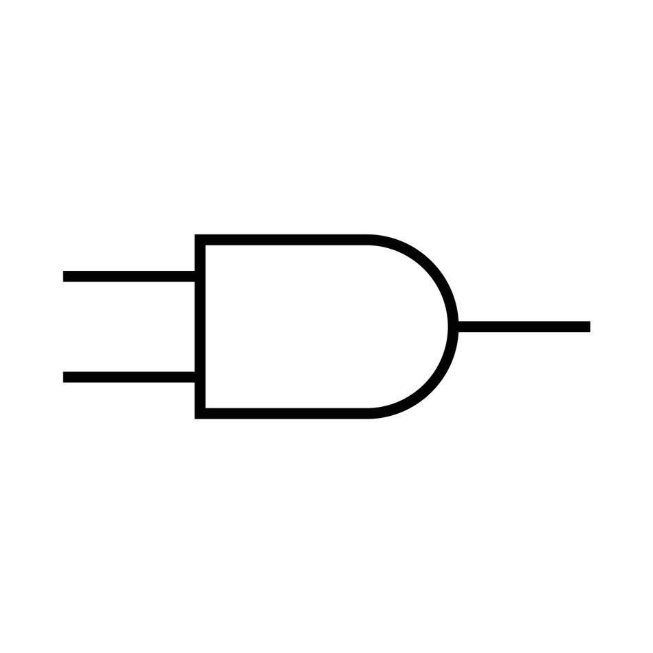
In hardware, the AND operation is performed by a logic gate. It’s an electronic circuit designed to perform a Boolean function. AND gates are shown using standard symbols.
One common style uses the familiar flat-front gate shape, while the IEC style uses a rectangle with input and output lines. Engineers choose the symbol style based on the design standard they follow and on what makes the schematic easiest to read.
The 2-Input AND Truth Table
Truth Table and Logic Values
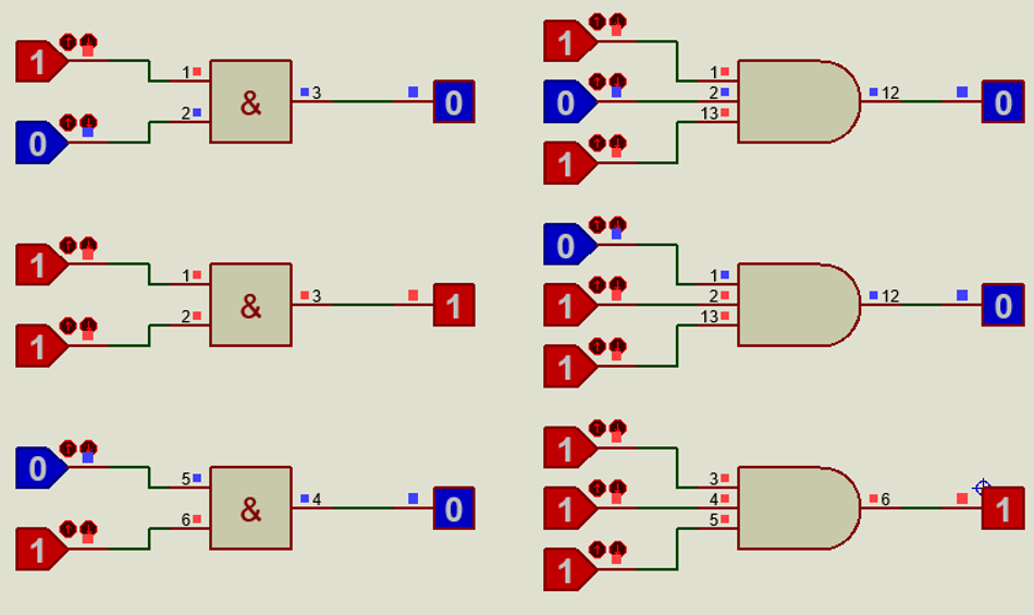
A two-input AND gate has four possible input combinations: 00, 01, 10, and 11. The truth table shows the output for each case. According to the DM7408 TTL datasheet, the output is high only when both inputs are high. In every other case, the output is low.
A | B | Output Q = A·B |
0 | 0 | 0 |
0 | 1 | 0 |
1 | 0 | 0 |
1 | 1 | 1 |
The last row (A = 1, B = 1) is the only row where all inputs are 1, producing 1 at the output. The logical expression for the AND gate is
Q = A · B
Multi-Input AND Truth Tables
Three-Input AND Gate
A three-input AND gate extends the operation by requiring all three inputs to be true for the output to be true. The truth table has eight rows because there are 2³ = 8 combinations. Experiments confirm that the three-input AND gate outputs 1 only when all three inputs are 1. The Boolean expression for a three-input AND gate is given as:
Q = A . B . C
The following table lists all combinations.
A | B | C | Output |
0 | 0 | 0 | 0 |
0 | 0 | 1 | 0 |
0 | 1 | 0 | 0 |
0 | 1 | 1 | 0 |
1 | 0 | 0 | 0 |
1 | 0 | 1 | 0 |
1 | 1 | 0 | 0 |
1 | 1 | 1 | 1 |
Only the last row (111) yields an output of 1.
Generalization for n-Input AND Gates
For an AND gate with n inputs, the truth table has 2ⁿ rows, representing every combination of input truth values. The output is 1 only when all inputs are 1. Otherwise, it is 0. This exponential growth matters in design verification, as testing every input combination quickly becomes impractical for large n.
Techniques such as symbolic simulation and formal verification help manage complexity, but the fundamental rule remains: the AND operation serves as a universal "all conditions must hold" test.
Recommended Reading: NAND Truth Table: A Comprehensive Guide for Digital Designers and Hardware Engineers
AND in Boolean Algebra
Boolean algebra uses algebraic manipulation to simplify logic expressions and design efficient circuits. The AND operation obeys several fundamental identities and laws that allow simplification and understanding. The following table summarizes the laws and their mathematical expressions:
Law | Mathematical Expression | Description |
Identity Law | A . 1 = A | Multiplying (AND) a value by 1 or adding (OR) a value by 0 doesn’t affect the operand. |
Annihilator Law | A . 0 = 0 | AND an input with 0 returns a 0. OR an input with 1 will return a 1. In both cases, the value of the input operand is ignored. |
Idempotent Law | A . A = A | When AND or OR is performed with identical inputs, the output follows the input operand. |
Complement Law | A . A’ = 0 | When a variable AND its own complement, the output is 0, when it is OR-ed with its complement, the output is 1. |
Commutative Law | A . B = B . A | The order of inputs doesn’t affect the output |
Associative Law | (A.B).C = A.(B.C) | The grouping of inputs doesn’t affect the output |
Distributive Law | A . (B + C) = (A + B).(A + C) A + ( B . C) = (A + B) .(A+C) | AND and OR operations distribute over each other. This is a critical law for simplifying Boolean Expressions. |
Absorption Law | A + A.B = A | Repeated terms can be removed |
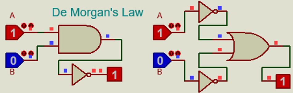
De Morgan’s Law | (A . B)’ = A’ + B’ | The complement of AND conjunction equals the OR disjunction of the complements, and the complement of an OR disjunction equals the AND conjunction of the complements |
The figure below shows the mathematical expressions for the laws discussed above.
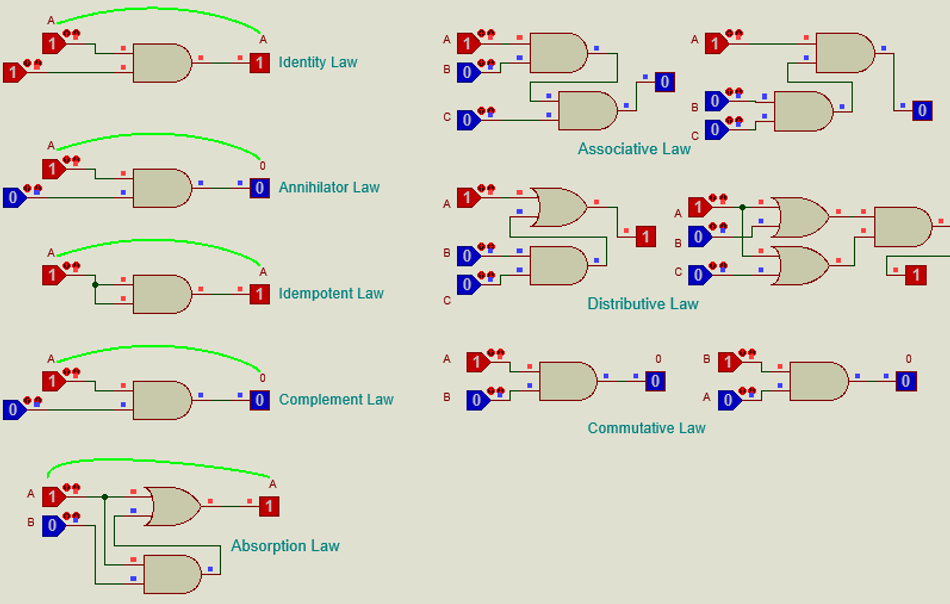
Boolean identities simplify complex expressions. For example, A·B + A·B' = A (applying distributive and complement laws). Mastering these laws leads to more efficient digital designs with fewer gates and lower propagation delay.
Significance of De Morgan’s Law in Boolean Algebra
De Morgan’s Law is one of the fundamental laws in Boolean Algebra. It lets you express the AND functions as OR functions with negations, and vice versa. The law also underlies the equivalence of certain logic symbols.
AND Gate in Hardware
Integrated Circuits and Propagation Delay
The AND operation is realized in physical hardware using integrated circuits (ICs). Transistor-Transistor Logic (TTL) and Complementary Metal-Oxide-Semiconductor (CMOS) are two common logic families.
Suggested Reading: Transistor Circuit Design – Theory and Practice for Modern Engineers
TTL (74LS08 Quad 2-Input AND Gate): The DM7408 datasheet shows a function table confirming that the output is high only when both inputs are high.
Switching characteristics indicate typical propagation delays of about 27 ns for low-to-high and 19 ns for high-to-low transitions. TTL gates drive moderate fan-out and draw more current than CMOS.
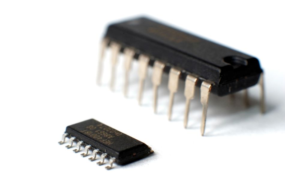
CMOS (74HC08 Quad 2-Input AND Gate): The 74HC08 features much lower power consumption and faster response. Typical propagation delays are around 12 ns (low-to-high) and 7 ns (high-to-low) at 5V. CMOS gates have high input impedance and can drive multiple TTL loads, with a fan-out of about 10 LS-TTL loads .
Differences in propagation delay and power consumption influence design decisions. High-speed applications may favor TTL or advanced families such as ECL (emitter-coupled logic), while battery-powered or high-density circuits tend to favor CMOS.
Transistor-Level Implementation
Understanding the transistor-level implementation reveals why the AND gate behaves as it does.
NMOS and PMOS networks: In CMOS logic, the AND function is realized by placing NMOS transistors in series in the pull-down network and PMOS transistors in parallel in the pull-up network. A pair of NMOS transistors connected between output and ground conduct only when both gate inputs are high, pulling the output low.
Complementary PMOS transistors connect the output to the supply in parallel, conducting when either input is low and pulling the output high. This complementary arrangement ensures that only one path (pull-up or pull-down) is conducted at a time, reducing static power consumption.
Suggested Reading: PMOS vs NMOS: Unraveling the Differences in Transistor Technology
Propagation delay and fan-out: Propagation delay arises from transistor capacitances and the time required to charge or discharge the load. The series NMOS arrangement adds resistance, increasing delay with more inputs.
Designers reduce delay by limiting the number of transistors in series or using faster logic families. Fan-out describes how many gate inputs a single output can drive. CMOS typically supports high fan-out due to its low input current, but the load capacitance affects speed.
Standard Logic Symbols
AND gates are shown with standard symbols in circuit diagrams. The distinctive-shape version uses a flat front and curved back. The IEC version uses a rectangle with labeled function behavior. Small circles, often called bubbles, can be added to show negation or active-low signals. For example, putting a bubble on the output of an AND gate turns it into a NAND gate
Hardware and circuit diagrams show AND gates with standard symbols. The distinctive-shape symbol uses a flat front (flat-sided semicircle) to represent the AND function. It is also the ANSI representation of the AND gate.
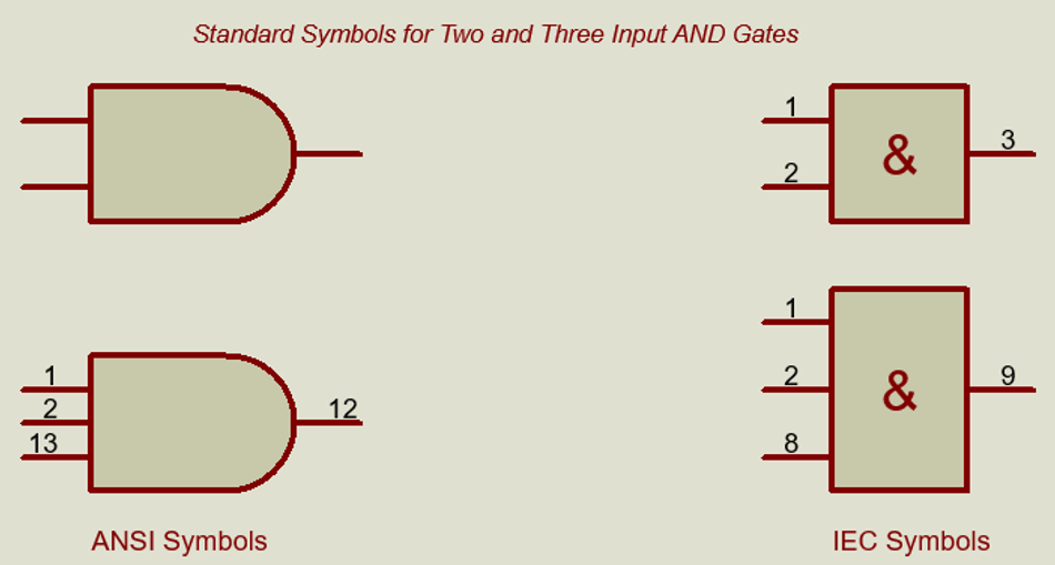
The alternative rectangular symbol is given by IEC 60617. It shows all gates as rectangles with function labels. Both symbols may include "bubbles" (small circles) on inputs or outputs to denote negation or active-low signals. For example, adding a bubble to the output of an AND symbol converts it into a NAND gate.
Recommended Reading: Understanding Logic Gate Symbols: Comprehensive Guide for Engineers
AND Gate vs Other Logic Gates
Understanding how the AND operation contrasts with other fundamental logic gates highlights its role in Boolean logic and digital design. Table 3 compares the outputs of common two-input gates for all input combinations.
A | B | AND (A·B) | NAND ((A·B)') | OR (A+B) | NOR ((A+B)') | XOR (A⊕B) | XNOR ((A⊕B)') |
0 | 0 | 0 | 1 | 0 | 1 | 0 | 1 |
0 | 1 | 0 | 1 | 1 | 0 | 1 | 0 |
1 | 0 | 0 | 1 | 1 | 0 | 1 | 0 |
1 | 1 | 1 | 0 | 1 | 0 | 0 | 1 |
NAND (Not AND) outputs the negation of AND: the output is false only when all inputs are true . NAND is a universal gate. Using only NAND gates, any Boolean function can be implemented. OR (disjunction) outputs true if at least one input is true.
NOR (Not OR) outputs true only when all inputs are false. XOR (exclusive OR) outputs true when inputs differ (exactly one true), acting like a parity checker. XNOR (exclusive NOR or biconditional) outputs true when inputs are equal (both true or both false).
NAND and NOR are universal because any logic operation can be composed entirely from NAND or NOR gates. De Morgan's laws reveal that negating an AND produces an OR of negations, which is why NAND and NOR complement the AND and OR functions. Designers often select NAND gates for integrated circuits due to manufacturing efficiency.
Applications of the AND Operation
The AND operation has countless applications across digital design, computer science, and software engineering.
Enable and Control signals
AND gates act as signal enablers. When a control input is 1, the signal passes through unchanged. When the control is 0, the signal is suppressed. Using an AND gate to mask a data line with an enable signal ensures that data reaches downstream logic only when permitted.
Bitwise Masking in Software
Many programming languages support the bitwise AND operator. To clear specific bits in an integer, a mask with 0s in the positions to be cleared is ANDed with the data.
The result zeros out those bits while leaving others unchanged. This technique is fundamental in systems programming, device drivers, and microprocessor register manipulation.
Address Decoding
AND gates detect specific binary patterns in address decoders. Cascading multiple AND gates allows detection of a word or peripheral when all relevant address lines match a programmed pattern.
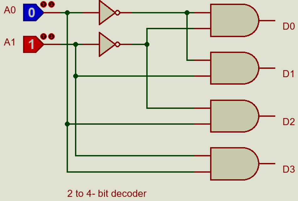
For example, an address decoder may drive a chip-select signal high only when the input lines match a pattern such as 0101, demonstrating that the AND gate's output becomes 1 only when all inputs match the code .
Conditional Logic in Control Flow
In processor architectures, conditional logic uses AND operations to decide whether to perform a task. For example, an interrupt logic circuit may AND an interrupt request with a global enable signal. In arithmetic circuits, partial products in binary multiplication are formed by ANDing bits.
Debouncing and Signal Synchronization
Glitches or noise on mechanical switches can be filtered by combining an input with synchronized timing signals through AND gates. When the switch is pressed, and the timing pulse is high, the output is high. Noise pulses outside the timing window are suppressed.
Networking and Communication Protocols
Checksums and parity bits often involve ANDing or XORing data bits. In digital logic operations for error detection, such as cyclic redundancy checks, partial products use AND operations to generate polynomial multiples.
Suggested Reading: UART Protocol: Understanding Serial Communication for Engineers
Conclusion
The AND operation is fundamental to Boolean logic, digital circuit design, and computer science. Its truth table shows that the output is true only when all inputs are true . This simple rule underpins complex systems: enabling or disabling signals, enforcing conditions in software, decoding addresses, and constructing universal logic functions. Boolean algebra provides identities and laws that simplify AND expressions and reveal relationships to other operations, including De Morgan's laws .
In hardware, AND gates come in integrated circuit packages like the TTL 74LS08 and CMOS 74HC08. TTL gates exhibit propagation delays around 19-27 ns , while CMOS gates offer lower power and delays around 7-12 ns . At the transistor level, series NMOS transistors implement the AND function, and complementary PMOS networks provide the pull-up path . Understanding these implementations helps engineers optimize speed, power, and fan-out.
FAQs
What is the AND truth table?
The AND truth table lists all possible input combinations and their outputs for the AND operation. For two inputs A and B, there are four rows: when either input is 0, the output is 0. Only when both inputs are 1 does the output become 1 . The truth table is crucial because it provides a complete specification of the logical AND function.
How many rows are in a 3-input AND truth table?
A three-input AND gate has eight possible input combinations (2³ = 8) . The output is 1 only when all three inputs are 1 . The remaining seven combinations produce 0.
What is the Boolean expression for AND?
The AND operation between two variables A and B is written as A·B, AB, or A∧B. The dot represents logical multiplication and should not be confused with arithmetic multiplication, even though the truth table resembles multiplication of binary values .
What's the difference between AND and NAND?
The NAND gate outputs the negation of the AND function. For the same inputs, NAND produces 0 only when all inputs are 1. Otherwise, it outputs 1 . Because NAND combines AND and negation, it serves as a universal gate. Any Boolean function can be implemented solely with NAND gates.
Is multiplication the same as the AND operation?
The AND operation resembles binary multiplication: 1 AND 1 yields 1, and any AND with 0 yields 0. However, Boolean algebra and arithmetic operate in different domains. Boolean variables take only two values (0 and 1), and operations follow Boolean algebra laws such as De Morgan's theorems. Arithmetic multiplication has properties like associativity over real numbers, whereas logical AND applies only to truth values.
Which IC contains AND gates?
Common ICs containing AND gates include the TTL 74LS08 and CMOS 74HC08, each providing four two-input AND gates. The 74LS08 has typical propagation delays of 19-27 ns , while the 74HC08 offers lower power and delays of 7-12 ns . Many microcontrollers and programmable logic devices also embed AND gates in larger functional blocks.
What is the XNOR (biconditional) gate, and how does it relate to AND?
The XNOR (exclusive NOR) gate outputs 1 when its inputs are equal (both 0 or both 1) . It represents logical equivalence, also called biconditional. Although not directly related to AND, XNOR uses the AND operation in its internal implementation. For example, XNOR equals (A·B) + (A'·B'). It is useful in comparators and equality checks.
How does the number of inputs affect propagation delay?
Increasing the number of inputs in an AND gate typically increases propagation delay because additional transistors are connected in series in the pull-down network. More transistors in series means greater resistance and capacitance, and longer charge or discharge times . Designers often limit input count or use tree structures to reduce delay.
References
Electronics Tutorials, “Logic AND function – digital logic gates,” Electronics-Tutorials.ws, [Online]. Available: http://www.electronics-tutorials.ws/boolean/bool_1
“Logic gates with truth table [AND, OR, NAND, NOR],” The Engineer’s Post, [Online]. Available: https://www.theengineerspost.com/logic-gates-with-truth-table/
“Logic gate symbols (digital electronic),” Electrical‑Symbols.com, [Online]. Available:https://www.electrical-symbols.com/electric-electronic-symbols/logic-gates-symbols.htm
“Characteristics of logic gates,” KFUPM COE‑202 course notes, [Online]. Available: https://faculty.kfupm.edu.sa/coe/mudawar/coe202/lectures/05-CharacteristicsOfLogicGates.pdf
“AND gate,” GeeksforGeeks‑Digital Logic, [Online]. Available: https://www.geeksforgeeks.org/digital-logic/and-gate/
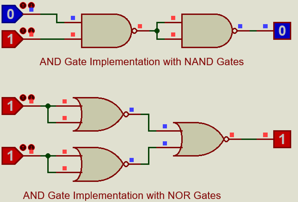
“Implementation of AND gate from NOR gate,” GeeksforGeeks‑Electronics Engineering, [Online]. Available: https://www.geeksforgeeks.org/electronics-engineering/implementation-of-and-gate-from-nor-gate/
“Implementation of AND gate from NAND gate,” GeeksforGeeks‑Digital Logic, [Online]. Available: https://www.geeksforgeeks.org/digital-logic/implementation-and-from-nand/
“Multiple‑input gates,” in Digital Textbook, All About Circuits, [Online]. Available: https://www.allaboutcircuits.com/textbook/digital/chpt-3/multiple-input-gates/
Texas Instruments, “SN74LVC2G08 dual 2‑input positive‑AND gate datasheet (Rev. N),” Texas Instruments, [Online]. Available: https://www.ti.com/lit/ds/symlink/sn74lvc2g08.pdf
“Logic gates – truth table and theory,” Virtual Labs, IIT‑Roorkee, [Online]. Available: https://de-iitr.vlabs.ac.in/exp/truth-table-gates/theory.html