Unlocking Large-Area Electronics with Direct Ink Writing
Explore how Direct Ink Writing (DIW) and Voltera's NOVA system are revolutionizing electronics prototyping—enabling flexible, stretchable, and large-area electronics for next-gen applications in healthcare, consumer tech, and automotive industries.

06 Aug, 2025. 5 minutes read
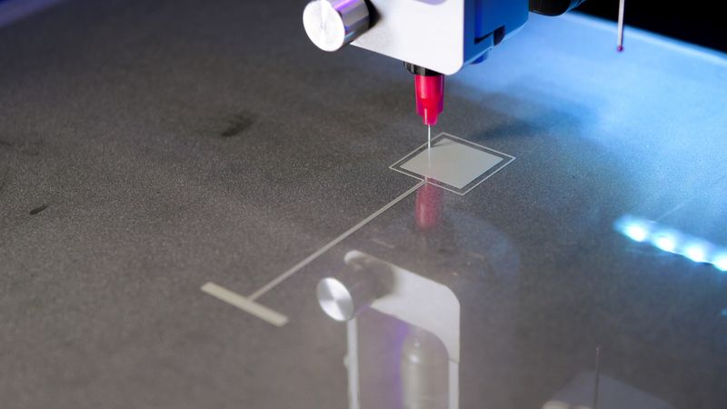
Voltera’s NOVA dispensing conductive silver ink for a flexible capacitive touch sensor.
Electronic devices have evolved tremendously in recent years, moving beyond standard-sized rigid, silicone chips to include increasingly versatile sensors and circuits, including flexible electronics, miniaturized electronics, and large-area electronics (LAE).
These new frontiers in the electronics industry are in large part enabled by emerging prototyping technologies, like Direct Ink Writing (DIW), which make it possible to print electronics directly—without the need for tools—and to use a broad array of materials, including flexible substrates and stretchable conductive inks. As we’ll see in this article, DIW solutions, such as Voltera’s NOVA materials dispensing system, are facilitating the development of novel large-area electronics applications, which could change the game for electronic devices in the healthcare, consumer, and automotive segments, among others.
What are Large-Area Electronics?
If you haven’t heard the term before, LAE is a cutting-edge field in the broader electronics industry that is focused on the development of ultra-thin, flexible electronics that can cover a wide area and, in many cases, conform to non-planar surfaces. LAE is thus closely tied to flexible electronics, with the added element of scale.
Among the most common application areas for LAE are displays (i.e. liquid crystal displays) and photovoltaics (i.e. solar cells). As technologies that enable LAE continue to advance, however, more and more applications are being explored in a variety of sectors, including healthcare, consumer goods, automotive, packaging, and more. For example, the study “Materials and Applications for Large Area Electronics: Solution-Based Approaches”, published in the journal Chemical Reviews, highlights a number of LAE applications, including medical imaging arrays, flexible active matrix displays, printed radio frequency identification (RFID), and light-emissive flexible displays.[1]
These LAE applications and others like wearable sensors and smart textiles are largely made possible thanks to material advances and innovative printing technologies, which have unbound electronics from their original rigid state and are making it possible to create large-scale conductive patterns on thin, flexible substrates. Production technologies like inkjet printing, screen printing, and roll-to-roll printing use varying approaches to apply conductive traces onto a large-scale flexible substrate.
Challenges for LAE
The biggest challenges still facing LAE—despite the technical ability to print conductive patterns onto large swaths of substrate—are related to functionality and cost. LAE developers and research groups are working to establish a balance between the production of large-area electronics with a high level of functionality (at a microelectronic level) over a large area without dramatically driving up the cost of creating the required conductive patterns. That’s where Direct Ink Writing (DIW) is making an impact.
DIW’s central role in LAE prototyping
Direct Ink Writing is becoming a key technology in the development and advancement of LAE devices. DIW is a printing method that selectively dispenses a viscous material or ink onto a substrate. The dispensed material is then solidified using UV curing, air drying, or a chemical reaction, resulting in a stable printed pattern.
DIW is an incredibly versatile technology thanks to the broad range of materials it can process. For example, dispensing feedstocks can include conductive or dielectric inks—even those with flexible properties—while compatible substrates include anything from TPU and thin-film PET to paper and fabric. This material versatility is central to why LAE developers are increasingly turning to DIW in order to prototype new devices. The ability to test new conductive materials on unconventional substrates, including thin and flexible substrates, is a must in LAE development.
Not only does DIW enable LAE developers to rapidly test the compatibility of print materials and substrates, it also facilitates rapid design iteration and validation. With DIW solutions in house, R&D groups can print and immediately test components (including sensors, interconnects, etc.), performing mechanical stress tests to understand how the device’s functionality is influenced by stretching or bending as well as implementing other quality checks. This capability enables LAE developers to not only dramatically accelerate prototyping cycles but to maintain greater control over the development process and design iterations.
While DIW itself is not a full-scale production solution, the prototyping technology does facilitate the transition from development to manufacturing. This is because the DIW process is compatible with most screen printing materials, enabling developers to test their LAE devices on a smaller scale using the same conductive inks and substrates before moving into mass production.
Finally, compared to more conventional electronic prototyping workflows—which in the case of screen printing requires the production of a mask—Direct Ink Writing does not require any tooling. By directly printing conductive patterns onto a substrate, DIW eliminates the need for tooling, which has multiple knock-on benefits, including less material usage, faster lead times, and lower prototyping costs.
In summary, DIW offers several benefits to LAE developers:
Versatile material compatibility
Rapid design iteration and validation
Seamless transition to scalable production
Reduced prototyping costs
LAE innovators leverage Voltera solutions
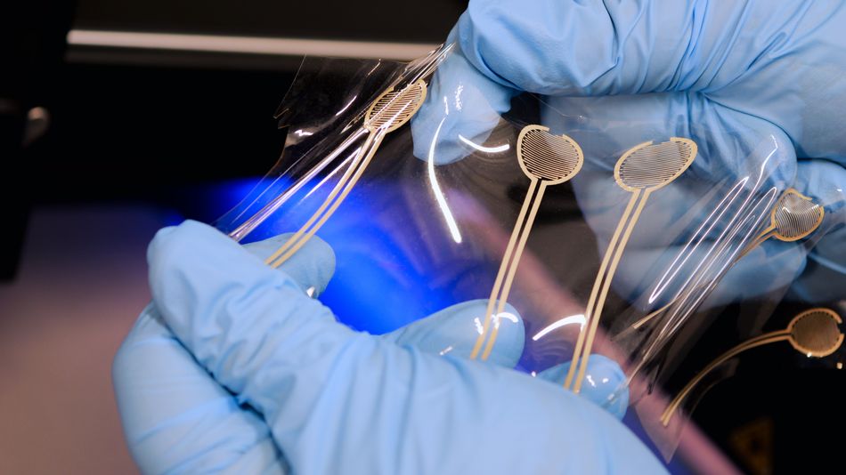
Canadian company Voltera is a leading provider of DIW solutions and the company’s technologies have supported many electronics R&D and product development efforts in recent years. Voltera’s flagship product is NOVA, a DIW-based materials dispensing platform capable of dispensing screen-printable materials into a wide range of substrates. The intuitive system has been used to develop myriad applications, from electrocardiogram (ECG) electrodes to printed batteries.
Because of its compatibility with a wide range of materials, NOVA is particularly well suited to LAE development and prototyping, enabling researchers to experiment with new material combinations and iterate designs quickly. In his 2023 thesis at the University of Surrey’s Advanced Technology Institute, for example, Georgios Bairaktaris leveraged one of Voltera’s printing platforms in the exploration of unconventional user interfaces. His work, which involved printing an augmented paper platform—the “Magic Bookmark”—using a combination of off-the-shelf parts and flexible printed conductors, demonstrated how simple fabrication processes and low-cost materials could be used to create large-area electronics.[2]
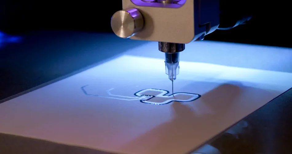
In another use case relevant to LAE, Voltera used its NOVA platform to print electroluminescent displays on paper and PET substrates. This application, which resulted in a blue-light emitting pattern in the shape of Voltera’s logo, is a good example of NOVA’s ability to print multilayer electronics. In this case, the electroluminescent display consisted of four layers: a base conductive layer, a dielectric layer, a phosphor layer, and a top conductive layer. According to the company this approach could also be applied to larger electronic displays, like billboards, control panels, and branded merchandise.
The future outlook of LAE
While large-area electronics is still very much an emerging field, and many potential use cases are still limited to the research realm, it has huge potential for healthcare, consumer, and industrial applications in terms of advancing the functionality of large-scale electronic displays and sensors, while also reducing costs.
With DIW platforms like Voltera’s NOVA empowering LAE developers, like those associated with the INNOLAE, to test out new materials and designs, we can expect to see many more LAE devices coming to market at competitive costs. Devices like large-scale venue displays; conformable solar skins, which could be designed to fit seamlessly onto buildings; wearable batteries or energy storage devices; smart bandages that monitor wound healing; textiles with thermal regulation built in; augmented e-paper; and much more. Overall, technologies like DIW are paving the way to LAE devices that are more functional, flexible, and lower cost.
References
[1] Arias AC, MacKenzie JD, McCulloch I, Rivnay J, Salleo A. Materials and applications for large area electronics: solution-based approaches. Chemical reviews. 2010 Jan 13;110(1):3-24.
[2] Bairaktaris G. Flexible electronic technologies for new user interfaces (Doctoral dissertation, University of Surrey).