Raspberry Pi Zero 2 W Pinout: Comprehensive Guide for Engineers
The Raspberry Pi Zero 2W features a quadcore 64 bit processor and builtin wireless in a tiny footprint. Its 40 pin header provides engineers with a flexible interface for embedded applications. This guide explores the theory behind the pinout and offers practical guidance for learners.

09 Dec, 2025. 12 minutes read
Key takeaways
The Raspberry Pi Zero 2 W uses a custom system‑in‑package (RP3A0) with a quad‑core Arm Cortex‑A53 CPU and 512 MB of LPDDR2 RAM. It delivers roughly five times the processing power of the original Pi Zero while retaining a 65 mm × 30 mm form factor
The 2×20 unpopulated header exposes 26 general‑purpose I/O lines plus power, ground and dedicated interfaces such as I²C, SPI, UART and PCM. It has a pinout identical to the 40‑pin layout used on the Pi 3/4 family.
Each GPIO can act as a digital input or output and supports alternate functions (e.g., PWM, clock, PCM). Engineers must respect the 3.3‑V maximum to avoid permanent damage.
The board provides 2.4‑GHz Wi‑Fi, Bluetooth 4.2/BLE, a mini‑HDMI port, CSI‑2 camera connector, micro‑USB OTG port and micro‑SD slot
Plan for safe power (5 V input), adequate thermal dissipation and correct pin numbering (physical vs BCM). Test pads on the underside provide reset, composite video and additional supply points
Introduction
Embedded design often requires balancing performance, size, and cost. The Raspberry Pi Zero 2 W addresses these challenges by combining a powerful quad‑core SoC, wireless connectivity and versatile GPIO in a module the size of a stick of gum. It was released as an upgrade to the original Pi Zero, so it shares the same footprint but increased CPU cores and memory through a custom RP3A0 system‑in‑package It includes 2.4‑GHz Wi‑Fi and Bluetooth 4.2/BLE along with a CSI‑2 camera interface and HAT‑compatible 40‑pin header Its affordable and offers a small form factor, making it attractive for IoT devices, digital design prototypes and embedded education.
This article dives deep into the Zero 2 W pinout. It explains how GPIOs are mapped, the electrical characteristics and the alternate functions supported by each pin. Practical examples illustrate how to drive LEDs, communicate with sensors via I²C/SPI/UART and generate PWM signals. We also cover design considerations such as power supply, signal integrity, and thermal management.
Suggested Reading: The Rise Of Raspberry Pi In Industrial Settings
Overview of the Raspberry Pi Zero 2 W
Hardware Specifications
The Raspberry Pi Zero 2 W is built around a Raspberry Pi‑designed system‑in‑package (RP3A0) that integrates a Broadcom BCM2710A1 SoC with 512 MB LPDDR2 RAM.
The quad‑core Arm Cortex‑A53 CPU runs at 1 GHz and offers about 40 % more single‑threaded performance and 5 times higher multi‑threaded performance than the single‑core Pi Zero. The following table summarises key specifications.
Parameter | Specification |
Processor | Broadcom BCM2710A1 quad‑core 64‑bit Arm Cortex‑A53 @ 1 GHz |
Memory | 512 MB LPDDR2 SDRAM |
Wireless | 2.4 GHz 802.11 b/g/n Wi‑Fi, Bluetooth 4.2 with BLE |
Video/Multimedia | Mini‑HDMI output, composite video via test pads, H.264/MPEG‑4 decode/encode (1080p30) and OpenGL ES 1.1/2.0 |
I/O connectors | 40‑pin GPIO header footprint, CSI‑2 camera connector, micro‑USB OTG, micro‑USB power, micro‑SD card slot |
Power | 5 V DC input (2.5 A recommended) |
Form factor | 65 mm × 30 mm board with unpopulated header |
Operating temperature | –20 °C to +70 °C |
Comparing Zero 2 W with the original Zero W
CPU and memory – The original Pi Zero W had a single‑core 1 GHz ARM11 and 512 MB RAM. The Zero 2 W retains the memory size but upgrades to a quad‑core ARM Cortex‑A53 with 64‑bit support.
Wireless – Both boards include 2.4‑GHz Wi‑Fi and Bluetooth but the Zero 2 W supports Bluetooth 4.2/BLE with improved RF compliance.
Power and form factor – The boards share the same 65 × 30 mm footprint and micro‑USB power. However, the Zero 2 W can draw more current during heavy processing, so a 5 V 2.5 A supply is recommended
Thermal design – To handle the additional cores, the Zero 2 W uses thick internal copper layers to conduct heat away from the processor. Designers may add a heatsink or ensure adequate ventilation.
Suggested Reading: The life of Pi: Ten years of Raspberry Pi
Understanding the 40‑pin GPIO Header
The 2×20 header on the Zero 2 W is unpopulated, allowing engineers to choose whether to solder male, female, or right‑angle headers. Pin 1 is denoted by a square pad on the underside, and physical numbering increases along the top row (odd numbers) and bottom row (even numbers).
The header provides 40 connections: two 5 V pins, two 3.3 V pins, eight ground pins and 26 GPIOs. The following table lists each pin’s physical position, Broadcom (BCM) GPIO number and primary function.
Physical pin | BCM GPIO / power | Primary function (default) | Description |
1 | 3V3 | 3.3 V power | Provide 3.3 V supply; up to ~500 mA available |
2 | 5 V | 5 V power | Direct supply from the micro‑USB input |
3 | GPIO 2 | I²C SDA1 | Data line for I²C bus (SDA1) |
4 | 5 V | 5 V power | An additional 5 V supply |
5 | GPIO 3 | I²C SCL1 | Clock line for I²C bus (SCL1) |
6 | GND | Ground | Common ground reference |
7 | GPIO 4 | GPCLK0 | General‑purpose clock (GPCLK0) or GPIO |
8 | GPIO 14 | UART TXD0 | Transmit line for primary UART |
9 | GND | Ground | Ground reference |
10 | GPIO 15 | UART RXD0 | Receive line for primary UART |
11 | GPIO 17 | GPIO | General‑purpose I/O |
12 | GPIO 18 | PCM CLK / PWM0 | Pulse‑code modulation clock or PWM output |
13 | GPIO 27 | GPIO | General‑purpose I/O |
14 | GND | Ground | Ground reference |
15 | GPIO 22 | GPIO | General‑purpose I/O |
16 | GPIO 23 | GPIO | General‑purpose I/O |
17 | 3V3 | 3.3 V power | Second 3.3 V supply |
18 | GPIO 24 | GPIO | General‑purpose I/O |
19 | GPIO 10 | SPI0 MOSI | Master‑out, slave‑in for SPI bus |
20 | GND | Ground | Ground reference |
21 | GPIO 9 | SPI0 MISO | Master‑in, slave‑out for SPI bus |
22 | GPIO 25 | GPIO | General‑purpose I/O |
23 | GPIO 11 | SPI0 SCLK | SPI clock line |
24 | GPIO 8 | SPI0 CE0 | SPI chip‑select 0 |
25 | GND | Ground | Ground reference |
26 | GPIO 7 | SPI0 CE1 | SPI chip‑select 1 |
27 | GPIO 0 | ID EEPROM SDA | I²C EEPROM data for HAT identification |
28 | GPIO 1 | ID EEPROM SCL | I²C EEPROM clock for HAT identification |
29 | GPIO 5 | GPIO | General‑purpose I/O |
30 | GND | Ground | Ground reference |
31 | GPIO 6 | GPIO | General‑purpose I/O |
32 | GPIO 12 | PWM0 | PWM output (primary channel) |
33 | GPIO 13 | PWM1 | PWM output (secondary channel) |
34 | GND | Ground | Ground reference |
35 | GPIO 19 | PCM FS | I²S frame‑sync line or SPI0 alternate function |
36 | GPIO 16 | GPIO | General‑purpose I/O |
37 | GPIO 26 | GPIO | General‑purpose I/O |
38 | GPIO 20 | PCM DIN | I²S data input |
39 | GND | Ground | Ground reference |
40 | GPIO 21 | PCM DOUT | I²S data output |
Note: Pins 27 and 28 are reserved for the ID EEPROM used by HATs. They appear as GPIO 0 and GPIO 1 but should not be used for general I/O. The remaining 26 GPIOs (the ones not dedicated to power, ground or EEPROM) can be configured as inputs or outputs and may support special functions such as SPI, I²C, UART, PWM, PCM or general clock signals.
Pin Numbering Conventions
Two numbering schemes coexist:
Physical pin numbering counts pins 1 – 40 along the connector and is typically used when working with schematics or hardware diagrams.
BCM (Broadcom) numbering corresponds to the GPIO indices in the BCM2710A1 SoC and is used by libraries such as RPi.GPIO and gpiozero. For example, physical pin 11 is BCM 17.
For developers, when writing code, it is important to specify whether you are using physical or BCM numbering to avoid mismatched connections. Many libraries default to BCM numbering.
Electrical Characteristics
Voltage levels – All GPIOs operate at 3.3 V. Driving a pin higher than 3.3 V may permanently damage the SoC. For interfacing with 5‑V logic (e.g., many sensors), use level shifters or open‑drain configurations with appropriate pull‑up resistors.
Current limits – The 3.3‑V rail can supply roughly 500 mA total. Each GPIO can source/sink up to ~16 mA, with a combined absolute maximum of 50 mA for all GPIOs.
Pull‑up/down resistors – Each GPIO can be configured internally with a pull‑up or pull‑down resistor via software.
Alternate Functions and Multiplexing
GPIO pins are multiplexed to provide a variety of peripheral interfaces. Within the BCM2710A1 SoC, each GPIO can select from several alternate functions (ALT0 – ALT5) such as SPI0, SPI1, I²C, UART, PCM, PWM and GPCLK.
Test Pad Locations
Besides the 40‑pin header, the Zero 2 W exposes several test pads on the underside. The official test‑pad document lists pads for the status LED, run (reset), power rails and USB data lines with their coordinates Notable pads include:
RUN – shorting this pad to ground resets the processor
5 V / 3V3 / 1V8 – direct power rails for advanced designs
TV – composite video output for analog displays
USB DP/DM – differential data lines for the micro‑USB port
These pads allow integration of custom connectors or removal of large connectors to reduce height. They require careful soldering and good soldermask removal skills.
Practical Interfacing Examples
Blinking an LED (GPIO output)
One of the simplest ways to use a GPIO is driving an LED. Connect a 330‑Ω resistor in series with an LED between GPIO17 (physical pin 11) and ground (pin 9). Use Python’s RPi.GPIO library to toggle the pin:
import RPi.GPIO as GPIO
import time

GPIO.setmode(GPIO.BCM)      # Use BCM numbering
gpio_pin = 17               # GPIO17 corresponds to physical pin 11
GPIO.setup(gpio_pin, GPIO.OUT)

try:
    while True:
        GPIO.output(gpio_pin, GPIO.HIGH)  # turn LED on
        time.sleep(0.5)
        GPIO.output(gpio_pin, GPIO.LOW)   # turn LED off
        time.sleep(0.5)
except KeyboardInterrupt:
    GPIO.cleanup()             # Reset GPIO settings on exit
This example demonstrates output control. When designing digital circuits, remember that each GPIO can source/sink only a limited current; use external transistors when driving heavy loads such as motors or high‑power LEDs.
Reading a button input with an internal pull‑down
Input devices like push‑buttons or limit switches require defined logic levels. The following example reads a button connected between GPIO23 (physical pin 16) and 3.3 V.
We enable an internal pull‑down resistor to ensure a low logic level when the button is released.
import RPi.GPIO as GPIO
import time

GPIO.setmode(GPIO.BCM)
button_pin = 23
GPIO.setup(button_pin, GPIO.IN, pull_up_down=GPIO.PUD_DOWN)

print("Press the button")
try:
    while True:
        if GPIO.input(button_pin):
            print("Button pressed!")
            time.sleep(0.2)  # Debounce delay
except KeyboardInterrupt:
    GPIO.cleanup()
I²C communication with a sensor
The I²C bus uses GPIO2 (SDA1) and GPIO3 (SCL1). Many sensors (e.g., temperature, real‑time clock) communicate via I²C.
The following snippet reads temperature from a hypothetical sensor at address 0x48 using the smbus2 library:
from smbus2 import SMBus

I2C_BUS = 1        # On Raspberry Pi, I2C bus 1 is on GPIO2/GPIO3
DEVICE_ADDR = 0x48 # Example sensor address
TEMP_REG = 0x00    # Register storing temperature

with SMBus(I2C_BUS) as bus:
    raw = bus.read_word_data(DEVICE_ADDR, TEMP_REG)
    # Example conversion depending on sensor’s datasheet
    temp_c = ((raw & 0xFF) << 8 | (raw >> 8)) / 256.0
    print(f"Temperature: {temp_c:.2f} °C")
Recommended Reading: Unlock Industrial Prototyping: Your Guide to Connecting Industrial Sensors to Raspberry Pi
SPI communication with an ADC
For high‑speed data acquisition, engineers often attach analog‑to‑digital converters (ADCs) via SPI. Connect the ADC’s MOSI, MISO, SCLK and CS lines to GPIO10, GPIO9, GPIO11 and GPIO8/7 respectively. The following code reads an MCP3008 10‑bit ADC channel using spidev:
import spidev

spi = spidev.SpiDev()
spi.open(0, 0)        # bus 0, device 0 corresponds to CE0 (pin 24)
spi.max_speed_hz = 1_000_000

def read_mcp3008(channel: int) -> int:
    assert 0 <= channel <= 7, "MCP3008 has 8 channels"
    # MCP3008 protocol: start bit, single‑ended mode bit, channel bits, zero
    cmd = [1, (8 + channel) << 4, 0]
    reply = spi.xfer2(cmd)
    # Combine reply bits; ignore the first (junk) byte
    result = ((reply[1] & 3) << 8) | reply[2]
    return result

value = read_mcp3008(0)
print(f"ADC value: {value}")
UART Communication for Debugging
The primary UART (PL011) uses GPIO14 (TXD0) and GPIO15 (RXD0). These lines can be connected to a USB‑to‑serial adapter for debug messages or communication with microcontrollers. Ensure that the adapter operates at 3.3 V. The UART can be enabled and configured in /boot/config.txt or via the raspi-config tool.
Recommended Reading: UART vs SPI: A Comprehensive Comparison for Embedded Systems
Generating PWM signals
GPIO12 (pin 32) and GPIO13 (pin 33) are hardware PWM outputs. PWM is useful for controlling servos, LEDs or DC motor drivers. The following example uses the pigpio library to sweep a servo signal on GPIO12:
import pigpio
import time

SERVO_PIN = 12
pi = pigpio.pi()
if not pi.connected:
    raise SystemExit("pigpio daemon not running")

try:
    for pulse in range(500, 2500, 10):
        pi.set_servo_pulsewidth(SERVO_PIN, pulse)
        time.sleep(0.01)
    pi.set_servo_pulsewidth(SERVO_PIN, 0)  # Stop servo
finally:
    pi.stop()
This example sweeps the servo across its range. With the right library, PWM duty cycle and frequency can be adjusted precisely.
Design Considerations for Engineers
Power distribution and decoupling
Power input – Supply 5 V via the micro‑USB power port or the 5 V pins. Supplying 5 V directly to pins 2 or 4 bypasses the polyfuse and power protection circuits, so it should be done only when a reliable regulated supply is available
Decoupling capacitors – Place 0.1 µF ceramic decoupling capacitors near the Pi and any external ICs to filter noise. Use larger electrolytic capacitors to handle transient current spikes.
Grounding – Use multiple ground pins to minimise ground loop resistance. Connect shielded cables and sensors to ground to reduce EMI.
Thermal Management
Although the Zero 2 W has improved copper layers for heat spread, prolonged high CPU utilisation can raise temperatures. To maintain performance and reliability:
Use a small heatsink and thermal adhesive on the RP3A0 package.
Ensure adequate airflow within enclosures. Avoid sealing the board in confined spaces without vents.
Monitor temperature via vcgencmd measure_temp and throttle CPU or workloads if necessary.
Recommended Reading: Thermal Management in PCB Design: Meeting Standards for Heat Dissipation
Signal Integrity and External Interfacing
GPIO signal level – Always remember the 3.3‑V logic threshold. When interfacing with 5‑V devices, use bidirectional logic‑level shifters or FET‑based level converters.
Cable length – For high‑frequency buses like SPI and I²S, keep trace and cable lengths short to reduce ringing and crosstalk. Consider shielded cables for runs longer than 20 cm.
Impedance matching – At high data rates, match impedance between lines and loads to minimise reflections. Use series termination resistors for SPI/I²C lines if necessary.
Suggested Reading: PCBA Signal Integrity Problems: Ten Factors to Consider
Software Configuration
Raspberry Pi OS disables some peripherals by default. Use raspi-config or edit /boot/config.txt to:
Enable I²C (dtparam=i2c_arm=on).
Enable SPI (dtparam=spi=on).
Enable the camera interface (start_x=1 and gpu_mem=128).
Disable the serial console on the primary UART if using it for data.
Libraries such as RPi.GPIO, pigpio, wiringPi (deprecated) and gpiozero provide APIs for controlling GPIOs. For high‑performance or real‑time applications, consider using C libraries or direct memory‑mapped I/O.
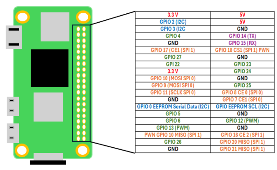
Pinout Diagram
The figure below illustrates the 40‑pin layout. Even though it depicts a Raspberry Pi 4 Model B, the Zero 2 W shares the same header arrangement.
Pins are colour‑coded by function (power, ground, UART, I²C, SPI, PWM and PCM). Use the table above in conjunction with this diagram for accurate wiring.
Applications and Design Examples
Digital Design and Prototyping
Logic level converters – Use the Zero 2 W as a bridge between digital sensors operating at different voltages. For example, interface a 5‑V Arduino to a 3.3‑V sensor through the Pi’s SPI bus and process data locally.
Signal generation – Leverage PWM pins to generate clock signals or control the brightness of LEDs. The hardware PWM outputs provide more precise timing than software bit‑banging.
I²C bus expansion – Connect multiple I²C devices such as ADCs, DACs, real‑time clocks and IO expanders to create modular data acquisition systems.
Embedded Applications
IoT node – With built‑in Wi‑Fi and BLE, the Zero 2 W can serve as a sensor hub sending telemetry to the cloud. Use I²C sensors and MQTT libraries to publish data.
Portable instrumentation – Combine the Pi with a small display, battery and sensors to build a handheld oscilloscope or logic analyser. The 40‑pin header provides access to digital inputs, while SPI can interface with high‑speed ADCs.
Automation and robotics – Use PWM outputs to drive servos or motor drivers. Combine sensor inputs (ultrasonic, accelerometer) and control outputs to build autonomous robots.
Suggested Reading: How Is The Raspberry PI Used In The IIoT?
Education and Experimentation
For electronics students, the Zero 2 W is an affordable platform to learn digital design, bus protocols and embedded Linux. Experiment with:
Breadboarding circuits – Use a Pi Wedge or GPIO breakout board to connect the Pi to a breadboard safely.
Driving displays – Connect SPI‑based OLED displays or I²C character LCDs and write Python scripts to display sensor readings.
Data logging – Use Python to periodically sample analog signals via an external ADC and log data to a micro‑SD card.
Custom hats – Design PCBs that plug into the 40‑pin header, leveraging the ID EEPROM pins for automatic configuration.
Conclusion
The Raspberry Pi Zero 2 W brings significant processing power and connectivity to an exceptionally small single‑board computer. Its 40‑pin header replicates the pinout of the larger Raspberry Pi boards, exposing 26 general‑purpose I/O pins and multiple serial interfaces.
Understanding this pinout is crucial for engineers who wish to interface sensors, actuators and communication peripherals without damaging the board. Designers should observe 3.3‑V logic levels, current limits, and proper numbering schemes, while taking advantage of alternate functions like SPI, I²C, UART, PWM and PCM. When combined with careful power management and thermal considerations, the Zero 2 W becomes a versatile platform for IoT devices, custom hardware, education, and rapid prototyping.
FAQs
1. Can the Zero 2 W be powered via the GPIO header instead of the micro‑USB power port?
Yes. Supplying 5 V directly to pins 2 or 4 and connecting ground to any ground pin will power the board. However, this bypasses the onboard polyfuse and over‑voltage protection, so only use it with a regulated 5 V supply
2. Are the GPIO pins 5‑V tolerant?
No. All GPIOs on the Zero 2 W operate at 3.3 V and are not 5‑V tolerant. Use logic‑level shifters when interfacing with 5‑V devices.
3. How many GPIOs are available for general use?
Out of the 40 pins, 2 are 5‑V, 2 are 3.3‑V, 8 are ground and 2 are reserved for the ID EEPROM. This leaves 26 pins that can function as general‑purpose inputs or outputs.
4. Can I use the Zero 2 W to read analog signals directly?
No. The Raspberry Pi lacks a built‑in ADC. To read analog voltages, connect an external ADC (e.g., MCP3008 via SPI or ADS1115 via I²C) and read its digital outputs using the appropriate bus.
5. What is the difference between physical pin numbering and BCM numbering?
Physical numbering refers to the position of pins on the 2×20 header. BCM numbering identifies the GPIO index within the SoC and is used by software libraries. For example, physical pin 11 is BCM 17.
6. How do I enable I²C or SPI on the Zero 2 W?
Use the raspi-config tool or edit /boot/config.txt. To enable I²C, set dtparam=i2c_arm=on; to enable SPI, set dtparam=spi=on. A reboot is usually required.
7. Does the Zero 2 W support network boot or PoE?
No. The Zero 2 W does not support network boot or power‑over‑Ethernet. It can boot from the micro‑SD card only.
8. Can I use multiple UARTs on the Zero 2 W?
The primary PL011 UART is on GPIO14/15. A secondary mini‑UART can be mapped to other pins via the device tree, but it has limited features. For additional serial ports, use USB‑to‑serial adapters.
References
Raspberry Pi Zero 2 W Product Brief, available at: datasheets.raspberrypi.com
Raspberry Pi official buy page, available at: raspberrypi.com
Cirkit Designer pinout description, available at: docs.cirkitdesigner.com
Pinout.xyz GPIO mapping, available at: pinout.xyz
Random Nerd Tutorials pinout table, available at: randomnerdtutorials.com
Raspberry Pi test pad locations, available at: datasheets.raspberrypi.com
SparkFun learning tutorial on Pi Zero 2 W, available at: learn.sparkfun.com
Waveshare feature summary, available at: waveshare.com