PCB Layout: A Comprehensive Guide
A Printed Circuit Board (PCB) layout is the blueprint that guides the production of circuit boards which are the backbone of any electronic device. This article explores the core principles of PCB layout, component placement, trace routing, signal integrity, and more.

07 Nov, 2023. 15 minutes read
PCB Design Layout
Introduction
The world of electronics design is intricately woven with the art and science of Printed Circuit Board (PCB) layout. PCBs serve as the backbone of countless electronic devices, from smartphones to spacecraft, and the way they are designed and manufactured significantly impacts the performance and reliability of these technological marvels. In this comprehensive exploration, we will unravel the multifaceted realm of PCB layout, shedding light on the vital interplay of solder, PCB manufacturing processes, stack-up configurations, solder mounts, and board layout, as these elements converge to shape efficient and reliable electronic systems.
The layout of a PCB is akin to a meticulously crafted blueprint, providing a comprehensive map that precisely dictates the placement of essential electronic components such as resistors, capacitors, and integrated circuits (ICs). It serves as the architectural canvas where the intricate symphony of electrical connections unfolds. This intricate design blueprint not only governs the locations where these components must reside but also delves into the intricacies of how they harmoniously interact with each other through an intricate network of conductive tracks and pads. These conductive pathways are the lifeblood of any electronic system, transmitting signals and power to ensure the seamless operation of the device.
In essence, a PCB layout is not just a design, but a complex map that guides the functionality of an electronic device. This process demands a profound understanding of electronic components, circuit theory, and design principles. Therefore, the role of a PCB designer is pivotal in the electronics industry. They must possess a strong foundation in electronics, be proficient in PCB design software, and have an acute attention to detail to ensure that the layout is not only accurate but also highly efficient in serving its intended purpose.[1]
The Basics of PCB Design
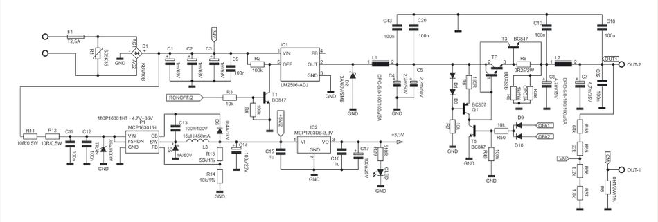
PCB design is a complex process that involves several stages, from conceptualization to final production. It begins with the creation of a schematic diagram, which is a symbolic representation of the circuit. This diagram includes all the components that will be part of the circuit and their interconnections. The schematic serves as the guide for the PCB layout, which is the physical representation of the circuit.
The role of a PCB designer is multifaceted. They are responsible for translating the schematic into a functional PCB layout. This involves deciding the placement of components, routing the interconnections, and ensuring that the design adheres to industry standards and guidelines. The designer must also consider factors such as the electrical requirements of the circuit, the physical constraints of the PCB, and the manufacturing process.[2]
Components of a PCB
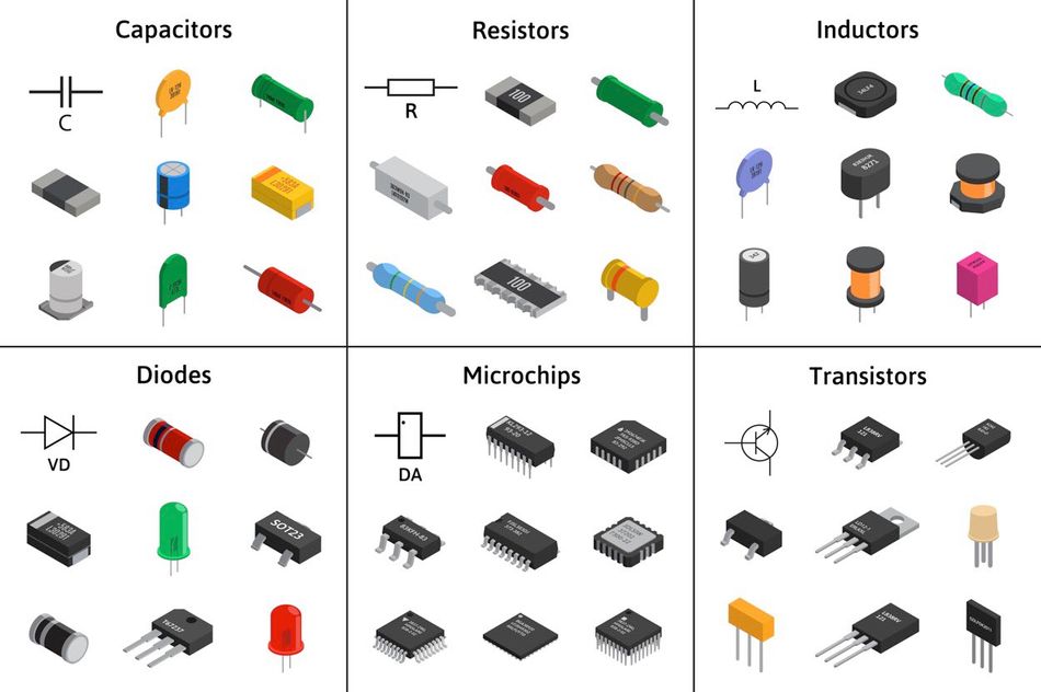
A PCB is composed of several components, each serving a specific function. The primary component is the board itself, which is typically made of non-conductive material like fiberglass or plastic. This board serves as the base upon which other components are mounted.
Resistors are common components found on a PCB. They regulate the flow of electricity through the circuit by providing resistance. The value of a resistor, measured in ohms, determines how much it resists the flow of current.
Capacitors are another type of component. They store and release electrical energy, acting somewhat like a battery. Capacitors are crucial for filtering noise from the power supply, blocking direct current (DC) while allowing alternating current (AC) to pass, and for many other functions.
Integrated Circuits (ICs) are essentially miniaturized circuits themselves that perform specific functions. These can range from simple logic gates to complex microprocessors. ICs are typically the most complex components on a PCB and often dictate the overall functionality of the device. The conductive tracks and pads are what connect all these components. These tracks, often made of copper, are etched onto the board in the design process. They provide the path for electrical current to flow between components. Pads are small portions of exposed metal where components are soldered onto the board. Each of these components plays a crucial role in the overall function of the PCB. The layout and interconnection of these components determine how the circuit performs and how the electronic device operates.[3]
Further reading: Components of a PCB: A Comprehensive Guide
Types of PCBs
PCBs come in various types, each suited to different applications based on their physical and electrical properties.
Single-sided PCBs are the simplest type. They have components on one side of the board and conductive copper tracks on the other. These are typically used in simple electronics where space and complexity aren't significant concerns, such as in power supplies and radios.
Double-sided PCBs have conductive copper tracks on both sides of the board. This allows for a higher density of components and interconnections, making it suitable for more complex devices. The two sides are connected using through-hole technology, where holes are drilled through the board and filled with conductive material to create electrical connections.
Multilayer PCBs take this concept further by having multiple layers of conductive tracks separated by insulation. These can range from 4 to 12 layers, or even more in high-density designs. The layers are connected using vias, similar to double-sided PCBs. Multilayer PCBs are used in highly complex devices like computers and medical equipment, where space is at a premium and a high degree of electrical performance is required.
Rigid PCBs are made from a solid substrate material like fiberglass that keeps its shape. They are durable and can support heavy components, but they can't bend or flex. These are commonly used in desktop computers and other stationary electronics.
Flexible PCBs, in contrast, are made from materials like flexible plastic or Kapton. They can bend and flex without damaging the circuit. This makes them ideal for use in devices like cameras and mobile phones, where the PCB needs to fit into a compact, irregularly shaped casing.
Each type of PCB offers unique advantages and challenges in terms of design, manufacturing, and application. The choice of PCB type depends on the specific requirements of the electronic device being designed, including its complexity, physical constraints, and performance requirements.[4]
Further reading: PCB Layers: Everything You Need to Know
The PCB Layout Process
The process of creating a PCB layout is a multi-step endeavor that requires careful planning and execution. It begins with the creation of a schematic diagram, which is a symbolic representation of the circuit. This diagram includes all the components that will be part of the circuit and their interconnections. The schematic serves as the guide for the PCB layout, which is the physical representation of the circuit.
Once the schematic is complete, the next step is to translate this into a PCB layout. This involves deciding the placement of components, routing the interconnections, and ensuring that the design adheres to industry standards and guidelines. The designer must also consider factors such as the electrical requirements of the circuit, the physical constraints of the PCB, and the manufacturing process.
Schematic Capture
Schematic capture is a pivotal phase in electronic circuit design, representing the art of creating a schematic diagram that serves as the circuit's blueprint. This diagram encompasses all components, complete with their schematic symbols, which are key to understanding their electrical functions and connections. Specialized software simplifies this process, offering designers the means to seamlessly insert and arrange components and draw the all-important connections.
The schematic capture process requires a deep understanding of the circuit's functionality. The designer must know what each component does, how they interact with each other, and how they contribute to the overall function of the circuit. For example, a resistor might be used to limit the current to a safe level for a particular component, while a capacitor might be used to filter out noise from the power supply.
Once the schematic capture is complete, it is then used as the guide for creating the PCB layout. The layout process involves translating the schematic into a physical design, deciding where each component will be placed on the board, and routing the interconnections between them. This requires a careful balance of electrical requirements, physical constraints, and design rules to ensure a functional and manufacturable PCB.[5]
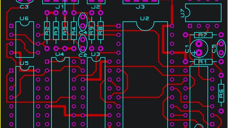
Component Placement
Component placement is a pivotal phase in the PCB layout process, one that demands meticulous attention to detail and adherence to design rules and guidelines. The objective is to create a layout that optimizes electrical efficiency, conserves space, and aligns with design rules, all while harmonizing the integration of surface mount components, Allegro design software, and the intricacies of circuitry.
The placement of components on a PCB is governed by a multitude of factors, each contributing to the overall performance and reliability of the final product. Foremost, the designer must account for the electrical requisites of the circuit. Components sharing a common function or signal path should be thoughtfully grouped, minimizing interconnection lengths. This reduction serves to mitigate signal degradation and electromagnetic interference (EMI), fostering the circuit's integrity.
Thermal management takes center stage in this endeavor. Components that generate substantial heat, such as power transistors and voltage regulators, necessitate strategic placement in areas with ample airflow or proximity to heat sinks. This ensures efficient heat dissipation, safeguarding against overheating and upholding device reliability.
The physical constraints of the PCB and the components themselves also play a part in the component placement. Components with large footprints or that require specific mounting hardware may need to be placed in specific locations on the board. Additionally, components that need to be accessible for maintenance or adjustment, such as connectors or potentiometers, should be placed in easily accessible locations.
Design rules and guidelines, often dictated by industry standards or device-specific parameters, exert their influence. These rules encompass minimum spacing between components, clearance from board edges, and alignment with other components. Strict adherence to these principles guarantees a manufacturable PCB design that meets industry standards.[6]
Routing
Routing is the process of connecting the components on a PCB through conductive tracks. These tracks, often made of copper, provide the path for electrical current to flow between components. Routing is a critical aspect of PCB layout design, as it directly impacts the performance and reliability of the circuit.
When routing a PCB, several factors must be considered. First, the designer must ensure that the routing adheres to the design rules and guidelines. These rules, which can include minimum track width, spacing between tracks, and clearance from board edges, ensure that the PCB can be manufactured reliably and efficiently.
Signal integrity stands as another paramount consideration in the routing phase, playing a pivotal role in the design of high-performance electronic circuits. Designers are tasked with safeguarding the integrity of signals as they traverse the PCB, and in this endeavor, signal layers and signal traces emerge as vital components of the equation. The designer must minimize the length of the tracks and avoid sharp bends, as these can cause signal degradation and increase the risk of electromagnetic interference (EMI). Additionally, high-speed signals and sensitive analog signals should be routed away from noisy components, such as switching power supplies, to minimize the risk of crosstalk and other signal integrity issues.
Power distribution is also a critical aspect of routing. The designer must ensure that the power supply tracks are wide enough to handle the required current and that they are routed efficiently to minimize voltage drops. Ground planes, which are large areas of copper connected to the ground, can be used to provide a low-impedance return path for currents and to improve the overall performance of the circuit.
Thermal management is another factor to consider when routing a PCB. Tracks that carry high currents can generate significant amounts of heat, which can lead to overheating and failure of the device. To mitigate this risk, the designer can use wider tracks, add thermal vias to dissipate heat or route the tracks in a way that maximizes heat dissipation.[7]
PCB Layout Design Rules
Design rules, encompassing track width, spacing, clearance, component placement, layer boards, the number of layers, mils as the measurement unit, and a meticulous step-by-step approach, are vital in the PCB layout process. These guidelines are fundamental for ensuring the manufacturability and electrical performance of the PCB. Adhering to these rules is imperative, as any violations can lead to defects or poor performance. Often rooted in industry standards like IPC, these regulations can be tailored to the specific requirements of the device being designed. The number of layers and their precise stacking, defined in mils, significantly influence the PCB's overall functionality and manufacturability.
Clearance and Creepage
Clearance and creepage are two important design rules related to the spacing between conductive elements on a PCB. Both are critical for ensuring the safety and reliability of the circuit.
Clearance refers to the shortest distance between two conductive elements through air. It is important to maintain adequate clearance to prevent electrical arcing, which can cause damage to the PCB or even lead to a fire. The required clearance depends on factors such as the voltage level of the circuit, the type of insulating material used, and the environmental conditions in which the device will operate.
Creepage is the shortest distance between two conductive elements along the surface of the insulating material. Creepage is important because it helps prevent the formation of conductive paths due to contaminants, moisture, or other factors that can cause a short circuit or leakage current. Like clearance, the required creepage distance depends on the voltage level, insulating material, and environmental conditions.
To ensure the safety and reliability of a PCB, designers must carefully consider clearance and creepage requirements when creating the layout. This involves selecting appropriate insulating materials, maintaining adequate spacing between conductive elements, and accounting for the specific operating conditions of the device. By adhering to clearance and creepage design rules, designers can minimize the risk of electrical failures and ensure the long-term performance of the PCB.[8]
Via Design
Vias are essential in PCB layout, providing electrical connections between layers. They come in various types, such as through-hole, blind, and buried vias. Through-hole vias connect the top and bottom layers, while blind vias connect outer layers to inner layers without passing through the entire board. Buried vias connect inner layers exclusively.
When designing vias, it is essential to consider their size and spacing. The diameter of the via hole and the thickness of the plating can impact the electrical performance and mechanical strength of the connection. Designers must also ensure that vias are spaced far enough apart to avoid short circuits and to meet the manufacturing tolerances of the PCB fabrication process.
Thermal management is another critical aspect of via design. Vias can help dissipate heat generated by components, especially in multi-layer PCBs. Designers can use thermal vias, which are strategically placed to improve heat transfer between layers and to external heat sinks or thermal pads.
Further reading: What is a Via: A Comprehensive Guide
PCB Layout Software
PCB layout software is a critical tool in the design and creation of printed circuit boards. It allows engineers to design and visualize the layout of a PCB, including the placement of components and routing of traces. The software also includes features for checking design rules, simulating circuit performance, and generating files for manufacturing.
One of the key features of PCB layout software is the ability to create and manage a library of components. This library includes the physical dimensions, pin configurations, and other specifications of each component. The software can automatically place these components on the PCB layout, ensuring accurate alignment and spacing.
Another important feature is the routing of traces. The software can automatically route traces between components based on the schematic diagram while adhering to design rules such as minimum trace width and clearance. The software can also highlight areas of potential interference or violation of design rules, allowing the designer to make necessary adjustments.
The software also includes simulation tools that can predict the performance of the circuit. These tools can simulate the flow of current, the propagation of signals, and the generation of heat. This allows the designer to identify and address potential issues before the PCB is manufactured.
Finally, the software generates files that can be used for manufacturing the PCB. These files include the Gerber files, which specify the layout of the traces and components, and the drill files, which specify the locations of holes for through-hole components and vias.[9]
CAD Tools for PCB Layout
Computer-aided design (CAD) tools are specialized software for PCB layout, offering advanced capabilities for designing and simulating PCBs. They enable precise control over component and trace placement, along with robust simulation features for circuit behavior analysis. Key CAD tool features encompass 3D PCB modeling for enhanced visualization and issue identification, as well as support for mechanical design.
Advanced simulations aid in optimizing performance and reliability by assessing circuit behavior under various conditions like temperature, voltage, and frequency variations. CAD tools also offer sophisticated routing features, automating complex trace patterns and multi-layer routing to enhance signal integrity and performance.
Additionally, CAD tools generate detailed manufacturing files, including Gerber files, drill files, and assembly drawings, ensuring precise instructions for accurate PCB production.
Simulation Tools
Simulation tools play a crucial role in the PCB design process, allowing designers to predict the performance of their circuits and identify potential issues before manufacturing. These tools can simulate various aspects of the circuit, such as signal integrity, power distribution, and thermal performance.
Signal integrity simulations help designers analyze the quality of signals transmitted through the PCB traces. These simulations can identify issues such as reflections, crosstalk, and signal attenuation, which can degrade the performance of high-speed digital circuits. By identifying these issues early in the design process, designers can make necessary adjustments to the layout, trace routing, and termination strategies to ensure optimal signal integrity.
Power distribution simulations focus on analyzing the voltage and current distribution across the PCB. These simulations can identify areas of high current density, voltage drops, and potential hotspots that may lead to thermal issues or component failures. By optimizing the power distribution network, designers can improve the overall efficiency and reliability of the circuit.
Thermal simulations are essential for predicting the temperature distribution across the PCB and identifying potential hotspots that may cause component failures or reduce the lifespan of the board. These simulations take into account factors such as component power dissipation, heat transfer mechanisms, and ambient temperature conditions. By identifying areas of high temperature, designers can make adjustments to the layout, such as increasing trace widths, adding thermal vias, or improving heat dissipation through the use of heat sinks or thermal pads.
Simulation tools often integrate with PCB layout software, allowing designers to perform simulations directly within the design environment. This seamless integration enables designers to quickly iterate on their designs and make necessary adjustments based on the simulation results. Some popular simulation tools include SPICE (Simulation Program with Integrated Circuit Emphasis), HyperLynx by Mentor Graphics, and Ansys SIwave. These tools offer a range of simulation capabilities, catering to the needs of various design complexities and requirements.[10]
Challenges in PCB Layout Design
Designing a PCB layout can be a complex and challenging process, with numerous factors to consider and potential pitfalls to avoid. Some of the key challenges faced by designers include:
Component placement
The arrangement of components on the PCB can have a significant impact on the performance and reliability of the circuit. Designers must consider factors such as signal integrity, thermal management, and electromagnetic interference when placing components. Additionally, designers must ensure that components are placed in a manner that allows for efficient routing of traces and minimizes the overall board size.
Signal integrity
High-speed signals can be susceptible to degradation due to factors such as reflections, crosstalk, and signal attenuation. Designers must carefully consider the routing of traces, the use of termination strategies, and the selection of appropriate materials to maintain signal integrity throughout the PCB.
Thermal management
Heat dissipation is a critical aspect of PCB design, as excessive temperatures can lead to component failures and reduced board lifespan. Designers must consider the power dissipation of components, the use of thermal vias, and the incorporation of heat sinks or thermal pads to manage heat effectively.
Electromagnetic interference (EMI)
EMI can cause unwanted noise and signal degradation in a PCB. Designers must take steps to minimize EMI by carefully routing traces, using shielding techniques, and ensuring proper grounding.
Design for manufacturability (DFM)
A successful PCB design must be manufacturable, meaning it can be produced efficiently and cost-effectively. Designers must consider factors such as trace widths, via sizes, and component tolerances to ensure that the PCB can be manufactured without issues.
Design rule checking (DRC)
Ensuring that a PCB design adheres to established design rules is crucial for avoiding manufacturing issues and ensuring reliable performance. Designers must use DRC tools to identify and correct any violations of design rules before the PCB is manufactured.
Collaboration and communication
PCB design often involves collaboration between multiple team members, including electrical engineers, mechanical engineers, and manufacturing specialists. Effective communication and collaboration are essential for ensuring that all aspects of the design are considered and that potential issues are identified and addressed early in the process.
Conclusion
PCB layout is the design phase that precedes PCB manufacturing. The design is complex and challenging, and it requires careful consideration of various factors, including component placement, signal integrity, thermal management, and electromagnetic interference. The quality of the PCB layout design directly affects the quality and functionality of the manufactured printed circuit board. Designers must therefore ensure that their designs are manufacturable and adhere to established design rules.
The use of PCB layout software, CAD tools, and simulation tools can greatly assist designers in overcoming these challenges and creating high-quality, reliable PCBs. By understanding the key concepts and challenges involved in PCB layout design, designers can develop the skills and expertise needed to create successful and efficient PCBs. Close collaboration and communication between PCB designers and manufacturers are crucial to achieving a successful and reliable PCB product.
FAQs
What is the importance of component placement in PCB layout design?
Component placement is crucial for the performance and reliability of a circuit. Proper placement ensures efficient routing of traces, minimizes board size and helps manage signal integrity, thermal management, and electromagnetic interference.How can simulation tools help in PCB layout design?
Simulation tools can predict the performance of a circuit and identify potential issues before manufacturing. They can simulate various aspects of the circuit, such as signal integrity, power distribution, and thermal performance, allowing designers to optimize their designs.What are some challenges faced by designers in PCB layout design?
Some key challenges include component placement, signal integrity, thermal management, electromagnetic interference, design for manufacturability, design rule checking, multi-layer PCBs, and collaboration and communication among team members.What is the role of CAD tools in PCB layout design?
CAD tools provide advanced features for designing and simulating PCBs, allowing for more precise control over the layout and routing of components and traces. They also include advanced simulation features that can model the behavior of the circuit under various conditions.Why is thermal management important in PCB layout design?
Thermal management is essential for preventing component failures and reducing the lifespan of the board. Designers must consider factors such as component power dissipation, heat transfer mechanisms, and ambient temperature conditions to ensure effective heat dissipation and avoid potential hotspots.
Reference
Utmel Electronics, 2020. Introduction to PCB Layout Principles. Available at: https://www.utmel.com/blog/categories/pcb/introduction-to-pcb-layout-principles (Accessed: November 3, 2023).
Sierra Circuits, 2021. Mastering the art of PCB Design Basics. Available at: https://www.protoexpress.com/blog/mastering-pcb-design-basics/#:~:text=Printed%20circuit%20board%20design%20begins,the%20traces%20on%20the%20board.(Accessed: November 3, 2023).
Abiola Ayodele (Wevolver), 2023. Components of a PCB: A Comprehensive Guide. Available at: https://www.wevolver.com/article/components-of-a-pcb-a-comprehensive-guide (Accessed: November 3, 2023).
World Electronics, 2021. Types of Printed Circuit Boards. Available at: https://worldsway.com/types-of-pcb-boards/ (Accessed: November 3, 2023).
Jessica Miley (Wevolver), 2020. The Printed Circuit Board Design and Manufacturing Cycle: Symbiotic Relationships Engage Innovation. Available at: https://www.wevolver.com/article/the-printed-circuit-board-design-and-manufacturing-cycle-symbiotic-relationships-engage-innovation (Accessed: November 3, 2023).
Proto-electronics, 2022. Best Rules for PCB Components Placement. Available at: https://www.google.com/amp/s/www.proto-electronics.com/blog/best-rules-for-pcb-components-placement%3fhs_amp=true (Accessed: November 4, 2023).
RAYPCB, 2023. What is PCB Routing.? Available at: https://www.raypcb.com/pcb-routing/#:~:text=Routing%20is%20the%20process%20of,signal%20integrity%20and%20electromagnetic%20compatibility. (Accessed: November 4, 2023).
CTC, 2020. What is clearance and creepage distance of insulation? Available at: https://www.powerctc.com/en/node/4757 (Accessed: November 4, 2023).
G2, 2023. Best PCB Design Software. Available at: https://www.g2.com/categories/pcb-design (Accessed: November 4, 2023).
Zachariah Peterson, 2020. Circuit CAD Software for PCB Design. Available at: https://resources.altium.com/p/cad-software-for-pcb-design (Accessed: November 5, 2023).