Crystalline vs Amorphous: Structure, Properties and Engineering Implications
This article is a detailed exploration of crystalline vs amorphous solids, covering atomic order, materials properties, semiconductors, and how they translate into practical semiconductor, hardware and digital design applications.

12 Sep, 2025. 17 minutes read
Introduction
In materials science, the comparison of crystalline vs amorphous structures is fundamental to understanding how atomic arrangement influences physical and engineering properties. The crystalline solids are characterized by a highly ordered lattice structure, where atoms are arranged in repeating patterns that extend in three dimensions. In contrast, amorphous materials lack long-range order, exhibiting random atomic arrangements that result in different mechanical, optical, and thermal behaviors.
The debate, crystalline vs amorphous, carries practical implications across industries, from electronics and semiconductors to construction and biomaterials. For example, crystalline silicon is the backbone of microelectronics, while amorphous silicon finds applications in thin-film solar cells. Similarly, crystalline metals exhibit predictable strength and ductility, whereas amorphous alloys (metallic glasses) offer unique corrosion resistance and hardness.
By exploring crystalline vs amorphous structures, properties, and applications, engineers and researchers gain critical insights into material selection, performance optimization, and innovation in advanced technologies.
Understanding the Atomic Structure
Ordered Lattices and Long-Range Periodicity
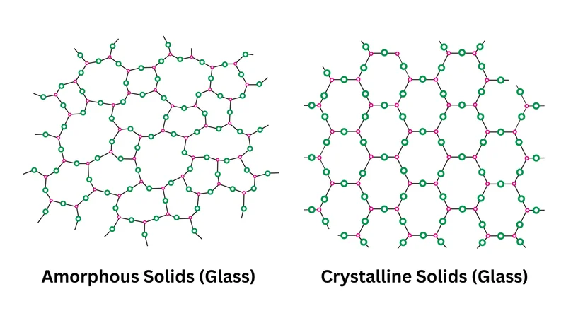
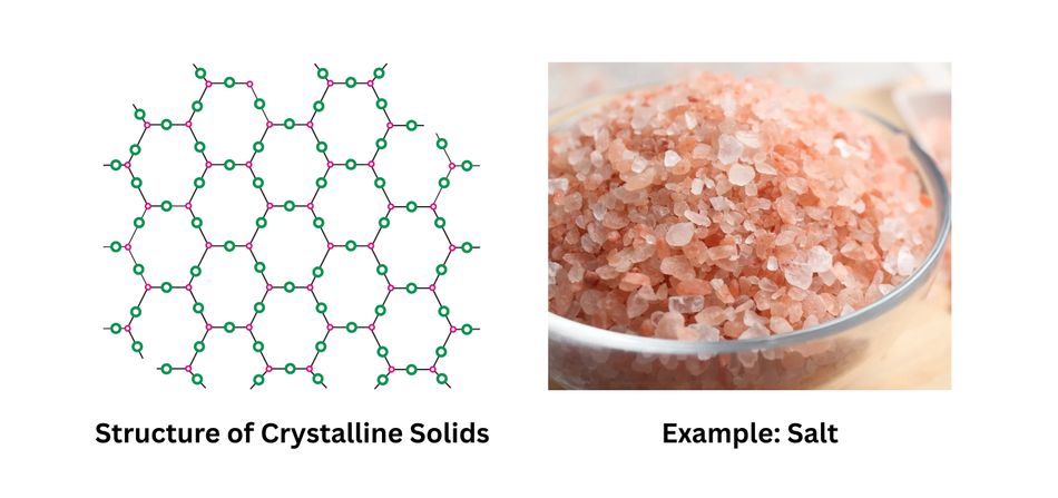
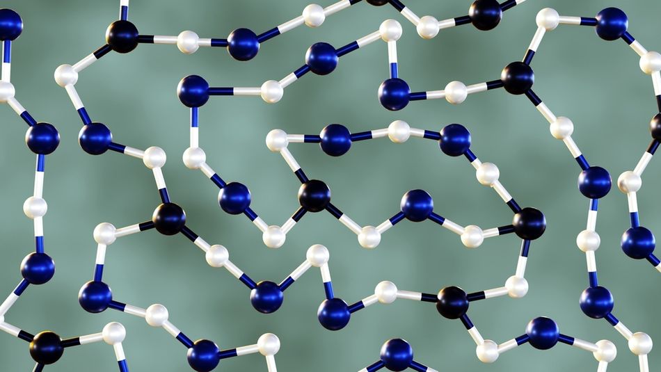
In crystalline solids, atoms are arranged in a repeating, highly ordered pattern known as a lattice. Each atom occupies a fixed position in a unit cell, which is the fundamental building block of the crystal structure. This periodic arrangement extends across three dimensions, resulting in long-range order. Materials such as metals, salts, and semiconductors exhibit this characteristic.
The presence of an ordered lattice directly influences the physical appearance and functional properties of crystalline materials. For example, crystals often form distinct geometric shapes with well-defined facets, reflecting their underlying atomic arrangement. Moreover, properties such as electrical conductivity, optical behavior, and mechanical strength vary with crystallographic direction, a phenomenon known as anisotropy. [1] This explains why a single material, like quartz, can behave differently depending on orientation.
The sharp melting point is another hallmark of crystalline solids. When heated, the lattice structure collapses abruptly at a specific temperature, requiring the absorption of a precise heat of fusion before transitioning to the liquid state.
Disordered Networks and Short-Range Order
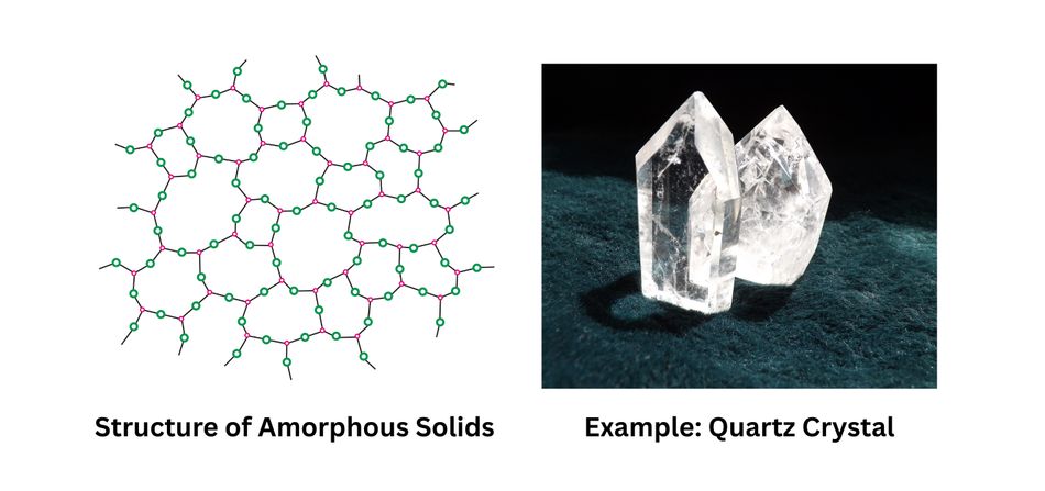
By contrast, amorphous solids lack long-range periodicity. Instead of an extended lattice, atoms or molecules are distributed randomly, with only short-range order preserved. So, the immediate neighbors of an atom remain relatively fixed, but the organization does not extend further. The common examples include glasses, polymers, gels, and amorphous silicon thin films.
This absence of long-range order results in isotropic behavior, where properties such as refractive index, elastic modulus, and electrical conductivity are uniform in every direction. Unlike crystalline solids, amorphous materials do not exhibit a sharp melting point. Instead, they soften gradually over a range of temperatures, transitioning from a rigid state to a viscous one. This unique thermal response makes them highly versatile in processing and fabrication techniques, such as glass blowing, thin-film deposition, and molding of polymer components.
In addition, the ability to fine-tune amorphous structures through additives or heat treatment offers engineers flexibility in customizing mechanical strength, optical transparency, or chemical resistance for specific applications.
Summary of Structural Differences
| Property | Crystalline Solids | Amorphous Solids |
| Atomic Arrangement | Long Range Periodic Lattice | Random Network with Short Range Order |
| Symmetry | Anisotropic | Isotropic |
| Melting Behaviour | Sharp Melting Point and Definite Heat of Fusion | No Definite Heat of Fusion |
| Cleavage | Cleaves along Well Defined Planes | Fractures with Irregular Surfaces |
| Rigidity | Strong (Ductile) | Pseudo Solids with Partial Fluidity |
| Chemical Reactivity | Low | High |
| Examples | Metals, Salts, Minerals, Crystalline Silicon | Glass, Polymers, Amorphous Silicon, Metallic Glasses |
The structural contrast between crystalline and amorphous solids highlights their mechanical, thermal, optical, and electronic properties. It becomes easier for engineers to choose one over the other in design and manufacturing: crystalline silicon, with its ordered lattice, dominates semiconductor technology, while amorphous silicon is preferred in flexible thin-film solar cells.
Similarly, the rigidity of crystalline metals enables high-strength structural applications, whereas the formability and isotropic nature of amorphous materials make them indispensable in optics, coatings, and polymer engineering.
Recommended Reading: Reliable, Scalable, Anisotropic Interconnect Solution for Wearable Electronics
Physical Properties: Mechanical, Thermal, and Optical
Mechanical Strength and Elasticity
The mechanical response of a solid is strongly influenced by its atomic arrangement. In crystalline metals, plastic deformation typically occurs through the movement of dislocations, line defects in the crystal lattice that act as slip pathways under stress. While this allows metals to deform without catastrophic failure, it also limits their ultimate strength. Strengthening mechanisms such as alloying, grain refinement, and work hardening are therefore commonly employed to restrict dislocation motion and improve performance.
In contrast, amorphous metals, also known as metallic glasses, possess no long-range lattice order and consequently lack traditional dislocation mechanisms and grain boundaries. This homogeneous structure results in exceptional tensile strength and elastic strain capacity, often surpassing that of crystalline alloys. For instance, the amorphous alloy Vitreloy 1 exhibits tensile strengths approaching 1.9 GPa, nearly double that of high-strength steels. [2] It can sustain elastic strains of ~2%, compared with only about 0.2% in crystalline metals. Furthermore, the absence of grain boundaries provides enhanced corrosion resistance, as these interfaces are common initiation sites for localized corrosion in crystalline metals.
Despite these advantages, amorphous metals also have limitations. Their disordered structure makes them inherently brittle, particularly under tensile loading, and they are challenging to manufacture in bulk. To avoid crystallization during solidification, extremely rapid cooling rates, sometimes exceeding 10⁶ K/s, are necessary. In contrast, crystalline metals are relatively easy to process, weld, and fabricate into large components. They also exhibit tunable properties through well-established metallurgical techniques.
For engineers, the choice between crystalline and amorphous metals depends on the application: amorphous alloys are preferred in high-performance precision components, transformer cores, and corrosion-resistant coatings, while crystalline alloys dominate structural, automotive, and aerospace engineering due to scalability and ductility.
Thermal Behavior
Thermal characteristics also differ significantly between crystalline and amorphous solids. The crystalline materials display well-defined melting points, where the lattice abruptly collapses into a liquid. For example, pure crystalline silicon melts sharply at 1,414 °C, with a distinct heat of fusion. This predictability makes crystalline materials suitable for processes requiring precise thermal control, such as soldering, crystal growth, and semiconductor fabrication.
In contrast, amorphous solids lack a sharp melting point. Instead, they undergo a gradual transition across a glass-transition temperature (Tg), where the material shifts from a brittle, glassy state to a ductile or viscous form. Common examples include glass and polymers, which soften progressively as they approach Tg, allowing them to be shaped through thermoforming, blow molding, or thin-film deposition. While the absence of a precise melting point complicates applications requiring exact melting, it enables greater flexibility in forming processes.
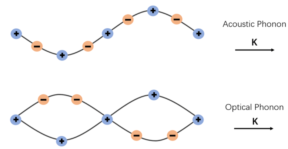
Thermal conductivity further differentiates the two classes! In crystalline solids, the periodic lattice enables phonons (quantized lattice vibrations) to travel efficiently, resulting in higher thermal conductivity. Diamond and crystalline silicon are well-known for their outstanding heat conduction, which is critical in electronics and high-power devices.
In contrast, the random structure of amorphous solids scatters phonons, lowering thermal conductivity. This property is exploited in thermal insulators, glass wool, and even thermal barrier coatings in turbine blades, as well as in electronics, where localized heating must be contained.
Optical Properties
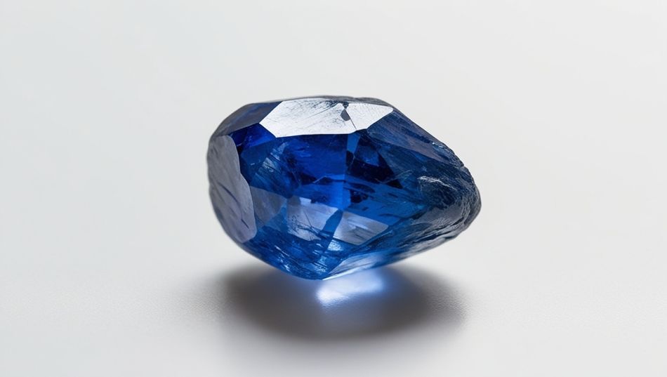
The optical response of crystalline and amorphous materials is likewise determined by their internal order. The crystalline solids often display anisotropic optical properties, meaning that light interacts differently depending on the crystallographic direction. Birefringence in quartz or sapphire is one classic example, where a single light beam splits into two rays with different velocities and refractive indices. This directional dependence is valuable in polarizing optics, photonics, and precision instruments.
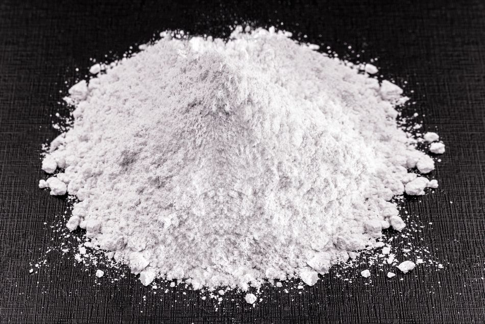
Amorphous materials, by contrast, are generally optically isotropic, with uniform refractive properties in all directions. Glass, the most widely used amorphous solid, is prized for its clarity, transparency, and isotropy, making it indispensable in lenses, optical fibers, and architectural applications. [3]
In semiconductors, structural disorder plays a critical role! The crystalline silicon has a narrow band gap of 1.7 eV due to the presence of localized states in the band structure. This wider gap shifts the absorption edge to higher energies, enabling amorphous silicon to absorb a greater portion of the visible spectrum per unit thickness. It is well-suited for thin-film photovoltaic cells, liquid crystal displays, and photodiodes, even though its carrier mobility is lower compared with crystalline silicon.
Recommended Reading: Glass Transition Temperature of Polymers
Electronic Properties and Semiconductors
Band Structure and Density of States
The electronic properties of crystalline and amorphous semiconductors are fundamentally shaped by their atomic arrangement. In crystalline semiconductors, atoms are organized in a periodic lattice, giving rise to a well-defined band structure with distinct valence and conduction bands separated by a band gap. The periodic potential allows electrons and holes to move efficiently, resulting in high carrier mobility. Doping introduces controlled donor or acceptor states near the band edges, enabling precise tuning of electrical conductivity. This tunability, combined with the formation of a stable native oxide (SiO₂), explains why crystalline silicon remains the backbone of modern integrated circuits and CMOS devices, where predictable and repeatable performance is essential.
In contrast, amorphous semiconductors lack long-range periodicity. The absence of translational symmetry leads to a broadened density of states, with localized “tail states” extending into the band gap. These localized states act as traps for charge carriers, drastically reducing mobility. For example, in amorphous silicon, electrons travel at roughly one-thousandth the speed compared to single-crystal silicon. Doping is also far less effective: the Fermi level tends to become pinned near the mid-gap, since the localized states neutralize added carriers. Consequently, amorphous semiconductors generally exhibit lower mobility, higher resistivity, and less predictable electrical behavior compared to their crystalline counterparts.
Processing and Engineering Implications
Despite these disadvantages, amorphous semiconductors possess unique processing advantages. They can be deposited at low temperatures (<350 °C) using cost-effective techniques such as plasma-enhanced chemical vapor deposition (PECVD). Unlike crystalline semiconductors, they do not require expensive single-crystal wafers. They can instead be deposited onto large-area, low-cost substrates such as glass, metal foils, or even flexible plastics. This scalability makes them highly attractive for large-area electronics where ultra-high performance is not the primary requirement.
For instance, amorphous silicon thin films are widely used in flat-panel displays, thin-film transistors (TFTs), solar cells, and image sensors, where the key priorities are manufacturability, cost-efficiency, and coverage of large surfaces. By contrast, crystalline semiconductors dominate applications requiring high-speed switching, low power consumption, and miniaturization, such as microprocessors, power electronics, and advanced communication systems.
Recommended Reading: What is a Semiconductor? Comprehensive Guide to Engineering Principles and Applications
Crystalline vs Amorphous Silicon in Electronics
Integrated Circuits
In advanced microelectronics, single-crystal silicon remains the undisputed foundation of integrated circuits. Its perfectly ordered lattice supports high carrier mobilities, approximately 1,400 cm²/V·s for electrons and 450 cm²/V·s for holes, allowing transistors to switch at high speeds while consuming minimal power. Equally important is the ability to engineer precise doping profiles, enabling n- and p-type regions with nanometer accuracy. Combined with the formation of high-quality silicon dioxide (SiO₂) gate dielectrics, these attributes have allowed the seamless integration of billions of CMOS transistors onto a single chip.
While polycrystalline silicon finds utility in gate electrodes, interconnects, and passivation layers, the active regions of CMOS devices must be single crystal to deliver the required mobility, reliability, and uniformity. Any deviation from crystallinity would lead to reduced performance, higher leakage, and unacceptable variability in logic and memory devices.
Thin Film Transistors and Displays
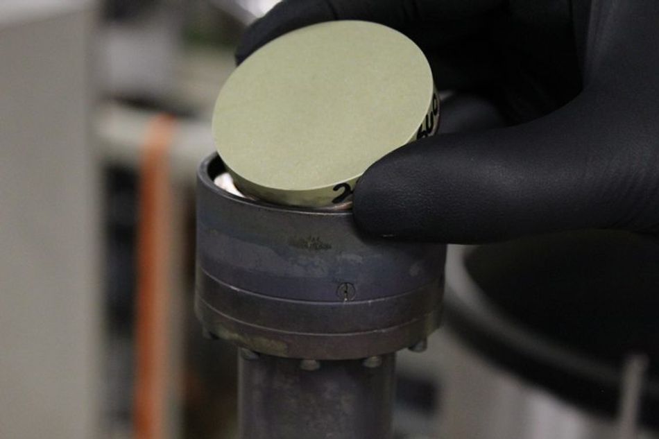
For large-area electronics, such as LCD panels, solar modules, and e-paper displays, the economics of using single-crystal wafers are prohibitive. Instead, amorphous silicon (a-Si) is widely adopted. Deposited as thin films (<1 μm) via plasma-enhanced chemical vapor deposition (PECVD) at relatively low temperatures (250–350 °C), amorphous silicon forms smooth, uniform coatings that can be applied to substrates spanning square meters of glass at low cost.
Unlike polycrystalline films, which contain grain boundaries that act as pathways for impurities and moisture infiltration, amorphous silicon is free from such extended defects, improving film uniformity and reliability. For display applications, a-Si thin-film transistors (TFTs) are sufficient because each pixel requires only moderate switching speeds. However, the intrinsic low mobility (~0.5 cm²/V·s) of a-Si imposes limits on refresh rates and pixel densities. As consumer demand shifted toward HDTVs, OLEDs, and high-refresh-rate monitors, the limitations of a-Si became increasingly problematic, prompting the search for higher-mobility alternatives.
Amorphous Oxide Semiconductors
The limitations of a-Si paved the way for amorphous oxide semiconductors (AOS), such as indium gallium zinc oxide (IGZO) and zinc tin oxide (ZTO). These materials combine the low-cost, large-area processing advantages of amorphous films with much higher carrier mobilities. Electrons in AOS devices typically exhibit mobilities between 10 – 20 cm²/V·s, nearly 40 times greater than in a-Si TFTs. [4] This performance boost arises because electrons in metal oxides occupy large, spherical s-orbitals, which overlap effectively even in disordered structures.
Such improvements enable AOS TFTs to support high refresh rates, enhanced pixel density, and superior power efficiency, making them the preferred technology in next-generation LCD and OLED displays. Furthermore, AOS films can be processed at very low temperatures (<100 °C), enabling deposition on flexible plastic substrates. This capability is critical for the emerging market of flexible, rollable, and transparent electronics.
Research also highlights that AOS materials can achieve mobilities up to 50 cm²/V·s under optimized conditions. Their high ionicity and the broad availability of unoccupied metal s-orbitals create band structures particularly well-suited for n-channel thin-film transistors (TFTs). With these properties, AOS technologies are expected not only to replace a-Si in displays but also to expand into wearable devices, transparent circuits, and flexible sensors.
Recommended Reading: Thin Film Deposition: Everything You Need to Know
Emerging Applications in Advanced Electronics and Materials
Phase-Change Memory and Neuromorphic Computing
One of the most exciting frontiers for crystalline vs amorphous transformations lies in phase-change memory (PCM). This technology leverages the ability of certain chalcogenide alloys (e.g., Ge₂Sb₂Te₅) to reversibly switch between crystalline and amorphous forms under rapid heating and cooling cycles. By applying short electrical pulses, the material can be toggled between a low-resistance crystalline state (logical “1”) and a high-resistance amorphous state (logical “0”). The sharp contrast in resistivity arises because the ordered structure of the crystal lattice promotes efficient electron transport, while the disordered arrangement of atoms in the amorphous form scatters carriers and hinders conductivity.
PCM devices demonstrate remarkable switching speeds in the nanosecond regime, combined with ultra-low power operation and cycling endurance exceeding millions of write/erase events. Unlike traditional flash memory, PCM scales effectively to sub-10 nm dimensions while retaining high reliability. Importantly, engineers can also exploit partial crystallization states, creating intermediate resistance levels that encode analog conductance. This property makes PCM highly attractive for neuromorphic computing architectures, where memory cells mimic biological synapses by storing synaptic weights as varying conductance values. By integrating logic and storage into the same material platform, PCM reduces data transfer bottlenecks and energy consumption, opening the door to next-generation high-efficiency computing.
Amorphous Metals and Magnetic Applications
Amorphous materials are also revolutionizing fields well beyond semiconductors. In electrical power systems, amorphous iron-based alloys are increasingly used in transformer and inductor cores. Their lack of grain boundaries eliminates common dislocation pathways and reduces magnetic coercivity, resulting in dramatically lower core losses compared with crystalline iron. Industry data indicates that transformers built with amorphous cores can deliver up to 70% energy savings, a breakthrough that directly impacts grid efficiency and sustainability.
The advantages of amorphous metals extend to their mechanical and chemical properties as well. With tensile strengths far exceeding those of many crystalline alloys and superior corrosion resistance, they are finding applications in biomedical implants, surgical tools, and aerospace components where reliability under extreme conditions is essential. Sporting goods manufacturers are also experimenting with metallic glasses to create lighter, stronger equipment with excellent durability.
However, engineering challenges remain. The production of bulk amorphous metals requires extremely rapid cooling rates to prevent crystallization, limiting scalability. Additionally, while these materials are strong, they often display intrinsic brittleness, which restricts their use in applications demanding significant plastic deformation. Engineers must carefully balance cost, manufacturability, component size, and mechanical performance when specifying amorphous metals for industrial use.
Characterization and Analytical Techniques
Understanding whether a material is crystalline or amorphous and evaluating its internal structure and physical properties requires a suite of analytical methods. The key techniques include:
X-Ray Diffraction (XRD): Crystalline materials produce sharp, well-defined diffraction patterns because the crystal lattice acts as a periodic grating. Amorphous solids, lacking long-range order, instead yield broad, diffuse scattering. XRD is widely used to identify phases, quantify crystallinity, and measure lattice parameters.
Electron Backscatter Diffraction (EBSD): Provides orientation maps of grains and grain boundaries in crystalline materials, offering complementary microstructural insights alongside XRD.
Raman and Infrared Spectroscopy: Sensitive to bonding and short-range order. Disorder broadens vibrational modes, while peak shifts and intensity changes reveal details of the molecular structure and degree of amorphousness.
Transmission Electron Microscopy (TEM): High-resolution TEM enables direct imaging of the arrangement of atoms, clearly distinguishing amorphous regions from crystalline domains.
X-Ray Absorption Spectroscopy (XAS): Used in phase-change material studies, in-situ high-temperature XAS probes coordination numbers and local electronic environments in both crystalline and amorphous states.
Differential Scanning Calorimetry (DSC): Detects glass transition temperature (Tg), sharp melting point, and crystallization events by measuring heat flow, providing insights into phase transitions and heat of fusion.
Dynamic Mechanical Analysis (DMA): Measures mechanical modulus across a range of temperatures, identifying transitions such as Tg in amorphous polymers and revealing differences in elasticity between crystalline vs amorphous states.
Nuclear Magnetic Resonance (NMR) Spectroscopy: Probes local chemical and electronic environments, helping differentiate ordered structure from disordered arrangements in glasses, polymers, and ceramics.
Small-Angle X-Ray Scattering (SAXS): Sensitive to nanoscale heterogeneity, making it useful for studying semi-crystalline polymers and nanostructured thin films.
Fourier-Transform Infrared Spectroscopy (FTIR): Provides information about functional groups, bonding, and intermolecular forces, particularly valuable in distinguishing amorphous form from crystalline form in organic and polymeric solids.
Atomic Force Microscopy (AFM): Measures surface topography and mechanical stiffness at the nanoscale, revealing differences between smooth amorphous thin films and faceted crystalline surfaces.
Ellipsometry: Determines optical constants and film thickness, commonly applied to thin films of amorphous and crystalline silicon in semiconductor and photovoltaic applications.
X-Ray Photoelectron Spectroscopy (XPS): Provides chemical composition and bonding information, complementing structural analyses by highlighting surface chemistry differences between amorphous and crystalline materials.
These characterization techniques provide critical insights into atomic order and disorder. By combining structural, thermal, and optical methods, engineers can optimize crystalline vs amorphous materials for advanced applications.
Practical Considerations for Engineers
Choosing Between Crystalline and Amorphous Materials
When selecting materials for a given hardware application, engineers should consider:
Performance Requirements: For high‑speed, low‑power logic, crystalline semiconductors are necessary because they offer high mobility and reliable doping. For large‑area, low‑cost displays where switching speeds are modest, amorphous or amorphous oxide semiconductors suffice.
Processing Temperature and Substrate Compatibility: Amorphous materials often allow low‑temperature deposition, enabling use on plastic or glass substrates. Crystalline materials frequently require high temperatures or specialized substrates.
Cost and Scalability: Producing single‑crystal wafers is expensive and limited in size. Amorphous films can be sputtered over meter‑scale substrates, lowering the cost per unit area.
Mechanical and Thermal Properties: For structural components requiring high strength and elasticity, amorphous metals may offer advantages, but brittleness and fabrication limits must be addressed.
Stability and Reliability: Crystalline materials typically have fewer metastable states and better long‑term stability. Amorphous semiconductors can suffer from threshold voltage drift and aging, although new compositions like IGZO mitigate these issues.
Design guidelines
Match Mobility to Circuit Requirements: Use crystalline silicon or high‑mobility oxides for high‑speed transistors; amorphous silicon suffices for low‑frequency switching.
Leverage Amorphous Materials for Large‑Area Electronics: For displays, sensors and photovoltaics, the ability to deposit uniform films on glass or plastic can outweigh mobility drawbacks.
Consider Thermal Budgets: When integrating electronics onto flexible substrates, choose materials (e.g., amorphous oxides) that can be processed at low temperatures (<150 °C) to avoid damaging the substrate.
Utilize Phase Transitions: Where non‑volatile memory or neuromorphic functionality is required, phase‑change materials provide a way to exploit the large resistivity contrast between crystalline and amorphous phases.
Evaluate Mechanical Requirements: For components subject to cyclic loads or requiring high elasticity, amorphous metals may be ideal; however, verify size and cost constraints.
Thoughtful selection ensures reliable, efficient designs tailored to application needs across electronics, energy, and structural systems.
Case Studies
1. Thin-Film Transistor (TFT) Displays
Active-matrix liquid crystal displays (AMLCDs) rely on a thin-film transistor (TFT) to control each pixel independently. Historically, hydrogenated amorphous silicon (a-Si: H) was the preferred channel material because it can be deposited at around 300 °C on inexpensive glass substrates, forming uniform thin films over very large areas. This compatibility with glass enabled the mass production of affordable flat-panel displays.
However, as display resolution, refresh rates, and pixel densities increased, the low electron mobility of a-Si: H (~0.5 cm²/V·s) became a performance bottleneck. [5] Engineers responded by adopting amorphous oxide semiconductors (AOS) such as indium gallium zinc oxide (IGZO), which provide mobilities more than ten times higher than a-Si: H. In addition, IGZO films can be deposited at even lower temperatures, extending substrate compatibility and reducing energy costs. Today, IGZO TFTs underpin high-definition televisions, tablets, and smartphones, delivering faster refresh rates, improved brightness, and enhanced power efficiency.
2. Flexible Electronics
The advent of wearables, foldable displays, and conformal sensors created demand for electronics that can operate on plastic substrates. Traditional amorphous silicon degrades when deposited at the low temperatures (<200 °C) required for plastics. By contrast, amorphous oxide TFTs can be deposited near room temperature and stabilized with mild annealing (250–300 °C). This process retains high mobility and long-term device stability, even on flexible substrates.
The result is a new generation of rollable e-paper, bendable OLED panels, and lightweight medical devices that integrate seamlessly with curved or wearable surfaces. These case studies highlight how processing temperature, substrate compatibility, and isotropic film uniformity drive the adoption of amorphous over crystalline semiconductors in next-generation consumer and biomedical electronics.
3. Phase-Change Memory (PCM)
Phase-change memory (PCM) demonstrates a direct exploitation of reversible crystalline vs amorphous transitions in chalcogenide alloys such as Ge₂Sb₂Te₅. Write operations involve applying short electrical pulses that locally melt and rapidly quench the material, trapping it in the amorphous, high-resistivity state. Reading the cell requires only a low-voltage probe of its resistance. A subsequent heating pulse recrystallizes the material into its low-resistance crystalline state, completing the reversible cycle.
PCM offers nanosecond-scale switching, low operating power, and scalability down to sub-10 nm nodes, outperforming flash memory in both endurance and access time. Importantly, engineers can exploit intermediate resistance states—partial crystallization levels that enable multi-bit storage per cell and even neuromorphic computing, where gradual conductance variations mimic synaptic weights. While challenges remain in thermal management and long-term cycling reliability, PCM represents a paradigm shift in non-volatile, high-bandwidth memory technologies.
4. Transformers and Inductors
In electric power systems, magnetic cores are essential for concentrating magnetic flux in transformers and inductors. Traditional cores are made from crystalline silicon steels, but these suffer from eddy current and hysteresis losses, reducing overall efficiency. The development of amorphous metal cores, typically iron–boron or iron–silicon–boron alloys, addresses these issues. Their homogeneous internal structure reduces magnetic coercivity and suppresses energy loss mechanisms.
According to the Stanford Advanced Materials guide, amorphous metal cores can deliver up to 70% lower energy losses compared with crystalline silicon steel cores. This translates into significant efficiency gains for switch-mode power supplies, high-frequency transformers, and smart-grid technologies. Beyond electrical performance, amorphous metals also provide high strength and corrosion resistance, broadening their potential applications. However, high production costs and intrinsic brittleness still restrict widespread adoption, confining them to specialized, high-efficiency designs where performance justifies the expense.
These case studies highlight how crystalline vs amorphous materials shape modern technology. From displays to memory and power systems, engineers continually balance performance, cost, and scalability in material selection.
Recommended Reading: Electronics That Bend the Rules: The Benefit of Flexible Multilayer Designs
Conclusion
The contrast between crystalline and amorphous solids highlights much of modern engineering and electronics. Crystalline materials, with their ordered lattice and high mobility, remain indispensable for integrated circuits, semiconductors, and optoelectronic devices. Amorphous materials, by contrast, offer isotropy, smooth thin films, and low-temperature processing, making them vital for large-area displays, flexible electronics, and emerging memory technologies.
Future directions point toward nanocrystalline–amorphous hybrids, combining mechanical strength with processability, and amorphous oxide semiconductors, which promise improved mobility and environmental sustainability. Phase-change materials further suggest a new era of neuromorphic computing. Mastering these structures ensures innovation across hardware, design, and next-generation systems.
Frequently Asked Questions (FAQ)
Q. What role do intermolecular forces play in amorphous polymers?
A. In amorphous polymers, weak intermolecular forces dominate because of the absence of a regular lattice. These forces influence viscosity, softening behavior, and the glass transition temperature, making them processable into flexible films.
Q. How are crystalline polymers different from amorphous polymers?
A. Crystalline polymers exhibit regions with a regular arrangement of chains, giving them higher tensile strength and a distinct melting temperature. In contrast, amorphous polymers lack this order, softening gradually over a range of temperatures.
Q. Why are ceramics considered true solids?
A. Ceramics are classified as true solids because they have a rigid crystalline form, high melting temperature, and well-defined crystal lattice. Their strong molecular structure and stability make them suitable for high-temperature structural applications.
Q. What are supercooled liquids in the context of states of matter?
A. Supercooled liquids are a class of non crystalline solids that appear solid but retain characteristics of the liquid state, such as slow molecular rearrangements. Glass is the most common example in the types of solids classification.
Q. How does x-ray diffraction help identify crystalline materials?
A. X-ray diffraction produces distinct diffraction patterns when applied to materials with an ordered structure. This method reveals the crystal structure and unit cell dimensions, making it a primary tool for distinguishing crystalline materials from the amorphous form.
Q. What does semi-crystalline mean in solid materials?
A. A semi-crystalline solid contains both crystalline regions with a repeating pattern and amorphous regions with short-range order. This mixed internal structure is common in polymers, where orientations of chains define mechanical and thermal physical properties.
References
[1] MDPI. Material Anisotropy in Additively Manufactured Polymers and Polymer Composites [Cited 2025 September 06]. Available at: Link
[2] Research Gate. The Case for Bulk Metallic Glass [Cited 2025 September 06]. Available at: Link
[3] MDPI. Progress, Applications, and Challenges of Amorphous Alloys [Cited 2025 September 06]. Available at: Link
[4] Research Gate. Introduction to Thin Film Transistors: Physics and Technology of TFTs [Cited 2025 September 06]. Available at: Link
[5] IEEE. Flexible Thin-Film Transistor and Integration Strategies for Future Intelligent Displays [Cited 2025 September 06]. Available at: Link
in this article
1. Introduction2. Understanding the Atomic Structure3. Physical Properties: Mechanical, Thermal, and Optical4. Electronic Properties and Semiconductors5. Crystalline vs Amorphous Silicon in Electronics6. Emerging Applications in Advanced Electronics and Materials7. Characterization and Analytical Techniques8. Practical Considerations for Engineers9. Case Studies10. Conclusion11. Frequently Asked Questions (FAQ)12. References