Scanning Electron Microscopy: A Comprehensive Guide
This article delves into the fundamental principles of SEM, various imaging modes and techniques, sample preparation methods, and the applications of SEM in different fields.

09 Aug, 2023. 18 minutes read
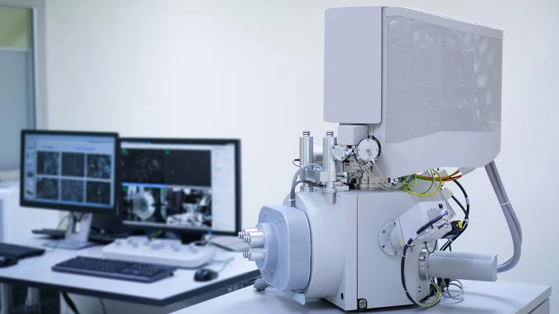
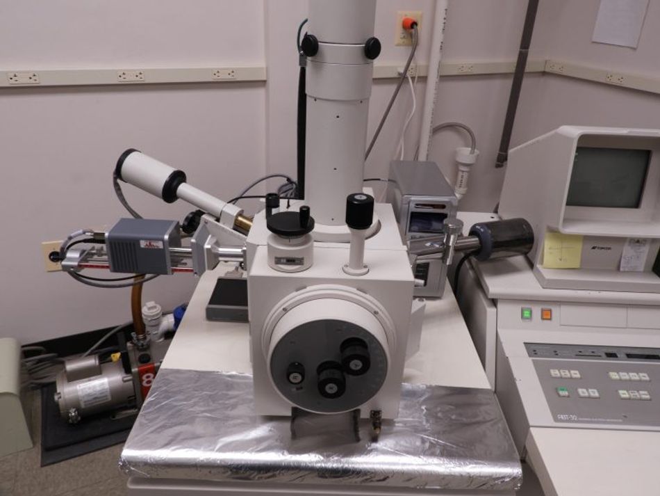
Scanning Electron Microscope (SEM) Machine in Laboratory
Introduction
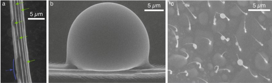
Scanning electron microscopy (SEM) is a powerful imaging technique that has revolutionized the way we visualize and analyze materials at the micro and nano scales. With applications spanning across diverse fields such as materials science, biology, and geology, SEM has become an indispensable tool for researchers and industry professionals alike. Scanning Electron Microscopy offers high-resolution images, providing insights into the structure, composition, and properties of various samples. These traits make SEM a useful technique for various applications, including biology, engineering, and forensics.
Basics of Scanning Electron Microscopy
Scanning electron microscopy (SEM) relies on the interaction between a focused electron beam and a sample to generate high-resolution images. One of the key advantages of SEM over other microscopy techniques is its ability to achieve much higher resolution, typically in the range of 1-10 nanometers. Some SEMs can achieve resolutions better than 1 nanometer. [1] This allows researchers to study the fine details of a sample's surface topography, composition, and other properties.
Electron Beam Generation and Interaction with Samples
In SEM, cathode is the source of the electron beam. The electron beam is generated by an electron source, typically a tungsten filament or an electron gun. The electron source emits electrons through a process called thermionic emission or field emission, depending on the type of source. The emitted electrons are then accelerated by an electric field and focused into a narrow beam using a series of electromagnetic lenses. The driving charges are termed as accelerating voltage. The electrons are accelerated through a vacuum column to high energy, typically between 1 and 30 kV. [2] The electron beam is scanned across the surface of the sample in a raster pattern, allowing for the collection of information from each point on the sample.
When the electron beam interacts with the sample, various signals are produced, which include secondary electrons, backscattered electrons, and characteristic X-rays.
Secondary electrons are emitted from the sample surface due to the inelastic scattering of the incident electrons. These low-energy electrons provide information about the sample's surface topography and morphology.
Backscattered electrons, on the other hand, are high-energy electrons that have been elastically scattered by the sample's atomic nuclei. They provide information about the sample's composition and can be used to generate elemental maps.
Characteristic X-rays are emitted when the incident electrons displace inner-shell electrons in the sample's atoms, causing outer-shell electrons to fill the vacancies and release energy in the form of X-rays. These can be used for elemental analysis and quantification.
The various signals produced during the interaction between the electron beam and the sample are detected and processed to form images or elemental maps. These provide valuable information about the sample's structure, composition, and properties.
Electron Detectors and Image Formation
Electron detectors play a crucial role in SEM by capturing the signals generated during the interaction between the electron beam and the sample. There are several types of electron detectors used, each with its unique characteristics and applications.
Everhart-Thornley Detector (ETD) is the most common detector used for capturing secondary electrons (SE). It consists of a scintillator that converts the incident SE into photons, which are then multiplied by a photomultiplier tube to produce an electrical signal. The ETD is typically positioned at an angle to the sample, allowing it to efficiently collect SE emitted from the sample surface. The high sensitivity of ETDs enables them to produce high-resolution images with excellent surface detail. [3]
Backscattered Electron Detectors (BSED) are designed to capture backscattered electrons (BSE) that are reflected from the sample surface. BSEDs are usually positioned above the sample, directly opposite the electron beam. BSE images provide information about the sample's composition. The intensity of backscattered electrons is directly related to the atomic number of elements in the sample. This makes BSEDs particularly useful for studying materials with varying compositions.
Energy-Dispersive X-ray Detectors (EDX) are used to detect characteristic X-rays emitted from the sample during the interaction with the electron beam. These rays provide elemental information about the sample, allowing for quantitative and qualitative analysis of its composition. EDX detectors typically use a silicon drift detector (SDD) or a lithium-drifted silicon (Si(Li)) detector to capture the X-rays and convert them into electrical signals. The energy is then analyzed to determine the elements present in the sample and their relative concentrations.
The detected signals from these detectors are processed and used to form images that reveal various aspects of the sample. In SEM, the image formation process involves scanning the electron beam across the sample surface in a raster pattern. This information is then used to generate a two-dimensional image, where each pixel corresponds to a specific location on the sample surface, and its intensity represents the signal strength at that point. By combining the images obtained from different detectors, it is possible to obtain a comprehensive understanding of the sample's structure, composition, and properties.
Sample Preparation for SEM
Proper sample preparation is crucial for obtaining accurate and meaningful results in scanning electron microscopy. The preparation process varies depending on the type of sample being analyzed and the specific imaging or analytical technique being used. In general, sample preparation for SEM involves several steps, such as cleaning, mounting, and coating the sample and adjusting the sample's size and shape to fit within the microscope's chamber.

Conductive Coating
One important aspect of sample preparation for SEM is the application of a conductive coating to non-conductive samples. This is necessary because the electron beam used in SEM can cause charging effects on the surface of non-conductive samples, leading to image distortion and other artifacts. Applying a thin layer of conductive material, such as gold, platinum, or carbon, minimizes the charging effects, resulting in clearer and more accurate images.
There are several methods for applying coatings to samples, including sputter coating and evaporative coating. In sputter coating, a target material (e.g., gold or platinum) is bombarded with ions, causing atoms from the target to be ejected and deposited onto the sample surface. This method produces a uniform and thin conductive layer, typically in the range of a few nanometers in thickness. Evaporative coating involves heating the coating material in a vacuum chamber until it evaporates and condenses onto the sample surface. This method can also produce a uniform conductive layer, but it may be less suitable for samples that are sensitive to heat. [4]
Each type of coating has its advantages and disadvantages. For example, gold and platinum coatings provide excellent conductivity and are compatible with a wide range of samples, but they can be expensive and may introduce artifacts in some cases. Carbon coatings are less expensive and less likely to cause artifacts, but they may not provide sufficient conductivity for all applications. The choice of coating material and method depends on the specific requirements of the analysis and the properties of the sample being studied.
Cryo-SEM
Cryo-scanning electron microscopy (cryo-SEM) is a specialized technique designed for imaging hydrated and biological samples that are sensitive to the high vacuum environment and electron beam exposure in conventional SEM. Cryo-SEM allows for the preservation of the native state of these samples by rapidly freezing them. This is done while maintaining their structure and preventing dehydration or other artifacts that may occur during sample preparation.
Cryo-fixation process involves rapidly freezing the sample, typically by plunging it into a cryogenic liquid such as liquid nitrogen or liquid ethane. This rapid freezing minimizes the formation of ice crystals, which can damage the sample's structure. Once the sample is cryo-fixed, it is transferred to the cryo-stage within SEM, maintained at cryogenic temperatures throughout the imaging process.
Cryo-fracture is another technique employed in cryo-SEM to expose the internal structures of the sample. The frozen sample is fractured, either mechanically or by using a focused ion beam, revealing the interior structures that can then be imaged using SEM. This method is particularly useful for studying the internal organization of cells, tissues, and other biological samples. [5]
Cryo-SEM offers several advantages over conventional SEM for imaging sensitive samples. By preserving the sample in its native, hydrated state, cryo-SEM provides more accurate and representative images of the sample's structure and composition. Additionally, cryo-SEM can be used to study dynamic processes, such as the freezing and thawing of materials, by capturing snapshots of these processes at different stages. However, cryo-SEM also has some limitations, including the need for specialized equipment and expertise, and the potential for sample damage during cryo-fixation or cryo-fracture. Despite these challenges, cryo-SEM remains a valuable tool for studying a wide range of sensitive samples and processes.
Recommended reading: Cryo-imaging lifts the lid on fuel cell catalyst layers
SEM Imaging Modes and Techniques
Scanning electron microscopy offers a variety of imaging modes and techniques that can be used to obtain different types of information about a sample. These modes and techniques are based on the detection and analysis of various signals generated during the interaction between the electron beam and the sample. By selecting the appropriate imaging mode or technique, researchers can tailor the SEM analysis to their specific needs and obtain valuable insights.
Secondary Electron Imaging
Secondary electron imaging is one of the most commonly used imaging modes in SEM. It relies on the detection of secondary electrons, which are low-energy electrons emitted from the sample surface as a result of the inelastic scattering of the incident electron beam. These images provide detailed information about the sample's surface topography and morphology. This is because the intensity of the detected secondary electrons is highly sensitive to the surface features and the angle of incidence of the electron beam.
In secondary electron imaging, the sample is scanned with the electron beam, and the emitted secondary electrons are collected by a detector, such as an Everhart-Thornley detector. The intensity of the detected secondary electrons is used to generate a two-dimensional image. Each pixel corresponds to a specific location on the sample surface, and its intensity represents the number of secondary electrons emitted from that point. The wavelength of the electron beam in an SEM is related to the resolution of the SEM. The shorter the wavelength, the higher the resolution. This results in high-resolution images that reveal the fine details of the sample's surface, such as grain boundaries, defects, and other features.
Secondary electron imaging is particularly useful for studying the surface morphology of materials and analyzing the distribution of particles, fibers, or other features on the sample surface. Additionally, secondary electron images can be combined with other imaging modes or analytical techniques to obtain a more comprehensive understanding of the sample's structure and composition.
Backscattered Electron Imaging
Backscattered electron imaging is another important imaging mode in scanning electron microscopy. It relies on the detection of backscattered electrons (BSE) that are elastically scattered by the sample's atomic nuclei. Unlike secondary electrons, backscattered electrons carry information about the sample's composition and can be used to generate elemental maps. [6]
The intensity of backscattered electrons is directly related to the atomic number (Z) of the elements present in the sample. When the incident electron beam interacts with the sample, high-Z elements scatter more electrons back towards the detector than low-Z elements. This results in a contrast in the BSE image, with high-Z regions appearing brighter and low-Z regions appearing darker. This contrast allows for the identification of different phases, inclusions, or compositional variations within the sample.
Backscattered electron imaging offers several advantages over secondary electron imaging. First, BSE images provide compositional information, making them particularly useful for studying materials with varying compositions or identifying phases and inclusions within a sample. Second, BSE images have a greater depth of field than SE images, allowing for the visualization of sample features at different depths without the need for refocusing. This can be especially useful for studying rough or uneven surfaces.
However, backscattered electron imaging also has some limitations. The resolution of BSE images is generally lower than that of SE images, as the backscattered electrons originate from a larger interaction volume within the sample. Additionally, BSE images can be more susceptible to charging artifacts in non-conductive samples, as the high-energy backscattered electrons can cause localized charging on the sample surface.
Despite these limitations, backscattered electron imaging remains a valuable tool in SEM for studying the composition and structure of a wide range of materials. This provides complementary information to secondary electron imaging and other analytical techniques.
Energy-Dispersive X-ray Spectroscopy
Energy-dispersive X-ray spectroscopy (EDS) is an analytical technique used in conjunction with SEM to obtain elemental information about a sample. EDS is based on the detection and analysis of characteristic X-rays emitted from the sample during the interaction with the electron beam. These X-rays provide valuable insights into the elemental composition and distribution within the sample.
When the incident electrons in the SEM displace inner-shell electrons in the sample's atoms, outer-shell electrons, fill the vacancies, releasing energy in the form of characteristic X-rays. The energy of these X-rays is unique to each element, allowing for the identification of the elements present in the sample. EDS detectors, such as silicon drift detectors (SDD) or lithium-drifted silicon (Si(Li)) detectors, capture the emitted X-rays and convert them into electrical signals. The energy of the X-rays is then analyzed to determine the elements present in the sample and their relative concentrations.
EDS has several advantages as an analytical technique in SEM. It is non-destructive, allowing for the analysis of samples without causing damage or altering their properties. EDS can also detect elements with atomic numbers as low as boron (Z=5), making it suitable for analyzing a wide range of materials. Furthermore, EDS can be used for both qualitative and quantitative analysis, providing information on the presence of elements as well as their relative concentrations. [7]
In addition to elemental mapping, EDS can also be used for other applications. These include identification of phases in materials, the study of chemical reactions and processes, and the analysis of thin films and coatings. By combining EDS with other SEM imaging techniquesresearchers can obtain a comprehensive understanding of the sample's structure, composition, and properties.
Recommended reading: Atomic Force Microscopy Explained: Principles, Construction, Working, and Applications
Advanced SEM Techniques
In addition to the conventional imaging modes and techniques, several advanced SEM techniques have been developed to extend the capabilities of the light microscope and address specific requirements in sample analysis.
Environmental SEM
In ESEM, the sample is placed in a specially designed sample chamber that can be maintained at a specific pressure and humidity level. The electron beam is then transmitted through a series of differential pumping apertures. This separates the high vacuum region of the electron column from the lower vacuum region of the sample chamber. This allows the electron beam to interact with the sample without the need for a high vacuum environment.
The advantages of ESEM include the ability to study samples in their natural, hydrated state and the possibility of observing dynamic processes, such as wetting, drying, or phase transitions, in real-time. ESEM can also be used to study samples that are sensitive to electron beam damage. The presence of water vapor in the sample chamber can help mitigate the electron beam's effects on the sample.
ESEM has found applications in various fields, including materials science, biology, and geology, where it has been used to study phenomena such as corrosion, hydration, and the behavior of water in porous materials. Despite its advantages, this technique has some limitations, such as reduced spatial resolution compared to conventional SEM. Another one is the need for specialized equipment and expertise to operate the microscope under controlled environmental conditions.
Focused Ion Beam-SEM
Focused ion beam-scanning electron microscopy (FIB-SEM) is a powerful technique that combines the capabilities of a focused ion beam (FIB) system with those of an SEM, enabling the simultaneous milling and imaging of samples at high resolution. FIB-SEM is particularly useful for the preparation of site-specific cross-sections, the fabrication of nanostructures, and the three-dimensional reconstruction of samples.
Magnification in an SEM is controlled over a range of about 6 orders of magnitude from about 10 to 3,000,000 times. Unlike optical and transmission electron microscopes, image magnification in an SEM is not a function of the power of the objective lens.
In FIB-SEM, a focused beam of ions, typically gallium ions, is used to sputter away material from the sample surface This allows the precise removal of material and the creation of cross-sections or other structures. The ion beam can be controlled with nanometer precision, enabling the fabrication of intricate features or the selective removal of specific regions of the sample. Source ions are then generally accelerated to an energy of 1–50 kilo electronvolts (0.16–8.01 fJ), and focused onto the sample by electrostatic lenses. [8] Simultaneously, the SEM is used to image the sample, providing high-resolution information about the sample's structure and composition.
One of the key applications of FIB-SEM is the preparation of site-specific cross-sections for materials analysis. By using the FIB to mill away material, researchers can expose the internal structure of the sample and then image it using the SEM. This allows for the study of buried interfaces, grain boundaries, and other features that are not accessible using conventional SEM techniques.
FIB-SEM is also widely used for the three-dimensional reconstruction of samples, particularly in the field of biological imaging. By sequentially milling away thin layers of the sample and imaging each layer using the SEM, researchers can obtain a series of two-dimensional images that can be combined to create a three-dimensional representation of the sample. This technique, known as serial block-face imaging or FIB-SEM tomography, has been used to study the ultrastructure of cells, tissues, and other biological samples at nanometer resolution.
Despite its many advantages, FIB-SEM also has some limitations. This includes the potential for sample damage due to ion beam irradiation and the relatively slow milling and imaging process compared to other techniques. However, the unique capabilities of FIB-SEM make it an invaluable tool for a wide range of applications in materials science, biology, and other fields.
Applications of SEM in Various Fields
Scanning electron microscopy has a wide range of applications across diverse fields. By combining SEM imaging techniques and analytical capabilities, SEM has contributed to advancements in materials science, biology, geology, and many other areas of research and technology.
Materials Science
In materials science, SEM plays a crucial role in the study of microstructures, defects, and other features that influence the properties and performance of materials. High-resolution SEM images provide detailed information about the spot size, shape, and distribution of grains, phases, and other microstructural features. This allows researchers to understand the relationships between microstructure and material properties.
For example, SEM can be used to study the grain boundaries in metals and alloys, which can significantly impact mechanical properties, such as strength and ductility. By analyzing the grain boundary structure and chemistry using SEM imaging and EDS, researchers can develop strategies to optimize the processing and performance of these materials. [9]
SEM is also widely used in the analysis of thin films and coatings, which are critical components in many advanced technologies, such as microelectronics, solar cells, and protective coatings. SEM can provide information on the thickness, morphology, composition of these films, and physical properties of semiconductors. However, it is not a diffraction instrument.
In addition to these applications, SEM has been used to study a wide range of materials, including ceramics, polymers, composites, and biomaterials. This contributes to the development of new materials and technologies in various fields. SEM has become an indispensable tool in materials science research and development by providing detailed information on the structure and composition of these materials.
Biology and Life Sciences
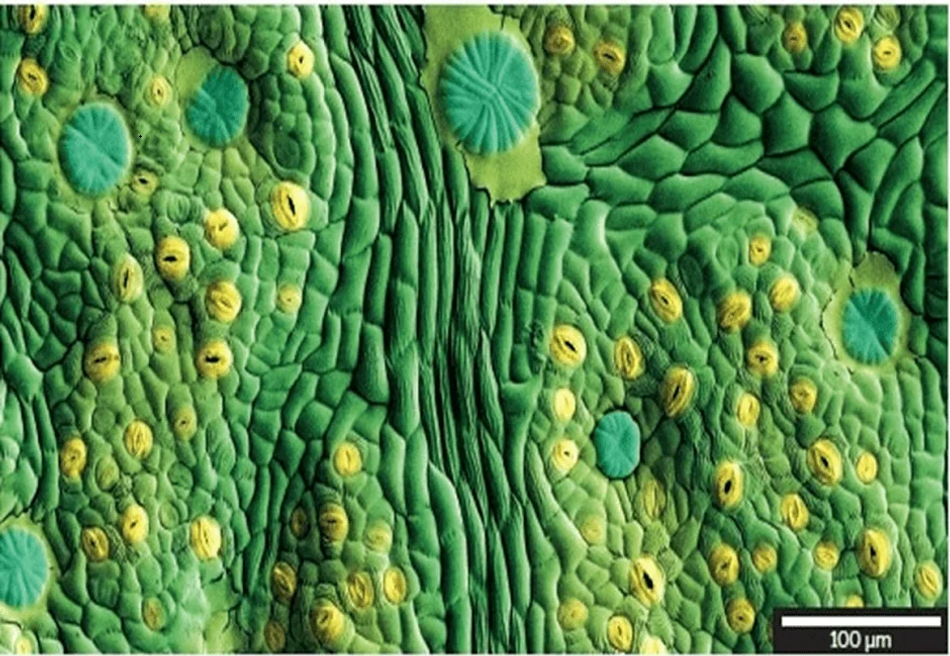
Scanning electron microscopy has made significant contributions to the field of biology and life sciences. This enables researchers to study the intricate details of cellular structures, tissues, and biological materials at high resolution. The versatility of SEM, has led to numerous discoveries and advancements in our understanding of biological processes and systems.
One of the key applications of SEM in biology is the imaging of cellular structures, such as cell membranes, organelles, and extracellular matrices. By providing high-resolution images of these structures, SEM has helped researchers elucidate their function and organization and investigate the interactions between cells and their environment. For example, SEM has been used to study the morphology of bacterial cells, the organization of cytoskeletal elements, and the structure of extracellular matrix components, such as collagen and elastin.
In addition to cellular structures, SEM has also been used to study the morphology and organization of tissues, both in healthy and diseased states. This has led to a better understanding of tissue architecture and the role of specific cell types in the maintenance and function of tissues. For instance, SEM has been employed to investigate the structure of blood vessels, the organization of connective tissues, and the changes that occur in tissues during disease progression.
Advanced SEM techniques have expanded the range of biological samples that can be studied using electron microscopy. Cryo-SEM, in particular, has been instrumental in the imaging of hydrated and biological samples. This allows researchers to study the native state of cells, tissues, and biomolecules without the need for dehydration or other sample preparation steps that may introduce artifacts.
Overall, scanning electron microscopy has played a crucial role in advancing our understanding of biological processes and systems. As new SEM techniques and technologies continue to be developed, the potential for further discoveries and insights in the field of biology and life sciences remains vast.
Geology and Earth Sciences
Scanning electron light microscopy has become valuable tool in the field of geology and earth sciences. The high-resolution imaging capabilities of SEM have contributed significantly to our understanding of Earth's history, processes, and the formation of its various geological features.
Mineralogy and Petrology: SEM is widely used in the study of minerals and rocks, allowing for the detailed examination of their crystal structures, grain boundaries, and chemical compositions. By analyzing the distribution of elements within a sample, researchers can gain insights into the processes that led to the formation of the minerals and rocks and their subsequent alteration and metamorphism. Additionally, SEM can be used to study the microstructure of rocks, revealing information about their deformation history and mechanical properties.
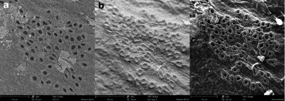
Sedimentology and Paleontology: The high-resolution imaging capabilities of SEM make it an ideal tool for studying the morphology and microstructure of sedimentary particles and fossils. [10] By examining the shape, spot size, and surface features of these particles, researchers can infer information about their transport history, depositional environment, and diagenetic processes. In paleontology, SEM can be used to study the fine details of fossilized organisms, providing insights into their biology, ecology, and evolution.
Environmental Geology and Geochemistry: SEM is also used to study the interactions between geological materials and environmental processes, such as weathering, erosion, and pollution. By analyzing the chemical composition and microstructure of samples exposed to different environmental conditions. This way, researchers can gain insights into the mechanisms of these processes and their impact on the geological materials. This information is crucial for understanding the long-term stability of geological structures and assessing the environmental impact of human activities on the Earth's surface.
In summary, scanning electron microscopy has become an indispensable tool in the field of geology and earth sciences, providing researchers with the ability to study a wide range of geological samples at the micro and nano scales. The high-resolution imaging and analytical capabilities of SEM have contributed significantly, paving the way for new discoveries and advancements in the field.
Conclusion
Scanning electron microscopy has revolutionized the study of materials, biological samples, geological specimens, and many other fields by providing high-resolution imaging and analytical capabilities. The versatility of SEM, combined with advanced techniques such as cryo-SEM, ESEM, and FIB-SEM. This has enabled researchers to explore a wide range of samples and obtain valuable insights into their structure, composition, and properties. As new SEM techniques and technologies continue to be developed, the potential for further discoveries and advancements across various disciplines remains vast.
Frequently Asked Questions
1. What is the difference between SEM and transmission electron microscopy (TEM)?
A. SEM and TEM are both electron microscopy techniques, but they differ in their operating principles and the type of information they provide. SEM scans the sample surface with an electron beam and detects secondary or backscattered electrons to generate high-resolution images of the sample's surface topography and composition. TEM, on the other hand, transmits an electron beam through a thin sample and forms an image based on the transmitted beam of electrons. This provides user information about the internal structure of the sample at even higher resolution than SEM.
2. Can SEM be used to study non-conductive samples?
A. Yes, SEM can be used to study non-conductive samples, but special sample preparation techniques or imaging conditions may be required to minimize charging artifacts. Common approaches include coating the sample with a thin conductive layer, such as gold or carbon, or using low-voltage SEM or environmental SEM to reduce charging effects.
3. What is the typical resolution of SEM?
A. The resolution of SEM depends on various factors, such as the electron beam energy, the type of detector used, and the sample properties. SEM image of a metal surface might show features that are a few microns in size. In general, modern SEMs can achieve resolutions in the range of 1-2 nanometers for secondary electron imaging and slightly lower resolutions for backscattered electron imaging.
4. How do I prepare a sample for SEM analysis?
A. Sample preparation for SEM depends on the type of sample and the information required from the analysis. Common preparation steps include mounting the sample on a suitable holder, drying or dehydrating the sample, and coating it with a conductive material if necessary. For biological samples, more specialized preparation techniques, such as fixation, dehydration, and critical point drying, may be required to preserve the sample's structure.
5. Can SEM be used for elemental analysis?
A. Yes, SEM can be used for elemental analysis by combining it with energy-dispersive X-ray spectroscopy. EDS detects the characteristic X-rays emitted from the sample during the interaction with the electron beam, providing information about the elemental composition and distribution within the sample.
6. What SEM techniques can be used in a low vacuum environment?
A. Low-vacuum scanning electron microscopy (LVSEM) is a technique that is used to image samples that cannot be placed in a high vacuum, such as biological samples or samples that contain water. It allows for the study of the elemental composition, and physical properties of a wide variety of samples.
References
1. Wikipedia. Scanning Electron Microscope. [Cited 2023 August 01] Available at: Link
2. Uiowa. Scanning Electron Microscopy. [Cited 2023 August 01] Available at: Link
3. IOPscience. Wide-band detector for micro-microampere low-energy electron currents. [Cited 2023 August 01] Available at: Link
4. Leica-microsystems. Brief Introduction to Coating Technology for Electron Microscopy. [Cited 2023 August 01] Available at: Link
5. Cambridge. Cryo-Fracture or Freeze-Fracture, a Method to Expose Internal Tissue Surfaces and Cell Surfaces for Viewing in the Scanning Electron Microscope. [Cited 2023 August 01] Available at: Link
6. Thermofisher. Backscattered Electrons in SEM Imaging. [Cited 2023 August 01] Available at: Link
7. Rtilab. SEM/EDS Analysis. [Cited 2023 August 01] Available at: Link
8. Wikipedia. Focused Ion Beam. [Cited 2023 August 01] Available at: Link
9. Sciencedirect. Scanning electron microscopy for materials characterization. [Cited 2023 August 01] Available at: Link
10. Sciencedirect. Scanning Electron Microscopy in Palaeontological Studies. [Cited 2023 August 01] Available at: Link