Building devices at the atomic scale: the spatial revolution
Researchers and companies unite to advance an established fabrication technique that builds up materials atom by atom for use in displays, batteries, and solar panels.

11 Feb, 2021. 4 minutes read
You’re most likely reading this article on a device containing microchips, which in turn contain millions of transistors. The placement of these nanometer-sized components in microchips is only possible with accurate fabrication techniques like atomic layer deposition (ALD). But to use this atom-by-atom build-up technique to make larger scale devices such as displays and solar cells, ALD needs an upgrade; a spatial one, to be precise. TU/e researchers Bart Macco and Erwin Kessels, in collaboration with numerous companies, aim to elevate this ‘spatial ALD’ to the next level. Get ready for the spatial revolution.
Independent developments are regular in science. Just think of Elisha Gray and Alexander Graham Bell with the telephone, or Isaac Newton and Gottfried Wilhelm Leibniz with calculus.
Like the telephone and calculus, atomic layer deposition was also developed by independent groups, in this case, Russian and Finnish scientists in the 1960s and 1970s respectively.
The magic of atomic layer deposition is all in the name – it puts layers of atoms on top of layers of atoms. “ALD allows for the growth of layers of atoms in a controlled manner – which is hugely important for electronic products like processors and memory devices,” says TU/e researcher Bart Macco.
How To Build An Atomic Sandwich
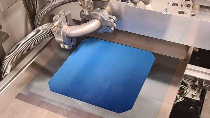
ALD takes place in a chamber under vacuum conditions with the atoms deposited on a starting layer or substrate. This substrate is exposed to chemical reactants in a gas, and some reactants attach to the substrate. Unused reactants and by-products are then removed before the next chemical reactant is introduced and deposited on top of the layer below. “It’s like building an atomic sandwich,” notes Macco.
TU/e has been working on ALD for some time, as Erwin Kessels fondly remembers. “Back in 2003, when I was a young assistant professor in the Plasma & Materials Processing (PMP) group, I was working on a project with 2 PhD students on ALD. Nowadays, the group focus is very much on ALD.”
Video showing the difference between temporal and spatial ALD. Source: AtomicLimits (YouTube).
Shifting From Temporal To Spatial
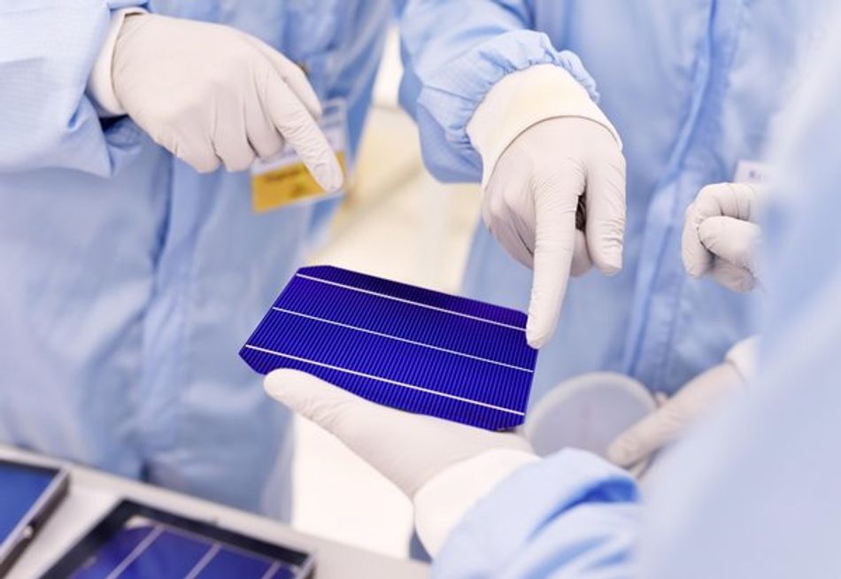
Given that layers are deposited one after another on a stationary substrate over time, ALD can also be referred to as temporal ALD. While temporal ALD has the accuracy needed to make microchips and has already proven itself in high-volume solar cell production, it’s not well suited for high-volume production of other devices with large surface areas like displays. “There’s a speed issue, and in industry if the technique is too slow then it’s not useful,” says Kessels.
Nonetheless, there is an ALD approach that provides the necessary scale-up and high-volume production speeds needed for industry. And it involves thinking spatially.
Flying Substrates Save The Day
“In spatial ALD, layers are grown much faster by “flying” the substrate through different zones of the reactor with each zone containing different gases or reactants,” says Macco.
“Flying” the substrate allows for the faster deposition of layers, while retaining accuracy. It’s very much a case of flying faster is better.
Although spatial ALD was patented in the early 1980s, it wasn’t until the second half of the 2000s that spatial ALD started gaining scientific attention. This means that there’s still a lot unknown about spatial ALD.
Added to that, innovating spatial ALD is not going to be easy. Bart Macco: “Our slogan is ‘More materials, more demanding applications’. We want to use spatial ALD to deposit a wider range of complex materials for new applications. This might involve building layers on flexible or porous substrates. There are lots of things to solve, but it’s a thrilling challenge.”
Assembling The Spatial Ald Team
Many Dutch companies are working on spatial ALD equipment such as Levitech, SoLayTec, SALD, Smit Thermal Solutions, VDL-ETG, TNO, and SALDtech. Thanks to a grant of 700,000 euros from the Dutch Research Council’s (NWO) Open Technology Programme, Macco and Kessels aim to improve the competitive edge of Dutch spatial ALD companies by working directly with these companies, and establishing a hub of spatial ALD innovation at TU/e.
In addition to stakeholders like ASM, Chipmetrics, and J.A. Woollam, these companies, some of whom are working on sustainable energy technologies, will be heavily involved in the NWO-funded project. “The Netherlands is playing a leading role in the field of spatial ALD, and we want TU/e to be the principle contributor to advancements,” says Macco, who is also the project coordinator.
“This project will assemble many companies to work on spatial ALD technology, but they all have their own different applications,” adds Macco. “Exciting times lie ahead for spatial ALD at TU/e.”
Welcoming New Equipment
And the most exciting aspect of the project will be the in-kind installation of a spatial ALD tool – developed by the company SALD – in the laboratories of the PMP group at TU/e. The tool is a dedicated R & D system that can be easily reconfigured to study the influence of various factors on the spatial ALD process.
Erwin Kessels: “Having access to this tool will be invaluable to the success of the project. We can test new processes, new materials, and new substrates quickly. It promises to be fun!”
It goes without saying that Kessels and Macco are enthusiastic about upcoming developments in spatial ALD. What’s more, they and their collaborators in academia and industry are set to play leading roles in the ongoing narrative of spatial ALD.
Move over temporal ALD, and make some space for spatial ALD at the fabrication table.