What are Gerber Files? Understanding the Blueprint of Electronics Manufacturing
This article provides an in-depth view of Gerber files, including their origin, structure, and role in PCB design and manufacturing processes.

20 Nov, 2023. 13 minutes read
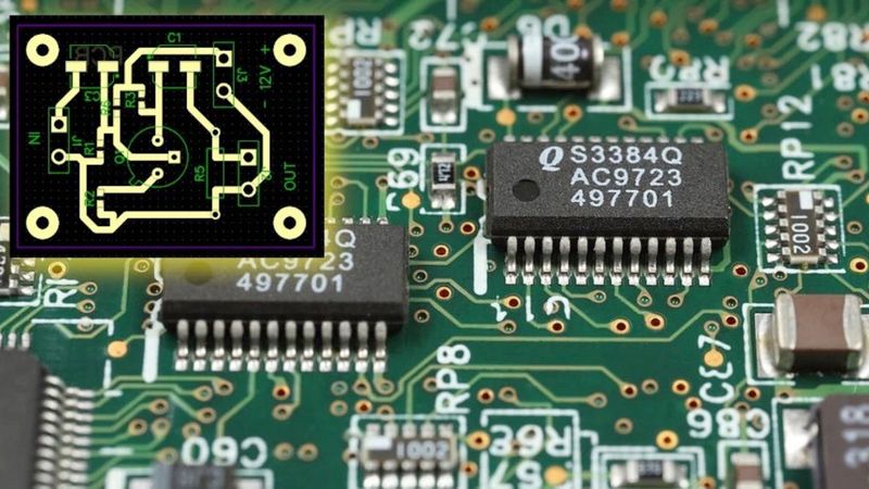
Gerber File Schematic in PCB Manufacturing
What are Gerber Files?
Gerber files are essential in the electronics manufacturing industry. These files are essentially the blueprint that guides the production of printed circuit boards (PCBs), found virtually in all electronic devices. The Gerber file format is the de facto standard PCB industry software used to describe the images of printed circuit boards, including copper layers, solder masks, and legends.
Gerber files are a universal language for electronics manufacturing, bridging digital design and physical production. They are the essential link that allows the complex designs of electronic engineers to be accurately and reliably brought to life. Files with .gbr extension is a Gerber image file format for exchange of printed circuit board (PCB) design data transfer. What are Gerber files in practical terms?
Let’s understand it using an example. Consider a complex piece of equipment like a smartphone. It contains a PCB that hosts the device's processor, memory, and other critical components. The design of this PCB, with its numerous layers and precise pathways for electrical currents, is communicated to the manufacturing equipment through a Gerber file. Without this file, accurately producing the PCB to the necessary specifications would be virtually impossible.
Curious about what are Gerber files? Let’s delve into their origin, structure, manufacturing process, and the role of Gerber Files in PCB design.
The Origin of Gerber Files
The Gerber file format was created in the 1960s by Gerber Systems Corp., a company that was a pioneer in photoplotting, a process used to create printed circuit boards. They developed the Gerber format to control their photoplotters, machines that created high-quality, large-format photographic images of PCB designs. The format was initially exclusive to Gerber Systems Corp., but the demand for a standard file format for PCB design increased with the evolution of the electronics industry.
The first Gerber files were very simple. They consisted of a series of commands that told the printer where to draw lines and circles on the PCB. These early Gerber files were not very versatile, but they were enough to complete the job. In the 1980s, Gerber Systems developed an extended Gerber format that was more versatile than the original format. The extended Gerber format introduced new commands for drawing complex shapes, such as arcs and curves. It also introduced the concept of apertures, which are templates that can be used to draw shapes with different properties.
Over the years, the Gerber format has evolved to keep pace with the increasing complexity of PCB designs. The current version, Extended Gerber or RS-274X, includes several enhancements over the original format. [1] There are now Gerber files for a variety of PCB manufacturing processes, such as photoresist etching, screen printing, and solder paste deposition.
Despite the emergence of other file formats, the Gerber format remains the most widely used in the electronics manufacturing industry. Its longevity can be attributed to its robustness, flexibility, and the fact that it is an open standard. This has allowed it to maintain its position as the go-to format for PCB design, even as the electronics industry continues to evolve and grow.
Recommended Reading: PCBA Design-Five Tips to Clean Up Your Layout
Understanding the Structure of Gerber Files
A Gerber file is a 2D binary vector image that describes one layer of a printed circuit board. It is composed of a series of commands that define the shapes and positions of the various elements on the PCB layer. These commands are written in a language the photoplotting machines used in PCB manufacturing understand.
The structure of a Gerber file is relatively simple. It consists of a header, a series of data blocks, and an end-of-file marker. The header contains information about the file format and the units of measurement used in the file. The data blocks contain the commands that describe the PCB layer. Each command is a text line specifying a particular operation, such as drawing a line or flashing a pad.
The commands in a .gbr file are grouped into two categories: draw and flash. Draw commands are used to create lines and arcs, while flash commands are used to create pads and other filled shapes. Each command specifies the shape, size, and position of the element it creates.
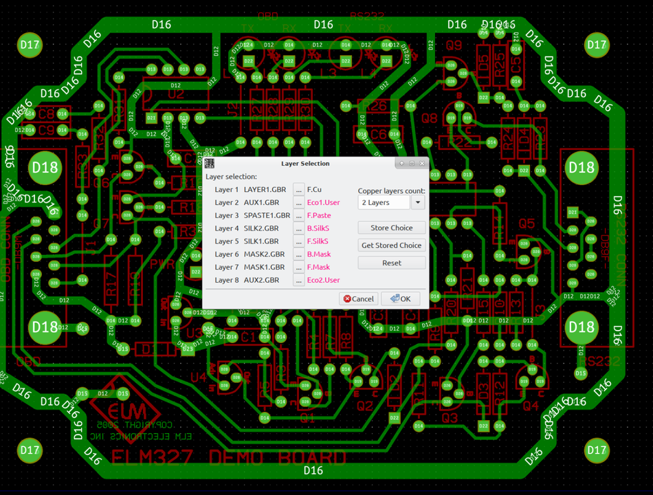
Layers in Gerber Files
Gerber files are composed of multiple layers, each representing a specific feature of the printed circuit board (PCB). For example, the copper layers carry the electrical signals, the solder mask layers prevent solder bridges, and the silkscreen layers provide a reference for assembly and troubleshooting. [2]
Each layer in a Gerber file is described independently of the others. This means that the photoplotting machine can process each layer separately, allowing for high precision and control in the manufacturing process. The machine uses the information in the Gerber file to accurately reproduce the design on the corresponding layer of the PCB.
For example, a simple two-layer PCB would have separate Gerber files for the top copper, bottom copper, top solder mask, bottom solder mask, top silkscreen, and bottom layer silkscreen. Each separate file would contain the commands necessary to create the elements on that layer. The photoplotting machine would then use these files to create the PCB, layer by layer.
In addition to the standard set of Gerber layers, there are also a number of non-standard Gerber layers that can be used for specific applications. For example, there are Gerber layers for creating solder paste stencils, defining copper pours, and defining keep-out zones.
The specific Gerber layers that are required for a given PCB design will depend on the complexity of the design. For simple designs, only a few Gerber layers may be required. For more complex designs, a large number of Gerber layers may be required.
Data Formats in Gerber Files
Gerber files utilize specific data formats to represent the various elements of a PCB design. These formats are essential for ensuring that the information in the file extension can be accurately interpreted by the photoplotting machines used in PCB manufacturing. Two primary data formats are used in Gerber files: RS-274-D and RS-274X. [3]
RS-274-D, also known as the Standard Gerber format, is the older of the two formats. It is a simple, human-readable ASCII format that uses a series of commands to describe the shapes and positions of the elements on a PCB layer. Each command is a text line specifying a particular operation, such as drawing a line or flashing a pad. The RS-274-D format has some limitations, such as the lack of support for complex shapes and the need for a separate aperture file to define the sizes and shapes of the pads and traces.
RS-274X, or Extended Gerber, is an enhanced version of the Standard Gerber format. It was developed to address the limitations of the older format and to provide additional functionality. The RS-274X format includes several improvements over the RS-274-D format, such as:
Embedded aperture definitions: In RS-274X, aperture definitions are included directly in the Gerber file, eliminating the need for a separate aperture file. This simplifies the text file management process and reduces the risk of errors.
Support for complex shapes: The RS-274X format defines complex shapes, such as polygons and curved lines. This enables designers to create more intricate PCB designs and allows for greater flexibility in the manufacturing process.
Inclusion of metadata: RS-274X files can include metadata, such as layer names, units of measurement, and other information that can be useful for designers and manufacturers.
Support for multiple layers: The RS-274X format supports the definition of multiple layers within a single file, making it easier to manage and process complex, multi-layer PCB designs.
Due to its enhanced capabilities and widespread adoption, the RS-274X format has become the de facto standard for PCB Gerber files in electronics manufacturing. Its ability to accurately represent complex PCB designs and its compatibility with modern manufacturing equipment make it the preferred choice for PCB designers and manufacturers.
Recommended Reading: How to Design a PCB Layout: A Comprehensive Guide
The Role of Gerber Files in PCB Design
Gerber files play a crucial role in printed circuit board (PCB) design and manufacturing. They serve as the bridge between the digital design created by engineers and the physical board produced by manufacturing equipment.
In the design phase, engineers use specialized software to create a digital representation of the PCB. This includes the layout of the board, the placement of components, and the routing of electrical connections. The software then translates this design into a series of Gerber files, each representing a different layer or aspect of the PCB.
The Gerber files provide a detailed map for the manufacturing equipment, guiding the creation of each layer of the PCB. They specify the shapes, sizes, cutouts, and positions of all the elements on the board, from the smallest trace to the largest component. This ensures that the physical board accurately reflects the original board design.
Translating Design to Manufacturing
The translation of a PCB design into a set of Gerber files is a critical step in the manufacturing process. It involves converting the complex, multi-layered design into a format that can be understood by the photoplotting machines used in PCB production.
This process begins with the design software, which breaks the PCB design into its constituent layers. Each layer is then converted into a separate Gerber file. The software generates a series of commands for each file, describing the shapes and positions of the elements on that layer.
The Gerber files are then sent to the PCB manufacturer, loaded into the photoplotting machines. These machines use the information in the Gerber files to create each layer of the PCB. They follow the commands in the files to draw the traces, flash the pads, and perform other operations necessary to create the board.
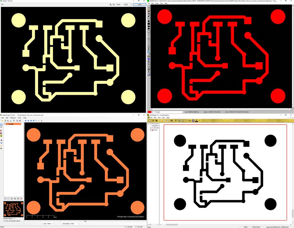
The accuracy of the Gerber files is crucial to the success of the manufacturing process. Any errors or inaccuracies in the files can result in defects in the final product. Therefore, PCB designers often use Gerber viewers, software tools that allow them to preview the Gerber files and check for errors before sending them to the manufacturer. [4]
In essence, Gerber files serve as the blueprint for PCB fabrication. They translate the intricate designs of engineers into a language that the manufacturing equipment can understand, ensuring that the final product accurately reflects the original design.
Checking and Verifying Designs
Once the Gerber files have been generated from the PCB design, checking and verifying the designs before they are sent for manufacturing is crucial. This step is essential to ensure that the design is accurate and that there are no errors that could potentially lead to manufacturing defects or functional issues in the final PCB.
One standard method for checking and verifying designs is using a Gerber viewer. A Gerber viewer is a software tool that allows designers to visually inspect the Gerber files. It displays the design as it will appear during the manufacturing process, providing a realistic preview of the final PCB. [5] Using a Gerber viewer, designers can check each layer of the PCB design in detail. They can inspect the traces, pads, vias, and other elements, ensuring they are correctly positioned and sized. They can also check for issues such as missing elements, overlapping traces, or insufficient clearance between components.
In addition to visual inspection, designers can perform a Design Rule Check (DRC). A DRC is a software tool that automatically checks the PCB design against a set of predefined rules. These rules cover various aspects of the design, such as the minimum trace width, the minimum distance between components, and the maximum current capacity of the traces. If the design violates these rules, the DRC will flag the issue for correction.
Another important verification step is the Electrical Rule Check (ERC). The ERC checks the design for potential electrical issues like short circuits, open circuits, or incorrect component connections. Like the DRC, the ERC flags any issues, allowing the designer to correct them before the design is sent for manufacturing.
By thoroughly checking and verifying the Gerber files, designers can ensure that the PCB design is accurate and ready for manufacturing. Users generate Gerber files, typically done by selecting the "Gerber" or "CAM" option in PCB design software.
This reduces the risk of manufacturing defects and functional issues, saving time and money in the production process.
Recommended Reading: The Five Biggest Design Mistakes for PCB Assemblies
Gerber Files in the Manufacturing Process
Gerber files play a critical role in the PCB manufacturing process, as they provide the necessary information for the manufacturing equipment to produce the PCB accurately. The files contain detailed instructions for each layer of the PCB, specifying the shapes, sizes, cutouts, and positions of all the elements on the board outline. This information is used by the manufacturing equipment to create the PCB layer by layer, ensuring that the final product accurately reflects the original design.
Guiding the Drilling Process
One of the key steps in the PCB fabrication process is drilling holes for vias and component mounting. Vias are small holes that allow electrical connections between different layers of the PCB, while component mounting holes are used to secure components to the board. The accuracy of the drilling process is crucial for the proper functioning of the PCB, as misaligned holes can lead to electrical shorts or poor component connections.
Gerber files play a vital role in guiding the drilling process. They contain information about the size and position of each hole and layer or layers, the hole should pass through. Excellon files are typically used with Gerber files to provide a complete description of the PCB's drill holes.
The drilling process typically begins with the machine loading the Gerber file for the drill layer. This file contains the coordinates of each hole and its diameter. The machine then uses this information to position the drill bit and create the hole at the specified location.
To ensure the accuracy of the drilling process, the drilling machine uses a combination of mechanical and optical systems to align the drill bit with the coordinates specified in the Gerber file. [6] This alignment process is critical for maintaining the precision of the drilling operation and ensuring that the holes are correctly positioned on the PCB.
By providing the necessary information for the drilling process, Gerber files help to ensure that the PCB is manufactured to the exact specifications of the original design. This, in turn, ensures the proper functioning of the final product and reduces the risk of manufacturing defects.
Directing the Etching Process
The etching process is another critical step in PCB manufacturing, where Gerber x2 files play a significant role. Etching involves removing unwanted copper from the PCB to leave the desired circuit pattern behind. This process is guided by the information contained in the Gerber data files.
The etching process begins with applying a layer of light-sensitive photoresist onto the copper-clad board. The board is then exposed to ultraviolet light. The Gerber file for the copper layer is used to create a photomask, which shields certain areas of the board from the light. The areas exposed to light harden, while the unexposed areas remain soft.
After exposure, the board is washed with a developer solution, which removes the unhardened photoresist, exposing the unwanted copper. The board is then submerged in an etching solution, which dissolves the exposed copper. The hardened photoresist protects the desired copper pattern from the etching solution.
The precision of the etching process is crucial for the functionality of the PCB. Misaligned or incomplete etching can lead to electrical shorts or open circuits. The Gerber files ensure the accuracy of the etching process by providing precise instructions for creating the photomask and positioning the copper pattern.

By guiding the etching process, Gerber files help to ensure that the PCB is manufactured to the exact specifications of the original design. This, in turn, ensures the proper functioning of the final product and reduces the risk of manufacturing defects. IPC PCB standards are also a valuable resource for anyone involved in the design, manufacturing, or assembly of PCBs.
Recommended Reading: The Last 5 Checks Before Uploading Electronics Prototype Designs
Conclusion
Gerber files are the backbone of the PCB manufacturing process. They serve as a universal language between designers and manufacturers, ensuring that the intricate designs of the PCB are accurately translated into a physical product. Designing an effective Ground and Bus layer (GBS) is also essential for ensuring the stability, performance, and reliability of electronic circuits. Understanding Gerber files' structure, origin, and role is crucial for anyone involved in the PCB industry.
Frequently Asked Questions
1. What software can I use to view Gerber files?
A. Several software options are available for viewing Gerber files, including but not limited to GerbView, ViewMate, and GC-Prevue. These programs allow you to open and inspect Gerber or PCB netlist files, visually representing what the PCB will look like.
2. Can I convert other file types into Gerber format?
A. Yes, most PCB design software can export designs into Gerber format. This includes popular programs like Altium Designer, Eagle, and KiCad.
3. How do I know if my Gerber files are correct?
A. Before sending your Gerber files to a manufacturer, it's important to check them for errors. This can be done using a Gerber viewer to inspect the design visually. Additionally, some manufacturers offer a Gerber file review service to ensure the files are ready for production.
4. What information is included in a Gerber file?
A. A Gerber file contains all the necessary information for manufacturing a PCB. This includes the copper tracking layers, drill files, apertures, component notations, and other details necessary for assembly.
5. Why are Gerber files so important in PCB manufacturing?
A. Gerber files are essential in PCB manufacturing because they are a reliable and standardized method of communicating a PCB design to a manufacturer. They ensure that the design envisioned by the engineer is accurately realized in the physical product. ODB++ is a more comprehensive and intelligent format than Gerber, the traditional PCB data exchange format.
References
[1] Raypcb. Why the Rs 274x Gerber Files Format is Unique [Cited 2023 November 20] Available at: Link
[2] Hillmancurtis. Functions, Use Cases, and Manufacturing Process of PCB Electronics [Cited 2023 November 20] Available at: Link
[3] Bayareacircuits. RS274D vs RS274X Gerber File Format [Cited 2023 November 20] Available at: Link
[4] Nextpcb. How to Check Gerber Files for Manufacturing Problems [Cited 2023 November 20] Available at: Link
[5] Altium. Manufacturing and Online Gerber Viewers: Manufacturing with Browser Based Design [Cited 2023 November 20] Available at: Link
[6] Proto-electronics. Things to know about PCB drilling process [Cited 2023 November 20] Available at: Link
Table of Contents
What are Gerber Files?The Origin of Gerber FilesUnderstanding the Structure of Gerber FilesLayers in Gerber FilesData Formats in Gerber FilesThe Role of Gerber Files in PCB DesignTranslating Design to ManufacturingChecking and Verifying DesignsGerber Files in the Manufacturing ProcessGuiding the Drilling ProcessDirecting the Etching ProcessConclusionFrequently Asked QuestionsReferences