Digital RF Technology Explained: How Digital Signal Processing is Revolutionizing Wireless Systems
Article #5 of Mastering RF Engineering: Digital RF technology merges signal processing with high-frequency design, using DSP, ADCs, and DACs to enable advanced capabilities like beamforming, MIMO, and software-defined flexibility in compact modern systems.

18 Dec, 2025. 13 minutes read

This is the fifth article in our multi-part series on “Mastering RF Engineering,” brought to you by Mouser Electronics. The series explores how RF technology is designed, built, and tested, highlighting the principles, components, and applications that make modern wireless systems possible. Each installment introduces a new dimension of RF engineering, giving readers a structured path from fundamentals to advanced practice.

Articles from this series:
- An Introduction to RF Theory, Practices, and Components
- Understanding RF Signal Chains: Key Building Blocks and Components
- How to Specify an RF Antenna: RF Antenna Operation, Design, Selection, Testing, & Verification
- Understanding RF Circuit Fabrication and Interconnects
- Digital RF Technology Explained: How Digital Signal Processing is Revolutionizing Wireless Systems
- Understanding RF Applications: Communication, Sensing, Power Transfer and Beyond
- The Fundamentals of RF Testing and Measurement Techniques
While some radio frequency (RF) applications remain analog due to legacy requirements or specific use cases, digital RF applications are rapidly expanding. Advances in digital electronics and a push toward greater levels of miniaturization and integration have heralded advancements that allow for RF systems that are almost entirely digital. In many modern designs, the only analog RF hardware in a communication, sensing, or directed energy system is the RF front end (RFFE). This means that some RF devices and systems rely on digital hardware and software to perform the frequency translation and signal conditioning that would have traditionally been built using discrete RF components and devices or monolithic microwave integrated circuits (MMICs).
This article discusses the basic concepts of digital RF systems and provides insight into where and why digital technologies are used in RF applications.
Where Digital and RF Collide
With sufficiently fast and capable digital signal processors (DSPs), analog-to-digital converters (ADCs), and digital-to-analog converters (DACs), an engineer can build an RF receiving or transmitting system that operates to very high frequencies with reasonable fidelity. However, due to some of the non-idealities with direct digital synthesis (DDS) and direct digital conversion (DDC), some high-performance and highly integrated RF systems also incorporate RFFEs, analog frequency translation (i.e., upconversion and downconversion), and signal conditioning before the signal reaches the digital baseband modules.
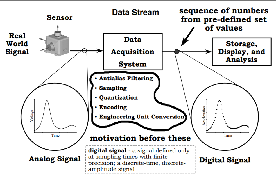
In receivers, engineers usually want to ensure that the incoming signal fits within a relatively narrow threshold for an RF ADC to accept for optimum signal conversion quality while protecting the sensitive input of the ADC from overvoltage or potentially damaging or degrading signal content outside of the desired frequency range (Figure 1).
For example, the minimum acceptable signal level for 2G cellular wireless service is −100 dBm, which equates to 1×10⁻¹³ watts or:

This is far below the acceptable voltage range for practical RF ADCs. In this case, an RF amplifier is needed, and filtering and other RF hardware may also be useful.
In the case of transmission, the transmitter power requirements may exceed the digital circuits' capability to generate adequately powered signals without RFFE power amplifiers (PAs). Modern PA design often emphasizes efficiency, and methods such as digital pre-distortion and envelope tracking, which use digital technologies alongside analog amplifier circuits, are integrated into modern PA chips to enhance efficiency. PA circuits tend to be susceptible to loading effects, which may be challenging to address with on-chip signal-generation technology. In some cases, the sheer ruggedness of the PA circuit is key, such as the ability to withstand reflections and incoming high signal power at the PA output, which is often beyond the capabilities of digital circuits used to generate RF signals at any but the lowest power levels.
How much of a system is digitized depends on the performance criteria, size, weight, power, and other system-level constraints. For RF systems with multiple RF channels, it may be beneficial to use DDC or an RF DAC and DDS to minimize the complexity of interconnects that would be involved in a fully analog system.
As a function of digital sampling and processing criteria, wider bandwidths and higher frequencies require more capable digital systems to perform DDS and DDC. Current digital hardware is capable of gigasamples per second (GSPS) rates, with specialized hardware offering up to tens of GSPS. This means that the highest-performance DDS and DDC can convert and synthesize RF signals (i.e., RF bandwidth) below 20GHz, with commercially available products typically below 15GHz of RF bandwidth. Many systems sacrifice resolution (i.e., bit count) for conversion rate to achieve higher RF bandwidth. Reduced resolution results in poorer signal quality, which is a hard constraint in many high-performance RF systems. In many cases, it is more efficient and lower cost to leverage RF hardware for frequency translation and signal conditioning to and from the digital domain beyond several gigahertz of RF bandwidth.
Digitizing much of the RF signal chain can benefit complex antenna systems and systems with extremely high numbers of RF channels. With complex antenna structures that use beamforming, beamsteering, multi-input multi-output (MIMO), or other spatial-multiplexing technologies, digitizing much of the RF signal chain may reduce the overall RF element count, size, interconnect, and power distribution.
Implementing digital RF also comes with challenges and constraints, but companies that build digital RF chips often address these challenges. These companies often provide extensive support tools and resources to aid in the development of digital RF systems using their products.
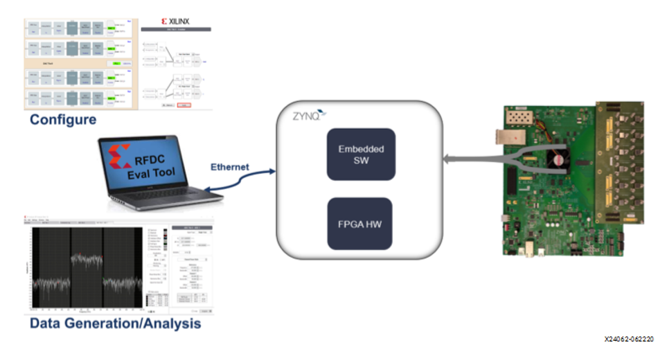
Many RF development boards come with software support, including open-source firmware, MATLAB® integration, and graphical user interfaces (GUIs) that allow users to evaluate custom waveforms and test system functionality (Figure 2). These tools may support standalone and loopback modes for ADCs and DACs and may be compatible with widely used design suites and embedded Linux platforms.
Digital RF Theory and Concepts
Engineers use digital RF technology to provide some performance, cost, or size benefit using DSP and conversion or synthesis. DSP technology, including field-programmable gate arrays (FPGAs) and dedicated digital hardware, enables precise RF signal generation, RF-to-digital conversion, digital frequency translation, and digital filtering. It also supports advanced controls like amplitude and phase adjustment and time-based signal correlation for spatial multiplexing. Some newer products can incorporate all these functions on a single chip, but many RF applications still use discrete chips for some functions, such as DDS and DDC, that are separate from the DSP. This section provides a primer on these digital RF concepts and briefly discusses how they are implemented.
Digital Sampling Theory
For an RF ADC to successfully sample an RF signal to a maximum desired frequency and resolution, the ADC must be able to sample fast enough to digitally recreate the signal features. ADCs are limited in RF bandwidth to the Nyquist criterion, which states that to accurately recreate a signal, the sample rate must be at least twice the highest-frequency component that can be accurately sampled (i.e., the Nyquist rate). That means that a 1GSPS ADC has a Nyquist frequency of 500MHz, allowing it to capture signal components up to 500MHz when sampling baseband signals.
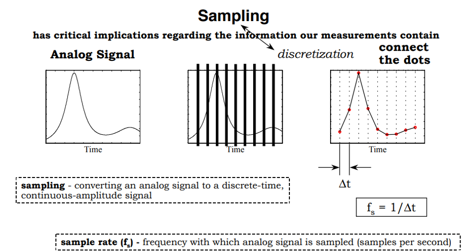
It is important to note that the sampling rate, not maximum frequency, dictates total RF bandwidth. Additionally, sections of bandwidth at higher frequencies can be sampled using downconversion. For instance, if the signal to be converted has only 10MHz of bandwidth but resides at a center frequency of 100MHz, it requires a sampling rate of 20MSPS, not 200MSPS. However, for the ADC to be able to convert that 10MHz of bandwidth, it would need to be able to sample at 210MSPS (i.e., 100MHz + 5MHz of half bandwidth) and digitally extract the desired 10MHz of bandwidth or use downconversion to extract the 10MHz bandwidth and convert it at 20Msps. Sampling rates that exceed the signal bandwidth (a technique called oversampling) can provide some benefits, such as improved signal-to-noise ratio (SNR) in the digital domain (Figure 3).
Essentially, the faster a signal is sampled, the lower the noise floor can be realized, as noise is typically spread widely over the entire sampling spectrum. With higher sampling rates, the total noise remains the same but is spread over a much wider frequency range, which can be further reduced using sampling techniques and digital filtering.
The ideal noise floor (NF) of an ADC is defined as:

This describes the level of noise quantization within the converter for a given number of bits (N) and how noise can be impacted by sampling rate (Fs) and bandwidth (BW). This equation shows that doubling the sampling rate can reduce the NF by 3dB. Combining oversampling with digital filtering can dramatically reduce the noise floor and enhance the SNR.
Another concept is undersampling, which is sampling at a much lower frequency (typically less than half) than the actual signal frequency. Undersampling can perform a conversion very similar to mixing, where the undersampled signal has frequencies that are aliased to the baseband or first Nyquist zone, like they were originally in the baseband frequency range.
However, with undersampling, a design must ensure that the wanted signals are aliased into the baseband and that the signals are in the proper spectral orientation. Undersampling can cause spectral reversal, as with mixers and lower sideband reversal. While designing a digital receiver, engineers should account for all the frequency stages, as combinations of the nonlinearity of the amplifiers and RF ADCs often result in harmonics and spur generation that can appear in the signal conversion spectrum. One way to avoid this is to select the sample rates and an intermediate frequency (IF) so that any spurs and harmonics appear out-of-band and can readily be filtered with either analog filters or digital tuners or filters.
Direct Digital Synthesis
DDS is the generation of signals, often with sub-hertz accuracy, using digital time-varying signals that are then converted to analog signals using an RF DAC. DDS can be very simple, effectively producing simple sine waves, square waves, or sawtooth waves at a wide range of frequencies. It can also be more complex, generating any signal type within the dynamic range and resolution capability of the RF DAC.
DDS allows for the generation of RF signals that exhibit excellent phase noise, low spurious content, and, depending on the design complexity, the ability to rapidly change frequency and waveforms for frequency-agile applications. It can also be used as a phase-locked loop (PLL) reference for a wide tunability range, as a local oscillator (LO) for mixing, for some modulation techniques, or to generate RF signals directly.
DDS differs from the way traditional arbitrary waveform generators (AWGs), PLLS, and frequency synthesizers generate signals. AWGs generate signals by outputting each sample of a stored waveform. Some waveform manipulation can occur using this stored method, but it is limited in frequency precision by the stored waveform and user-defined waveform functions, as AWGs only have so much memory for each sample point, and the sampling clock can only recreate a finite set of frequencies. DDS can be implemented in a variety of ways, including using a numerically controlled oscillator (NCO), a combination of phase accumulator and phase-to-amplitude converter, or asynchronous memory access. In a complex multi-channel or multi-antenna element solution, several DDS systems can be synchronized to enable advanced amplitude, phase, and waveform control.
DDS offers the following advantages:
Sub-hertz frequency accuracy and tuning
Sub-degree phase accuracy and tuning
Fast frequency-hopping speed with phase-continuous frequency hops
Elimination of overshoot/undershoot during frequency hops
No settling-time anomalies like analog hardware varieties
Fast and continuous phase tuning
Component aging, temperature drift, and other anomalies can readily be handled by digital control architecture
Digital control and software programmability allow for remote control, optimization, and automation via programmability or artificial intelligence (AI) and machine learning (ML)
However, RF DACs and DDS control systems do have limitations. Depending on the chosen code words, a phase truncation can occur and introduce errors and even spurs. Reference clock jitter, along with RF DAC quantization and linearity errors, can introduce both noise and harmonics. Some of these added spurs, harmonics, and noise can be mitigated. To help reduce undesirable signal degradation with DDS systems, engineers can select a low-phase-noise oscillator for the reference, appropriately compensate for environmental factors of jitter, use frequency division to reduce reference oscillator jitter further, use the highest possible sampling frequency to allow for oversampling, and otherwise optimize the design to minimize interference and noise in the signal path.
Digital Frequency Translation & Filtering
Digital frequency translation functions are commonly used in DSP transmitter, receiver, and transceiver applications. This approach competes with using RF mixers, doublers, and other frequency-translation hardware to upconvert or downconvert signals. However, many RF applications operate at a spectrum beyond the capability of accessible RF DACs and RF ADCs, and an analog frequency-translation stage may be necessary to convert the signal to an IF within the capability of the digital hardware. With digital frequency translation, a swath of signal bandwidth is digitized by an RF ADC and may be filtered and otherwise digitally processed to remove noise and unwanted signal content before digital downconversion to a baseband frequency for further processing and demodulation. In the case of transmission, developers can use DSP techniques to fully generate the baseband signal with modulation at extremely high fidelity, then perform digital upconversion before being synthesized using an RF DAC.
Digital frequency translation has additional nuances, such as the need to filter the unwanted image and sidebands created by the RF ADC and DDS during digital downconversion. Developers can use downsampling to help remove the unwanted frequency components created by digital downconversion outside the desired signal bandwidth. Interpolation filtering is helpful during digital upconversion, which can be achieved with a single interpolation filter but is often performed with multiple simpler interpolation filters when implemented with digital hardware such as an FPGA.
A wide variety of strategies exist to implement digital filters, which can be highly effective at mitigating spurs, noise, and harmonics. Higher-complexity digital filters provide enhanced filtering performance, but at the cost of greater hardware complexity. Therefore, it is often much more efficient to use a cascade of several simpler filter stages rather than a single complex filter stage to meet the performance goal.
For example, finite impulse response (FIR) filters and infinite impulse response (IIR) filters are often used in digital RF filtering applications. FIR filters can exhibit precise linear phases and ensure stability. They generally require linear design methods, are hardware efficient, and the filter startup transients have a finite duration. Compared with IIR filters, FIR filters typically need to be more complex to reach the same performance level but introduce a much greater delay.
Beamforming, Beamsteering, and MIMO
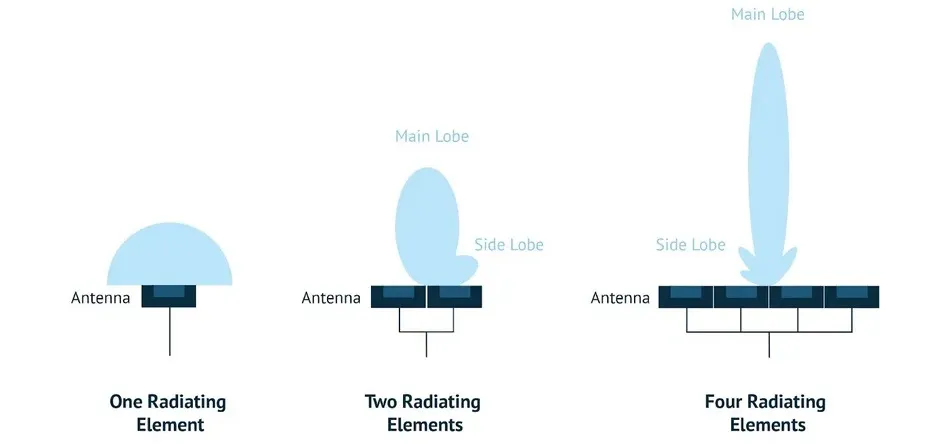
Beamforming uses multiple antenna elements in an array with coordinated phase and amplitude responses to direct the antenna pattern in a desired direction. This method uses constructive and destructive interference to form a desired antenna pattern, with lobes and nulls generated via the antenna element phase and amplitude control. Beamsteering is an advancement of beamforming where the antenna pattern is dynamically changed using the phase of the signals in real time, and not the signal path elements as with beamforming. Both techniques are used with modern, advanced communication systems, such as 5G and Wi-Fi 7.
MIMO is the use of multiple transmitter (TX) and receiver (RX) antennas to create spatial multiplexing among the various paths between the TX and RX antenna elements. Using signals within the same bandwidth that travel over different paths from TX to RX can result in redundant data transmission. The signals can carry different information to effectively multiply the throughput. The RX in a MIMO system takes advantage of the slight time difference inherent in the signals traveling along different spatial paths to differentiate the signals.
Beamforming, beamsteering, and MIMO can all be accomplished using analog methods. However, a fully analog system may not be desirable for high antenna element systems due to the resulting size, weight, power, cost, and interconnect complexity compared to a hybrid analog-digital or fully digital system (Figure 4).
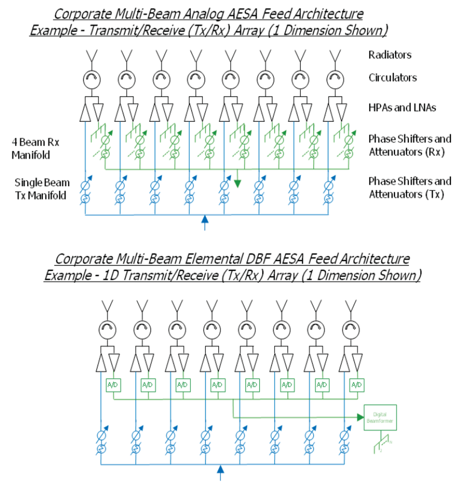
As shown in Figure 4, with a fully analog phased array, the beamforming is performed using analog phase shifters and attenuators for each element. If the received signals are digitized, the beamforming can be done in the digital domain, eliminating the need for RF phase shifters and attenuators at each element. This concept could be taken further, with the transmitter phase shifters and attenuators replaced by a digital beamformer. With appropriate DSP hardware, such a system could be used for MIMO with additional DSP techniques to perform spatial multiplexing processing.
Enabling Digital RF Connectivity with Molex Interconnect Solutions and Mouser Electronics
As digital RF architectures evolve toward higher integration and multi-channel operation, interconnect performance becomes a limiting factor in maintaining signal integrity. In hybrid and fully digital beamforming systems, precise synchronization between multiple antenna elements requires connectors and cables that can sustain low loss, consistent impedance, and minimal phase distortion across wide bandwidths.
Molex products, available through Mouser Electronics, deliver RF interconnect and cable assembly solutions designed to meet these challenges, enabling reliable performance in high-frequency digital RF systems, test setups, and advanced communication architectures.
Molex RF SMA Cable Assemblies: Versatile connectivity for high-frequency, phase-critical applications
Molex RF SMA Cable Assemblies offer flexible, high-precision connections from 0GHz to 6GHz, ensuring stable impedance and minimal signal degradation across RF channels. Their availability in multiple connector configurations, including SMA, BNC, MMCX, and Type N, enables seamless integration between the RF front end, ADC/DAC evaluation boards, and beamforming modules

These assemblies are ideal for RFFE testing, phased-array calibration, and digital RF prototyping where consistent electrical performance and mechanical reliability are essential.
Table X: Key specifications of Molex RF SMA Cable Assemblies
Specification | Details |
Frequency Range | 0GHz to 6GHz |
Impedance | 50Ω |
Voltage Rating | 500VAC (0.5mA) |
Connector Options | SMA, BNC, MMCX, Type N |
Connector Styles | Straight and right-angle |
Cable Lengths | 12" to 196" |
Applications | Commercial aviation, data/computing, MedTech, mobile devices, telecommunications |
Molex High-Speed FAKRA-Mini (HFM) Interconnect System: High-bandwidth connectivity for digital beamforming and MIMO systems
The Molex High-Speed FAKRA-Mini (HFM) Interconnect System supports frequencies up to 20GHz and data rates up to 28Gbps, making it an excellent fit for automotive radar, 5G beamforming, and digital phased-array systems. Its compact, lightweight form factor saves up to 80% board space compared to traditional FAKRA connectors, critical in multi-antenna or dense module layouts.

With ruggedized housing, integrated secondary locks (ISL), and optional connector position assurance (CPA), HFM connectors ensure stable signal transmission even in high-vibration environments.
Table X: Key specifications of Molex HFM Interconnect Systems
Specification | Details |
Frequency Range | Up to 20GHz |
Data Rate | Up to 28Gbps |
Impedance | 50Ω |
Form Factor | 80% smaller than standard FAKRA |
Operating Temperature | −40°C to +105°C |
Standards Compliance | USCAR-49, USCAR-2 |
Supported Protocols | Ethernet, MIPI A-PHY, PCIe, HDBase-T, GMSL 2/3 |
Applications | ADAS, radar, 5G, V2X, infotainment, autonomous systems |
Together, these Molex interconnect solutions help bridge digital and analog signal domains, ensuring accurate timing, amplitude, and phase relationships essential for digital beamforming, MIMO, and multi-channel RF systems.
Conclusion
Many RF systems are fully analog, but many more are in use and being developed using some digital electronics in place of RF/analog components. These newer hybrid systems are generally much more compact and, depending on the depth of digital integration, can be software programmable. Software-defined radio (SDR) and similar software programmability are incredibly versatile and allow engineers to repurpose RF hardware, reprogram it as needed, or use it in a range of different products and applications without redesigning the entire RF system.
Does this mean that RF design is becoming a matter of simply connecting an antenna to a digital front-end and programming the rest in software? This may be the case in some present and future instances where the integration of high-frequency and high-performance semiconductors or processes alongside silicon digital circuit fabrication occurs. However, there are still limitations to what can be accomplished with RF signals in the digital domain. This is why most current RF systems are still hybrid analog-digital systems.
References
[1] Kelly E. Basics of Signal Processing. In: Section 7, PIMS Data Analysis Manual. Cleveland (OH): NASA Glenn Research Center; 2003. Available from: https://gipoc.grc.nasa.gov/pims/MMAP/PIMS_ORIG/MEIT/MEIT_pdfs/meit2003/Section_7.pdf
[2] Cooley M. Phased Array-Fed Reflector (PAFR) Antenna Architectures for Space-Based Sensors. Baltimore (MD): Northrop Grumman Electronic Systems; 2015. Available from: https://ntrs.nasa.gov/api/citations/20150000333/downloads/20150000333.pdf

This article was originally published by Mouser Electronics. It has been edited by the Wevolver team and Ravi Y Rao for publication on Wevolver. Upcoming articles in this series will continue to explore key areas of RF engineering, offering engineers practical insights into the design and implementation of modern RF systems.