TPU vs GPU: Comprehensive Technical Comparison
This article explores TPU vs GPU differences in architecture, performance, energy efficiency, cost, and practical implementation, helping engineers and designers choose the right accelerator for AI workloads today!

Last updated on 02 Jul, 2026. 17 minutes read
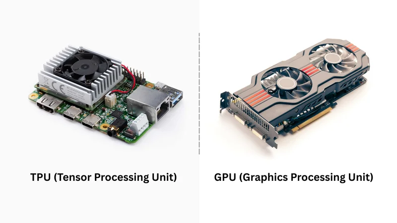
TPU vs GPU
TL; DR
TPUs are Google-designed ASICs built exclusively for neural network tensor operations, delivering superior throughput and energy efficiency for large-scale AI training and inference. GPUs are programmable parallel processors with broad framework support across CUDA, PyTorch, and OpenCL. For dedicated AI workloads at scale, TPUs win on efficiency; for flexibility, GPUs win.
Key Takeaways
Specialized vs General‑Purpose: TPUs are application‑specific integrated circuits optimized for deep‑learning tensor algebra and rely on systolic arrays for dense matrix multiplication. GPUs use thousands of programmable CUDA cores, making them flexible for graphics, scientific computing, and AI.
Energy Efficiency: For AI workloads, TPUs offer higher performance per watt, up to 2–3 times improvement over contemporary GPUs. Google’s latest Ironwood TPUs achieve roughly 30 times better efficiency than the first TPU generation.
Programming Ecosystems: TPUs are tightly integrated with Google’s TensorFlow and JAX frameworks, while GPUs support a broader ecosystem (CUDA, PyTorch, OpenCL). This affects portability and developer experience.
Use‑Case Alignment: TPUs excel at training and inference of complex neural networks, natural‑language processing, and recommendation engines. GPUs remain essential for graphics rendering, scientific simulations, and mixed workloads.
Cost and Availability: GPUs are widely available from multiple vendors and can be purchased or rented; TPUs are accessed primarily through Google Cloud, which may offer lower total cost for TensorFlow/JAX workloads but ties users to a specific ecosystem.
Introduction
In modern computing, the debate of TPU vs GPU has become central to discussions around high-performance processing, particularly in Artificial Intelligence and Machine Learning workloads. Training and deploying these models require high computational throughput. Central Processing Units (CPUs) handle general‑purpose tasks efficiently but struggle with the matrix‑heavy operations common in deep learning. The hardware accelerators that enable modern AI are Graphics Processing Units (GPUs) and Tensor Processing Units (TPUs).
GPUs, born out of computer graphics, gained popularity for scientific computing and deep learning because they contain thousands of cores that execute operations in parallel. They offer programmability and support for a wide range of algorithms and frameworks. TPUs, developed by Google as custom application‑specific integrated circuits (ASICs), target tensor algebra used in neural networks. Since the first TPU was deployed in 2016, successive generations have dramatically improved throughput and energy efficiency.
This technical comparison of TPU vs GPU explores their architectural differences, performance benchmarks, and use-case suitability. When designing advanced neural networks or running large-scale data centers, the choice of TPU vs GPU directly influences model training speed, energy consumption, and deployment strategies.
Fundamentals of GPUs and TPUs
What Is a GPU?
GPUs are specialized processors built initially to accelerate graphics rendering in video games and digital content. A modern GPU contains thousands of small cores that execute operations in parallel. Early GPUs were fixed‑function units, but the introduction of CUDA by NVIDIA in 2006 enabled general‑purpose computing on GPUs (GPGPU). [1] Today’s GPUs play a central role in AI and high‑performance computing (HPC) because they can handle large datasets, run multiple training jobs simultaneously, and execute diverse AI architectures.
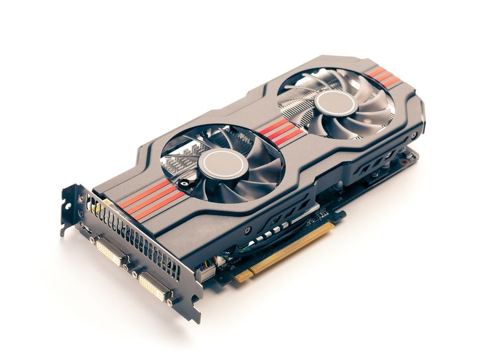
Graphics Processing Unit (GPU)
The flexibility of a GPU stems from its programmable architecture. Developers can write code using frameworks such as CUDA, OpenCL, or Vulkan, and higher-level Machine Learning libraries, such as PyTorch, Caffe, and TensorFlow, which compile down to GPU kernels. Developers can optimize GPU performance for neural network training, matrix operations, and even cryptographic algorithms.
For example, to accelerate a convolution operation on a GPU, an engineer writes a CUDA kernel that maps different pixels to different threads. The GPU scheduler orchestrates thousands of threads concurrently, delivering high throughput.
Characteristics of GPUs include:
Parallelism: Thousands of cores execute instructions concurrently. The NVIDIA H100provides up to 80 GB of high‑bandwidth memory and ~3.35 TB/s of bandwidth; the newer H200 increases this to 141 GB of HBM3e at 4.8 TB/s
Programmability: Support for general‑purpose languages like CUDA and frameworks such as PyTorch and TensorFlow.
Versatility: Suitable for graphics rendering, scientific simulations, cryptographic hashing, and deep learning.
Scalability: Multi‑GPU clusters use interconnects like NVLink or NVSwitch to connect 8–16 GPUs, enabling supercomputers such as NVIDIA DGX pods.
GPUs are ideal for general-purpose workloads, from graphics rendering to AI applications, ensuring scalability across both consumer devices and massive data centers.
Recommended Reading: Maximize GPU Utilization for Model Training: Unlocking Peak Performance
What Is a TPU?
The tensor processing unit (TPU) is a family of ASICs designed by Google to accelerate neural network training and inference. Instead of the thousands of programmable cores found in GPUs, TPUs use a systolic array architecture, in which data flows rhythmically across a grid of processing elements. Each element performs the same operation at the same time on different data points, making the chip extremely efficient at large matrix multiplications. TPUs therefore excel at convolutional and transformer workloads typical in deep learning.
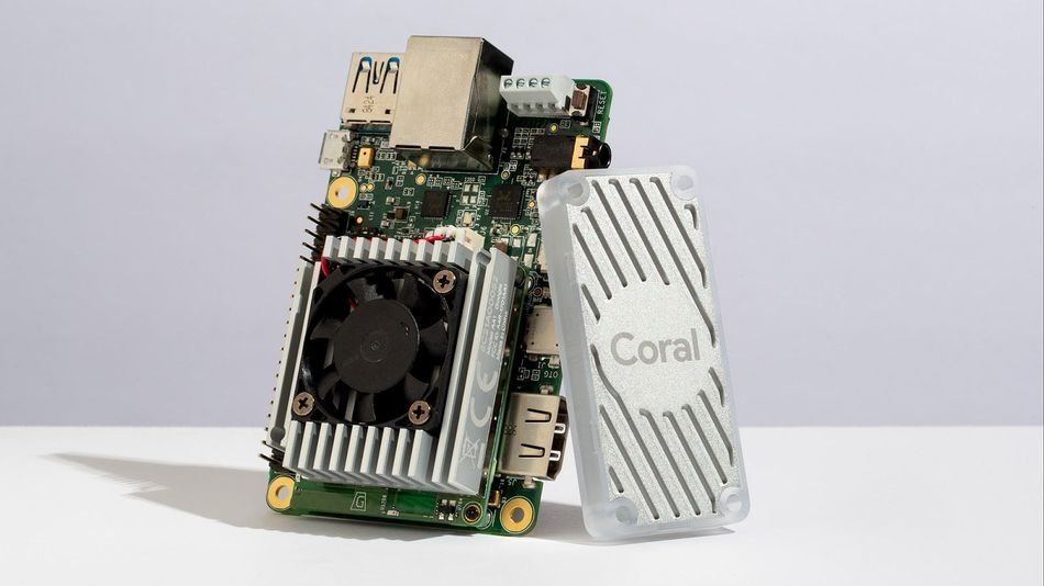
Build AI that works offline with Coral Dev Board, Edge TPU, and TensorFlow Lite
TPUs first appeared in 2016 for inference tasks. Subsequent generations added training capabilities and more memory. The current generally available TPU is Ironwood (TPU v7), which reached GA on November 6, 2025. Ironwood delivers 192 GB of high-bandwidth memory (HBM3E) at 7.37 TB/s of memory bandwidth, with pods scaling to 9,216 chips delivering 42.5 FP4 exaflops of compute. It delivers 10× the peak performance of TPU v5p and powers Google's own Gemini, Search, and YouTube workloads in production today.
Looking ahead, Google announced its eighth-generation TPUs — TPU 8t and TPU 8i — at Google Cloud Next 2026, with general availability expected later in 2026. For the first time, Google has split the generation into two purpose-built chips: TPU 8t targets large-scale model training, clustering 9,600 chips into a single superpod delivering 121 FP4 exaflops with 2 petabytes of shared HBM and targeting 2.7× better training price-performance over Ironwood. TPU 8i targets low-latency inference, carrying 288 GB of HBM alongside 384 MB of on-chip SRAM — triple the previous generation — in pods of 1,152 chips delivering 11.6 exaflops, with 80% better inference price-performance than Ironwood. Both chips deliver up to 2× better performance per watt than Ironwood and run natively on JAX, PyTorch, vLLM, and XLA.
Unlike GPUs, TPUs are tightly integrated with TensorFlow, JAX, and the Google Cloud ecosystem, requiring code compilation via the XLA compiler for optimized execution.
Characteristics of TPUs include:
Systolic Arrays: Fixed-function matrices optimized for dense matrix multiplications
High Performance Per Watt: TPU 8t and 8i deliver up to 2× better performance per watt than Ironwood, which itself delivers 10× the peak performance of TPU v5p.
Deep Integration with TensorFlow and JAX: TPUs run on the XLA compiler by Google and require code to be compiled for the TPU target. Their software stack includes TensorFlow TPU, JAX, PyTorch (now in native preview), vLLM, and the Pathways runtime.
Limited Generality: TPUs lack the flexibility of GPUs; they primarily target AI workloads and are available mainly through Google Cloud.
TPUs provide energy efficiency and high performance for AI workloads, but their limited versatility means they primarily serve specific tasks in the Google Cloud ecosystem.
Recommended Reading: FPGA Architecture: A Comprehensive Guide for Digital Design Engineers
Evolution of TPU Generations
Google has released several TPU generations, each improving performance, scalability, and energy efficiency. The table below summarizes key improvements from the first TPU in 2016 through the eighth generation announced in 2026. . The notable innovations include liquid cooling, large-scale pods, and increasingly high-end memory bandwidth.
Generation | Year | Focus | Notable Improvements |
TPU v1 | 2016 | Inference | First ASIC for Neural Network Inference, Internal to Google |
TPU v2 | 2017 | Training & Inference | Added Support for Training and Launched Publicly via Google Cloud |
TPU v3 | 2018 | Training Scale | Introduced Liquid Cooling and Pods for Large Scale Training |
TPU v4 | 2021 | Efficiency | Increased Memory and Energy Efficiency; each Pod provides up to 1.1 exaflops |
TPU v5e/p | 2023 | Cost Optimized Training | Supports up to 8,960 Chips per Pod and Uses Liquid Cooling |
Trillium (v6e) | 2024 | Performance Jump | 4.7× Faster than v5e; 32 GB HBM per chip at ~1,600 GB/s; 67% more energy-efficient than v5e |
Ironwood (v7) | 2025 | Inference‑First Design | 192 GB HBM per Chip, 7.2 TB/s bandwidth, 42.5 Exaflop Pods, ~2× perf/watt vs Trillium |
TPU 8t | 2026 | Large-Scale Training | 9,600-chip superpod; 121 FP4 exaflops; 2 PB shared HBM; 2.7× training price-performance over Ironwood; GA later 2026 |
TPU 8i | 2026 | Low-Latency Inference | 1,152-chip pods; 11.6 exaflops; 288 GB HBM + 384 MB on-chip SRAM; 80% better inference price-performance over Ironwood; GA later 2026 |
Each TPU generation refined acceleration, energy efficiency, and scalability, solidifying TPUs as leading application-specific integrated circuits for AI workloads, especially in large-scale model training and inference within Google Cloud.
Architectural Differences
Compute Design: CUDA Cores vs Systolic Arrays
GPUs rely on thousands of programmable CUDA cores operating under the Single Instruction Multiple Threads (SIMT) model, where one instruction is issued to a warp of 32 threads simultaneously — delivering broad parallelism across general-purpose workloads. [2] This versatility allows engineers to run graphics rendering, scientific computing, and AI tasks efficiently. Developers exploit GPU parallelism through frameworks such as CUDA, cuBLAS, and cuDNN, or rely on PyTorch and TensorFlow for neural network training. However, performance can degrade when irregular datasets or memory access patterns limit core utilization.
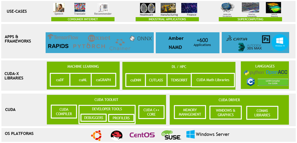
CUDA Applications and Libraries; Source: NVIDIA
TPUs adopt a different approach with systolic arrays. Data streams through grids of multiply-accumulate (MAC) units, enabling extremely efficient tensor operations and matrix multiplications. This fixed-function design minimizes memory fetches and control overhead, resulting in superior energy efficiency and throughput. The trade-off is reduced flexibility; TPUs are optimized for AI workloads but cannot efficiently execute arbitrary algorithms or broad general-purpose computing tasks.
The table below compares CUDA cores (SIMT) vs TPU systolic arrays across key architectural dimensions:
Attribute | GPU (CUDA Cores) | TPU (Systolic Arrays) |
Design Purpose | General‑Purpose Parallelism | Matrix/Tensor Operation Efficiency |
Programmability | High; Supports CUDA, OpenCL, GLSL, and ML frameworks | Low; Compiled via XLA for TensorFlow/JAX |
Peak Utilization | Depends on Workload; Irregular Patterns can reduce Utilization | High for Dense Matrix Operations |
Flexibility | Suitable for AI, Graphics, Simulations, and Cryptography | Optimized for AI workloads; Limited Generality |
GPUs prioritize versatility and programmability, while TPUs sacrifice flexibility for optimized acceleration of AI workloads, offering superior throughput and energy efficiency in dense neural network training.
Recommended Reading: Understanding Nvidia CUDA Cores: A Comprehensive Guide
Memory Hierarchy and Bandwidth
Memory bandwidth is critical for deep learning because large tensors must be moved quickly between memory and compute units. GPUs typically use high‑bandwidth memory (HBM) and a hierarchical cache (global, shared, and texture caches) to maximize throughput. For example, the H100 includes up to 80 GB of HBM3 memory and 3.35 TB/s of memory bandwidth, the H200 upgrades this to 141 GB of HBM3e at 4.8 TB/s — nearly double the capacity and 1.4× the bandwidth of the H100. . GPUs rely on interconnects such as NVLink (NVLink 4.0 at 900 GB/s bidirectional per GPU) and NVSwitch to scale to multiple GPUs.
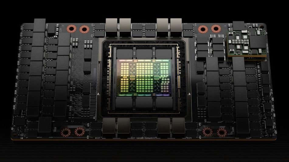
H100 Tensor Core GPU by NVIDIA
TPUs integrate HBM directly on-die, reducing memory controller overhead and improving latency. Ironwood features 192 GB of HBM per chip and 7.37 TB/s of memory bandwidth, more than double that of the H100. The custom Inter‑Chip Interconnect (ICI) by Google provides 9.6 Tb/s per chip , enabling tight synchronization across thousands of chips with low latency. This integration reduces the need for separate memory controllers and decreases energy consumption, significantly lowering overall power consumption.
Interconnects and Scalability
Scalability is achieved by connecting multiple chips via high‑speed interconnects. In GPU clusters, NVLink/NVSwitch enables 8–16 GPUs per node with up to 900 GB/s bandwidth. Systems like the DGX H100 scale to ~512–1,024 GPUs, reaching a peak compute capability of about 1 exaflop. However, heterogeneous workloads may face scheduling complexity.
TPU pods use ICI by Google, allowing up to 9,216 Ironwood chips in a single pod. This design yields 42.5 exaflops of compute power and low network latency. The eighth-generation TPU 8t scales further to 9,600 chips per superpod, delivering 121 FP4 exaflops with 2 PB of shared HBM. The synchronous design ensures that all chips remain in lock‑step, which simplifies scheduling but reduces flexibility for heterogeneous workloads.
Precision and Numeric Formats
Deep learning performance often depends on numeric precision. GPUs support floating‑point precision (FP32, FP16, BF16) and lower‑precision formats like INT8 and FP8. [3] Mixed‑precision training uses Tensor Cores (e.g., in Hopper by NVIDIA and Blackwell architectures) to improve throughput. The Blackwell B200 extends this further with FP4 and FP6 support, reaching up to 18 PFLOPS of sparse FP4 throughput. GPUs excel at tasks requiring high precision; scientific simulations and HPC workloads rely on FP64 arithmetic.
TPUs emphasize lower precision to boost performance per watt. Most TPUs operate on bfloat16 (BF16) or INT8 values, sacrificing some numerical accuracy for speed. This trade‑off is acceptable for many AI workloads where the model can tolerate quantization errors. However, tasks requiring double precision are not a good fit for TPUs.
GPUs remain the standard for high-performance computing requiring precision, while TPUs excel in AI workloads, trading accuracy for energy efficiency and speed in large-scale deep learning tasks.
Recommended Reading: Tensor Cores vs CUDA Cores: The Powerhouses of GPU Computing from Nvidia
Performance Comparison
Throughput and Training Time
Throughput is often measured in tera‑floating‑point operations per second (TFLOPS). According to a comparative analysis report, Google’s TPU v4 delivers up to 275 TFLOPS, while NVIDIA's H100 provides 1,979 TFLOPS FP16 dense (3,958 TFLOPS sparse), and the Blackwell B200 delivers 4,500 TFLOPS FP8 dense and 9,000 TFLOPS FP4 dense — roughly 4× the H100's AI compute throughput for training workloads. For mixed-precision tasks, the TPU v5e achieves 460 TFLOPS**; Ironwood (TPU v7) reaches 4,614 TFLOPS per chip.
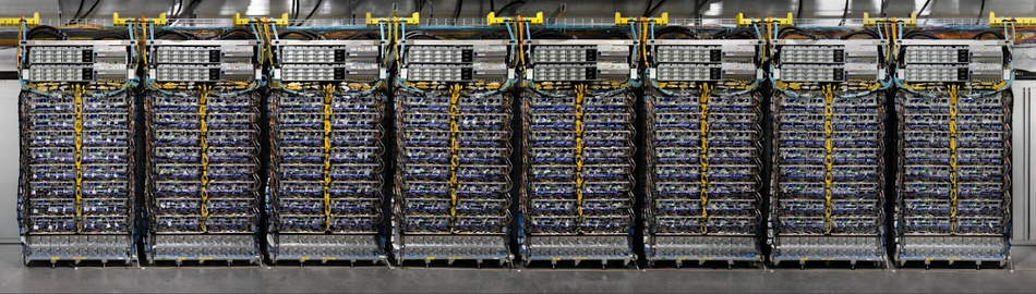
TPU v4 enables Performance, Energy, and CO2e Efficiency Gains. Source: Google
The training time depends on model size and hardware efficiency. The same report notes that TPU v3 trained BERT models 8× faster than NVIDIA - V100 and delivered 1.7–2.4× faster training times for ResNet‑50 and large language models. These speedups arise from the TPUs’ dense matrix multipliers and optimized interconnects.
Inference Performance
Inference tasks benefit from specialized hardware and lower precision. Ironwood TPUs support inference at scale with 4,614 TFLOPS per chip, 192 GB memory, and 7.37 TB/s bandwidth. Pods scale to 9,216 chips (42.5 exaflops) with low latency. Google’s TPU v4i provides 137 TOPS per inference slice and can process 400–1,000 frames per second with 0.5‑watt Edge TPUs.
GPUs, optimized with TensorRT, also excel at inference. The B200 delivers approximately 17,500 tokens per second on Llama 70B in FP4 versus the H100's ~3,000 tokens per second — a roughly 5× throughput advantage for large-model inference. They remain highly effective for AI workloads, especially when tuned for specific datasets and frameworks. However, GPUs generally consume more power and require manual optimization to match TPU-level efficiency.
Performance Per Watt
Energy efficiency is critical in data centers and embedded devices. TPUs usually deliver 2–3× better performance per watt compared to GPUs. The B200 consumes 1,000W TDP, a 43% increase over the H100/H200's 700W; though it delivers roughly 4× the compute, improving performance per watt on transformer workloads. Google’s Ironwood design is nearly 30× more efficient than the first TPU generation. GPUs remain powerful but consume more energy; energy‑saving techniques such as dynamic voltage and frequency scaling (DVFS), pruning, and quantization are necessary to optimize their performance‑per‑watt. Even so, GPUs cannot yet match TPU levels of energy efficiency, particularly at large-scale deployments.
Scalability and Peak Compute
In multi‑chip environments, TPUs scale more aggressively than GPUs. Ironwood pods support 9,216 chips, delivering 42.5 exaflops. TPU 8t superpod scales to 9,600 chips delivering 121 FP4 exaflops with 2 PB of shared HBM. In contrast, GPU clusters typically support a few hundred GPUs; the DGX H100 system provides roughly 1 exaflop of peak compute, while the GB200 NVL72 — a full rack of 72 Blackwell GPUs — delivers 720 petaFLOPS FP4 and is available today. TPU pods use synchronous communication across ICI, resulting in low latency and high throughput. GPU clusters rely on NVLink/NVSwitch with moderate network latency but offer a more flexible topology.
Cost, Market Share, and Availability
TPUs are available primarily as cloud services. Google’s Cloud TPU offers per‑second billing and can be more cost‑efficient for TensorFlow workloads. ByteBridge’s report notes that TPUs can be 4–10× more cost‑effective for large‑scale language model training and provide 1.2–1.7× better performance per dollar compared with NVIDIA’s A100 GPUs. TPUs also consume 30–50 % less power, reducing cooling and maintenance costs.
GPUs dominate the market with roughly 80% share of AI accelerator deployments; TPUs account for about 3–4%. H100 cloud pricing has fallen to $2–$3.50/hr on major platforms as supply has increased; B200 instances are available from select providers at approximately $4.99–$6.03/hr on demand as of mid-2026. GPUs are widely accessible for purchase or rental and support diverse frameworks, making them the default choice for many researchers and enterprises. TPUs tie users to Google Cloud, limiting hardware customization but providing integrated software and infrastructure support.
TPUs offer superior price-to-performance for AI workloads on Google Cloud, while GPUs dominate globally through broad ecosystem compatibility and unmatched market availability.
Recommended Reading: NPU vs GPU: Understanding the Key Differences and Use Cases
Use Cases and Application Suitability
When to Choose TPUs?
TPUs shine in workloads where dense matrix operations and high throughput dominate. Common applications include:
Image Classification and Computer Vision: Convolutional neural networks (CNNs) require heavy matrix multiplications. TPUs accelerate convolution layers and dense layers, enabling fast inference for object detection and segmentation.
Natural Language Processing (NLP): Transformers and language models like BERT benefit from the ability of TPUs to process large batches of sequences efficiently. Google’s BERT training uses TPUs for faster convergence.
Recommendation Systems: TPUs handle massive embedding tables, image recognition tasks, and dense matrix computations found in recommendation algorithms.
Large Language Models (LLMs): Google’s Gemini and Gemma, as well as competitors like Claude models, rely on pods of TPUs for training and deployment.
Research in Federated Learning and On‑Device AI: Smaller, energy‑efficient TPUs enable edge inference and federated learning with high privacy.
TPUs are the clear choice for large-scale AI tasks such as LLMs, CNNs, and NLP models, where energy efficiency and matrix acceleration dominate.
When to Choose GPUs?
GPUs remain indispensable for applications beyond deep learning. It is better to choose GPUs when:
Graphics Rendering and Gaming: The original purpose of the GPU remains relevant for rendering realistic graphics, ray tracing, and virtual reality.
Scientific Simulations: Physics, chemistry, and climate models rely on double precision and complex algorithms, which GPUs handle well.
Cryptocurrency Mining: Cryptographic hashing tasks map well to GPU parallelism.
General AI Research: GPUs support frameworks like PyTorch and custom CUDA kernels, making them ideal for prototyping new architectures.
Mixed Workloads: When an organization runs AI alongside rendering, video encoding, or HPC tasks, GPUs provide the necessary flexibility.
GPUs dominate in general-purpose computing, making them essential for scientific computing, simulations, rendering, and mixed AI workloads requiring versatility and framework compatibility.
Hybrid Approaches
Many organizations use a hybrid strategy: training models on GPUs for flexibility and prototyping, then deploying inference on TPUs for production efficiency.
Research Labs: Prefer GPUs due to PyTorch’s dynamic graphs and broad ecosystem.
Production Systems: Favor TPUs for scalability, energy efficiency, and seamless Google Cloud integration.
Heterogeneous Systems: Combine CPUs, GPUs, and TPUs, assigning specific tasks to the most suitable hardware for optimal performance.
The hybrid model maximizes strengths — GPUs for flexibility and prototyping, TPUs for scalable deployment, ensuring efficiency across research, production, and real-world AI workloads.
Recommended Reading: Understanding Nvidia CUDA Cores: A Comprehensive Guide for 2026
Practical Implementation Considerations
Programming and Toolchains
GPUs support multiple programming models, with CUDA (NVIDIA), HIP (AMD), and OpenCL offering access to their general-purpose parallel processing capabilities. High-level frameworks such as PyTorch, TensorFlow, and JAX simplify development while enabling custom kernel optimization for specific tasks. This flexibility makes GPUs suitable for AI models, graphics rendering, and scientific computing workloads.
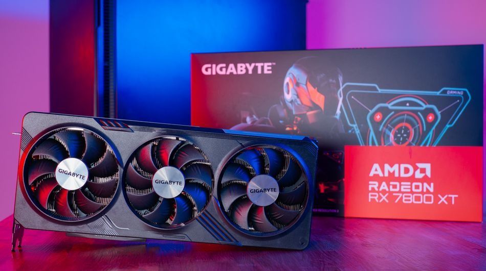
Gigabyte Radeon RX 7800 XT Gaming OC 16GB
TPUs, in contrast, are tightly integrated with TensorFlow and JAX through the XLA compiler, which fuses operations and distributes them across systolic arrays. PyTorch on TPUs is now supported in native preview via PyTorch/XLA, though highly optimized neural network workloads remain the primary use case. TPUs offer limited compatibility with custom frameworks, and deferred execution can make debugging more complex.
Memory and Data Movement
Memory bandwidth and data transfer patterns directly impact accelerator efficiency. GPUs employ high-bandwidth memory (HBM), hierarchical caches, and pinned host memory with asynchronous streams to maximize throughput. Unified memory simplifies management but may introduce latency overhead in large-scale workloads.
On TPUs, data pipelines must feed systolic arrays continuously to avoid stalls. Prefetching and efficient partitioning are critical for scaling neural network training. For massive datasets, frameworks like GSPMD and JAX's pjit manage model parallelism, enabling large deep learning models to span multiple chips.
Deployment and Infrastructure
GPUs offer deployment flexibility across on-premises clusters, co-location facilities, and cloud environments. Their ecosystem compatibility supports varied use cases from video games to machine learning workloads.
TPUs are primarily available through Google Cloud, where integration with AI frameworks like TensorFlow and JAX delivers efficiency. Engineers must weigh latency, cost, and data sovereignty in choosing infrastructure.
Both accelerators demand robust cooling systems and significant power capacity. Liquid cooling is standard for dense TPU pods and advanced GPU clusters. The B200 GPU operates at 1,000W TDP and requires liquid cooling or rear-door heat exchangers in dense rack configurations. Scalability differs; GPUs scale moderately via NVLink and InfiniBand, while TPUs achieve extreme scalability through synchronized pod architectures.
Hardware Design Insights for Digital Designers
Digital design engineers may be involved in designing custom ASICs or integrating accelerators into systems. The lessons from TPUs and GPUs include:
ASIC vs Programmable Logic: TPUs demonstrate the power of ASICs tailored to specific workloads. Systolic arrays require careful timing and data flow control to avoid stalls. FPGA implementations of systolic arrays can prototype designs before committing to silicon.
High Bandwidth Memory Integration: Co‑locating HBM with compute fabric minimizes latency. Packaging technologies like 2.5D integration (silicon interposers) enable high‑density memory stacks. Engineers must balance thermal constraints and signal integrity.
Interconnect Design: Large‑scale systems require high‑speed interconnects (e.g., ICI, NVLink). Engineers must design protocols that balance bandwidth, latency, and energy. Serializing data across multiple differential pairs introduces clock‑domain synchronization challenges.
Precision Selection: Choosing numeric formats (BF16, FP16, FP8, FP4, INT8) impacts accuracy, memory usage, and energy. Hardware designers implement multiple data paths or configurable quantization units to support mixed precision.
Error Detection and Fault Tolerance: As chip counts grow, soft errors become common. Techniques such as ECC memory, parity bits, and redundancy ensure reliability in TPU pods and GPU clusters.
Hardware designers can learn from GPU versatility and TPU specialization, applying insights on memory, interconnects, and precision to build future-ready high-performance accelerators.
Recommended Reading: The Technological Enablers of Edge AI | The 2025 Edge AI Technology Report
Cost Considerations and Economic Analysis
The cost influences hardware selection. The factors include capital expenditure (CAPEX), operational expenditure (OPEX), and total cost of ownership (TCO).
Capital Expenditure (CAPEX): GPUs can be purchased outright for on‑premises clusters or rented from multiple cloud providers. TPUs are only available via Google Cloud; however, Google began offering direct enterprise TPU sales in 2025, with Anthropic among the first customers to deploy on-premises TPU infrastructure, which reduces upfront cost but limits hardware control.
Operational Expenditure (OPEX): Energy consumption and cooling are significant. TPUs often provide better performance per watt, lowering power bills. The B200 GPU operates at 1,000W TDP — 43% higher than the H100/H200 — though its 4× compute improvement narrows the performance-per-watt gap for large-model workloads. GPU costs vary by vendor; the latest H200 or Blackwell chips command premium prices but support various workloads.
Total Cost of Ownership (TCO): Reports indicate that TPUs provide 1.2–1.7× better performance per dollar for large‑scale Machine Learning tasks and reduce total costs by 20–30 % due to lower energy and cooling requirements. However, overall economics depend heavily on workload compatibility, developer expertise, and reliance on different frameworks.
TPUs often achieve lower TCO for large-scale AI workloads, though GPUs remain cost-effective for organizations prioritizing ecosystem compatibility and broader general-purpose computing tasks.
Future Trends and Innovations
GPU Innovations
GPUs are evolving rapidly to support diverse AI applications and general-purpose computing tasks. The NVIDIA H200 integrates 141 GB of HBM3e memory with 4.8 TB/s bandwidth and NVLink 4.0 at 900 GB/s per GPU. The Blackwell B200 (now shipping from major cloud providers in 2025–2026) delivers 4,500 TFLOPS FP8 dense and 9,000 TFLOPS FP4 dense — roughly 4× the AI compute throughput of the H100 — with 192 GB HBM3e at ~8 TB/s bandwidth.
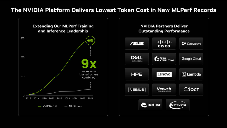
Future GPUs will combine ray-tracing cores, tensor cores, and integrated AI accelerators, extending their versatility beyond graphics rendering into real-time inference and large-scale scientific computing.
TPU Innovations
Google’s TPU roadmap prioritizes scalability and energy efficiency for AI workloads. Trillium (v6) improved efficiency by 4.7× compared to v5e, while Ironwood (v7) enables real-time reasoning for Gemini and AlphaFold with pods scaling to 42.5 exaflops. The eighth-generation TPU 8t and TPU 8i were announced at Google Cloud Next 2026, targeting large-scale training and low-latency inference, respectively, with GA expected later in 2026. Google's Axion, its custom Arm Neoverse v2 CPU, now complements TPUs within the AI Hypercomputer stack for host-side workloads. Edge TPUs are shrinking in size, enabling on-device AI for IoT, smartphones, and autonomous systems—expanding TPU adoption into low-latency applications outside hyperscale data centers.
Market Dynamics
The AI accelerator market is estimated to reach USD 249 billion by 2030, growing at a CAGR of approximately 37% from USD 52 billion in 2025. NVIDIA leads with approximately 80–92% market share in AI accelerator chips, supported by its dominant CUDA software ecosystem. Revenue share peaked near 87% in 2024 and is projected to decline toward 75% by 2026 as competitors scale. Competitors like AMD's MI300X and Intel's Gaudi3 are entering with hybrid architectures that combine GPU programmability with TPU-style tensor operations, targeting large-scale AI workloads. TPUs maintain a smaller but expanding footprint, expected to dominate inference at hyperscale and specialized AI applications, particularly within Google Cloud.
Conclusion
GPUs and TPUs both accelerate AI workloads, yet their strengths lie in different domains. GPUs offer unmatched flexibility, ecosystem compatibility, and support for diverse computing tasks such as graphics rendering, simulations, and AI research. TPUs, built with systolic arrays, excel in deep learning models, providing superior throughput and energy efficiency, though with reduced generality. The right choice depends on factors like architecture, cost, scalability, and framework support. For TensorFlow and JAX workloads in Google Cloud, TPUs deliver excellent cost-efficiency, while GPUs remain the preferred option for mixed workloads and local deployments. Looking ahead, innovations in performance per watt, memory bandwidth, and numeric precision will further expand the boundaries of AI hardware acceleration.
Frequently Asked Questions (FAQs)
1. What is the fundamental difference between a GPU and a TPU?
A. GPUs are programmable processors designed for parallel computing, capable of running diverse open-source frameworks such as PyTorch and TensorFlow. TPUs, built by Google, focus on tensor operations, accelerating AI workloads with systolic arrays.
2. Are TPUs always faster than GPUs?
A. No. TPUs provide superior parallel computing efficiency for TensorFlow workloads, often outperforming GPUs in large-scale training. However, GPUs may perform better in tasks requiring open-source flexibility, precision, or non-AI computing tasks.
3. Can I run PyTorch code on a TPU?
A. Yes. You can run PyTorch code on a TPU using PyTorch/XLA, which enables PyTorch models to execute on TPU hardware
4. How do TPUs achieve higher energy efficiency?
A. TPUs use a systolic array architecture that streams data through fixed multiply-accumulate (MAC) units with minimal memory fetches and control overhead. This fixed-function design, combined with native lower-precision formats like BF16 and INT8, delivers significantly higher performance per watt than general-purpose GPU cores.
5. Which hardware should I choose for a new AI project?
A. Select GPUs if you need open-source flexibility, multiple frameworks, or mixed parallel computing tasks. Choose TPUs if your workload is TensorFlow-centric and deployed on Google Cloud for cost-efficiency.
6. Do TPUs replace GPUs in the long term?
A. No. TPUs complement GPUs rather than replace them. GPUs dominate open-source ecosystems and parallel computing versatility, while TPUs target specialized AI workloads at scale. Hybrid adoption will remain common.
References
[1] ResearchGate. Architectural evolution of NVIDIA GPUs for High-Performance Computing [Cited 2026 June 30]. Available at: Link
[2] ResearchGate. Introduction to GPU Computing and CUDA Programming: Case Study on FDTD [Cited 2026 June 30]. Available at: Link
[3] Nvidia. Floating-Point 8: An Introduction to Efficient, Lower-Precision AI Training [Cited 2026 June 30]. Available at: Link
[4] Mordor Intelligence. AI Accelerators Market Size & Share Analysis - Growth Trends and Forecast (2025 - 2030) [Cited 2026 June 30]. Available at: Link
in this article
1. Key Takeaways2. Introduction3. Fundamentals of GPUs and TPUs4. Architectural Differences5. Performance Comparison6. Use Cases and Application Suitability7. Practical Implementation Considerations8. Cost Considerations and Economic Analysis9. Future Trends and Innovations10. Conclusion11. Frequently Asked Questions (FAQs)12. References