Schmitt Trigger: Robust Comparator Design with Hysteresis
A Schmitt trigger is a comparator circuit with built-in hysteresis that uses two switching thresholds to eliminate noise and ensure stable output transitions. It is widely used for signal conditioning, waveform shaping, and robust digital and analog circuit design.

27 Jul, 2026. 17 minutes read
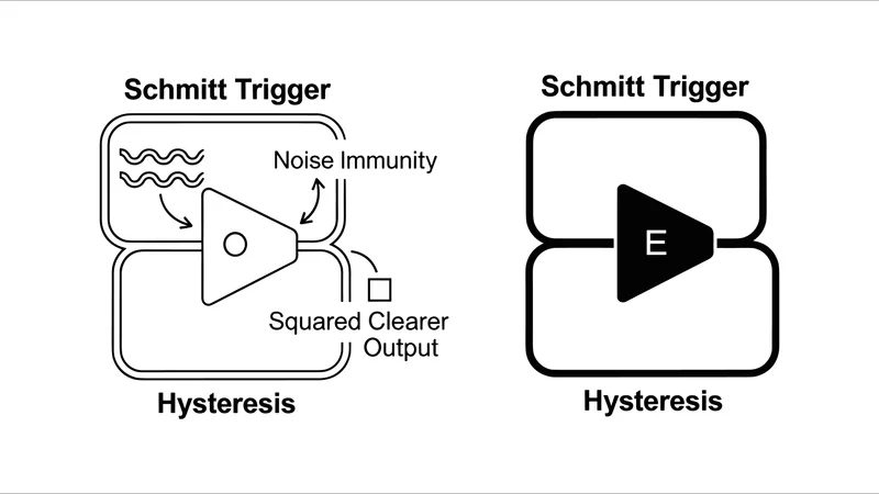
Schmitt Trigger Input
Key Takeaways
● A Schmitt trigger is a comparator with built-in hysteresis. Positive feedback ensures the output toggles only when the input crosses distinct upper (V(TH)) and lower (V(TL)) threshold voltages, so noise within the hysteresis window cannot cause repeated toggles.
● Inverting op-amp Schmitt trigger thresholds. With input resistor R1, feedback resistor R2, and saturation voltage V(sat), the thresholds are V(TH) = (R1 / (R1 + R2)) × V(sat) and V(TL) = (R1 / (R1 + R2)) × (−V(sat)). The hysteresis width is V(H) = V(TH) − V(TL) = (2 × R1 / (R1 + R2)) × |V(sat)|
● Non-inverting Schmitt trigger. Using superposition, V(UT) = +(R1 / R(f)) × V(sat) and V(LT) = −(R1 / R(f)) × V(sat). The hysteresis is 2 × (R1 / R(f)) × |V(sat)|
● Discrete BJT Schmitt trigger. Two transistors sharing a common emitter resistor produce hysteresis because the emitter voltage shifts with the output state. Typical resistor values give roughly 0.4 V of hysteresis.
● CMOS Schmitt-trigger inverters. The SN74HC14 at 4.5 V supply has a typical positive threshold V(T+) of about 2.5 V and negative threshold V(T−) of about 1.6 V; hysteresis ranges from about 0.4 V to 2.1 V The single-gate SN74LVC1G14 supports 1.65-5.5 V supplies; at 5.5 V, typical V(T+) is 2.61-3.33 V and V(T⁻) is 1.87-2.29 V, giving 0.71-1.11 V of hysteresis.
● Comparator ICs with hysteresis. The LM393 dual comparator operates from 2-36 V with a large-signal response of roughly 300 ns and a small-signal response of 1.3 µs [5]. The TLV3201 micropower comparator has a 40 ns propagation delay and 1.2 mV of built-in internal hysteresis, operating from 2.7 to 5.5 V.
Introduction: Why Add Hysteresis to a Comparator?
Standard comparators switch output state whenever the input crosses a reference voltage. When a noisy input or a slowly varying analog signal hovers near that reference, the comparator output can chatter, rapidly toggling high and low as noise causes repeated threshold crossings. This behavior is problematic in digital circuits and sensor interfaces because it generates multiple unwanted transitions, wastes power, and can create false triggers. Otto Schmitt first addressed this issue in 1934 while working to measure neuronal signals: he added positive feedback to an amplifier so that the circuit switched at different threshold levels depending on whether the input was rising or falling, creating a bistable transfer curve. The resulting Schmitt trigger produces a clean digital output even when the input has slow edges or significant noise.
Hysteresis is essential in many embedded systems: it debounces mechanical switches, shapes waveforms, prevents oscillation when sampling analog levels, and enables simple oscillators. This article provides a detailed engineering reference on Schmitt trigger design. It explores the principles of hysteresis and derives the threshold voltages for inverting and non-inverting op-amp comparators, examines discrete transistor implementations, and compares integrated CMOS Schmitt-trigger inverters (74HC14, SN74LVC1G14, CD40106/MC14584). It also discusses comparator ICs with adjustable hysteresis and presents practical applications such as debouncing, zero-cross detection, and relaxation oscillators.
Recommended reading: How to Read Electrical Schematics: A Comprehensive Guide for Engineers
Deriving the Thresholds
Consider the op-amp output at its positive saturation +V(sat). The voltage divider formed by R1 and R2 sets the non-inverting input voltage, and when the inverting input, V(IN), crosses this divider voltage, the output flips. Solving the divider math gives:
V(TH) = (R1 / (R1 + R2)) × V(sat)
When the op-amp saturates at −V(sat), the same analysis yields:
V(TL) = (R1 / (R1 + R2)) × (−V(sat))
The hysteresis voltage is the difference between the two thresholds:
V(H) = V(TH) − V(TL) = (2 × R1 / (R1 + R2)) × |V(sat)|
These formulas match those found in many electronics textbooks: the threshold voltages scale directly with the resistor divider ratio. Note that the magnitude of V(sat) depends on the op-amp's supply rails and its saturation characteristics; practical op-amps saturate at slightly less than the rails, so the actual thresholds may be slightly lower than calculated.
Design Example
Suppose an inverting Schmitt trigger uses ±5 V supply rails with V(sat) approximately 4.5 V. Choosing R1 = 10 kΩ and R2 = 30 kΩ gives R1 / (R1 + R2) = 0.25, so V(TH) is approximately +1.13 V and V(TL) is approximately −1.13 V, giving a hysteresis V(H) of about 2.25 V. To reduce the hysteresis, decrease R1 relative to R2. Always ensure the threshold band is wider than the maximum expected noise amplitude to prevent chatter.
Non-Inverting Schmitt Trigger
A non-inverting Schmitt trigger uses positive feedback to prevent output chatter. When the input signal crosses the upper threshold, the output switches high, and it remains high until the input drops below the lower threshold, ensuring clean digital transitions.
Circuit Configuration
In the non-inverting Schmitt trigger, the input is applied to the non-inverting terminal of the op-amp through resistor R1, while the inverting terminal is connected to ground or a reference. Feedback resistor R(f) connects the output back to the non-inverting input. Positive feedback still occurs, but the polarity is reversed: when the output is high, the feedback raises the threshold, and when the output is low, the feedback lowers it. This configuration is useful when the reference is ground, and the output must swing between ±V(sat). This op-amp topology is a close cousin of the difference amplifier, which uses a similar resistor network to combine two input signals rather than to create hysteresis.
Recommended reading: Difference Amplifier: Theory, Design, and Applications for Engineers
Threshold Derivation
Using superposition, the voltage at the non-inverting input, V(+), is the sum of contributions from the input and the feedback voltage. Setting V(+) equal to the inverting reference (ground) at the switching point and solving gives:
V(LT) = −(R1 / R(f)) × V(sat) V(UT) = +(R1 / R(f)) × V(sat)
The hysteresis width is V(H) = V(UT) − V(LT) = 2 × (R1 / R(f)) × |V(sat)|. Note that the threshold signs are opposite those of the inverting configuration because the input is non-inverting. This configuration is popular for zero-cross detectors and sine-to-square converters, where the threshold is symmetric around zero.
Setting Specific Thresholds
If the desired upper threshold is V(UT) and the lower threshold is −V(UT) (symmetrical), the ratio R1 / R(f) should equal V(UT) / V(sat). For example, for ±5 V supply rails (V(sat) approximately 4.5 V) and desired thresholds at ±1 V, choose R1 / R(f) = 0.22, then select convenient resistor values such as R1 = 22 kΩ and R(f) = 100 kΩ. For thresholds offset from zero, such as detecting a positive voltage level, bias the inverting input at a reference voltage and derive new expressions for V(TH) and V(TL) accordingly.
Choosing the Hysteresis and Resistor Values
When designing a Schmitt trigger, the hysteresis width should exceed the maximum expected amplitude of input noise but remain small enough to preserve sensitivity. Large hysteresis improves noise immunity but increases propagation delay and may distort the conversion of analog waveforms, while too little hysteresis allows noise to cause chattering. The table below summarizes the key considerations when selecting resistor values.
Design Factor | Guidance |
Hysteresis width | Set by R1/(R1+R2) for inverting designs or R1/Rf for non-inverting designs. Larger ratios give larger hysteresis. For sensors with ±100 mV of noise, design VH to be at least ±200 mV. In integrated inverters, hysteresis is fixed by device geometry. |
Input bias currents | Real op-amps and comparators have finite bias currents and input offset voltages. Keep resistor values in the 10 kΩ to 100 kΩ range to minimize their effect on the threshold voltage. |
Output drive | Comparators with open-collector outputs (e.g., LM393) require a pull-up resistor. Its value, together with the load capacitance, sets the propagation delay; too large a pull-up slows the rising edge. |
Reference voltage | For single-supply circuits that must detect input levels above ground, bias the inverting input to a reference (e.g., half the supply) using a resistor divider, and update the VTH/VTL equations to include that reference. |
Discrete BJT Schmitt Trigger
The discrete BJT Schmitt trigger is a circuit that uses bipolar junction transistors to create a switching action with hysteresis, useful for signal conditioning.
Two-Transistor Emitter-Coupled Circuit
A classic transistor-based Schmitt trigger uses two bipolar junction transistors (BJTs) with their emitters tied together through a resistor R(E) and their collectors each driving complementary output nodes. One transistor, Q1, receives the input signal at its base; the other, Q2, forms positive feedback by connecting its collector back to the base of Q1 through a resistor. When V(IN) is low, Q1 is off, and Q2 is on, pulling the output low; when V(IN) is high enough to turn Q1 on, the voltage drop across R(E) increases, turning Q2 off and letting the output rise. The hysteresis arises because turning Q1 on or off changes the emitter voltage, altering the base-emitter voltage needed for switching.
Operating Principle
With Q2 on and the output low, the emitter node sits at a voltage set by the current through R(E). The input must exceed approximately 0.6 V plus this emitter voltage to turn Q1 on. Once Q1 turns on and pulls Q2 off, the emitter node drops toward ground, so to switch back, the input must fall to approximately 0.6 V above the new, lower emitter voltage. The upper and lower thresholds therefore differ by the change in emitter voltage, which equals the current through R(E) multiplied by its resistance; adjusting R(E) or the collector resistors changes the hysteresis. In practice, small-signal transistors with R(E) of a few hundred ohms yield hysteresis of roughly 0.3-0.5 V, suitable for TTL-level signals. Designers must size the transistor currents appropriately: too large a current reduces hysteresis, and too small a current can cause the circuit to oscillate.
Design Example
Consider a discrete Schmitt trigger using NPN BJTs with R(C1) and R(C2) at 10 kΩ, R(E) at 1 kΩ, and feedback resistor R(F) at 100 kΩ. When the input rises, Q1 turns on at around 0.6 V above the emitter voltage. Suppose the emitter current when Q2 is on is 1 mA; the emitter voltage is then 1 mA × 1 kΩ = 1 V, so the input must exceed approximately 1.6 V to switch the output high. After switching, the emitter current falls to about 0.1 mA, and the emitter voltage drops to about 0.1 V, so the input must fall below approximately 0.7 V to switch low. The resulting hysteresis is approximately 0.9 V, and adjusting R(E) allows the hysteresis window to be tailored to the application.
Integrated CMOS Schmitt-Trigger
An integrated CMOS Schmitt trigger is a compact circuit built with complementary metal-oxide-semiconductor technology, designed for reliable signal switching with hysteresis.
Inverters
Discrete transistor circuits are bulky and require biasing. Modern logic families instead build Schmitt trigger behavior directly into compact CMOS logic gates, providing fixed hysteresis and fast switching that make them ideal for digital interfacing and waveform conditioning.
Recommended reading: Understanding Logic Gate Symbols: A Comprehensive Guide for Engineers
SN74HC14 (HC Logic Family)
The SN74HC14 is a hex inverter with Schmitt trigger inputs. It operates from 2-6 V supplies and offers high noise immunity. The datasheet lists the positive-going switching threshold V(T+) and negative-going threshold V(T−) across supply voltages: at V(CC) = 4.5 V, V(T+) typical is 2.5 V (max 3.13 V) and V(T−) typical is 1.6 V (max 2.45 V), so the hysteresis delta V(T) ranges from 0.4 V to 2.1 V. At V(CC) = 2 V, the thresholds scale down accordingly. Propagation delay is modest: at 4.5 V, the typical t(pd) is about 12 ns and the maximum is 25 ns. Because the thresholds are relatively wide and scale with supply voltage, this device suits cleaning up slow edges and noisy signals in 5 V logic systems.
Recommended reading: VSS vs VDD: Understanding Power Rails in Electronic Circuit Design
SN74LVC1G14 (LVC Logic Family)
Texas Instruments' SN74LVC1G14 is a single Schmitt-trigger inverter in a tiny package. It operates from 1.65 V to 5.5 V and offers ±24 mA of output drive. The datasheet emphasizes distinct positive-going (V(T+)) and negative-going (V(T−)) thresholds to provide hysteresis. At V(CC) = 5.5 V, the positive-going threshold is 2.61-3.33 V, and the negative-going threshold is 1.87-2.29 V, giving a hysteresis of 0.71-1.11 V. At V(CC) = 3 V, V(T+) is 1.5-1.87 V and V(T−) is 0.84-1.16 V, with hysteresis of 0.56-0.87 V. Propagation delay at 3.3 V is typically 1.5 ns and no more than 4.6 ns, making this device well suited to interfacing with microcontrollers and FPGAs.
CD40106 / MC14584 (4000-Series CMOS)
The CD40106B, also sold as the MC14584B, is a six-stage CMOS Schmitt-trigger inverter that operates over a wide supply range of 3-18 V. It offers larger hysteresis than 74HC devices, making it suitable for high-noise environments or slow analog waveforms. According to the datasheet, at V(DD) = 5 V, the positive trigger threshold V(P) ranges from about 2.2 V to 3.6 V, and the negative trigger threshold V(N) ranges from 0.9 V to 2.8 V. The hysteresis voltage V(H) can be as high as 1.6 V at 5 V and 3.5 V at 15 V. These large margins let the CD40106 reject significant noise, though propagation delay is higher, typically tens of nanoseconds, because of the higher supply voltages and larger device geometry.
MC74HC14A (HCT Variant)
Onsemi's MC74HC14A is a 74HC14 variant with TTL-compatible input thresholds in the HCT family. The datasheet indicates that at a V(CC) of approximately 5 V, the positive-going threshold V(T+) can vary between roughly 1.2 V and 2.1 V, while the negative-going threshold V(T−) lies between about 0.5 V and 1.4 V; hysteresis spans 0.4-1.5 V across temperature. These TTL-compatible thresholds make the MC74HC14A useful when interfacing CMOS logic with legacy 5 V TTL devices.
The table below compares the four CMOS Schmitt-trigger inverters.
Device | Supply range | VT+ / VT− (typical, 5 V) | Hysteresis | Propagation delay |
SN74HC14 | 2–6 V | 2.5 V / 1.6 V | 0.4–2.1 V | ~12 ns typ. at 4.5 V |
SN74LVC1G14 | 1.65–5.5 V | 2.61–3.33 V / 1.87–2.29 V (at 5.5 V) | 0.71–1.11 V | 1.5 ns typ. at 3.3 V |
CD40106 / MC14584 | 3–18 V | 2.2–3.6 V / 0.9–2.8 V | Up to 1.6 V at 5 V; 3.5 V at 15 V | Tens of ns |
MC74HC14A | ~5 V (TTL) | 1.2–2.1 V / 0.5–1.4 V | 0.4–1.5 V across temperature. | Comparable to 74HC14 |
Comparator ICs With Hysteresis
These ICs are specialized chips that compare two input voltages, featuring built-in hysteresis to prevent rapid switching and noise sensitivity.
LM393 With External Hysteresis
The LM393 is a dual, low-offset voltage comparator designed for reliable operation over a wide supply-voltage range. It operates from a single supply of 2 V to 36 V or dual supplies up to ±18 V, while consuming only about 0.4 mA of typical supply current. These features make it well suited for low-power applications, instrumentation systems, and sensor interface circuits that require accurate voltage comparison.
The LM393 does not include built-in hysteresis. Therefore, an external feedback resistor, R(H), is typically connected between the comparator output and the non-inverting input (or reference node) to introduce positive feedback. This positive feedback creates two different switching thresholds: one for a rising input voltage and another for a falling input voltage. For example, the comparator may switch from low to high when the input exceeds 2.7 V and switch back from high to low only after the input drops below 2.3 V, creating a 0.4 V hysteresis window. This separation between the switching thresholds prevents the output from rapidly toggling in response to small input fluctuations or electrical noise, resulting in more stable and reliable operation.
The LM393 features an open-collector output, meaning it cannot drive the output to the high state on its own. Consequently, an external pull-up resistor is required. A value of approximately 4.7 kΩ is commonly used because it provides a good balance between fast output rise times and low power consumption, although the exact value may be adjusted to suit the supply voltage and load requirements.
TLV3201: Micropower Comparator With Internal Hysteresis
TI's TLV3201 is a single high-speed, low-power comparator designed for battery-powered systems. It operates on 2.7-5.5 V supplies and features a propagation delay of 40 ns with only 40 µA of supply current. Crucially, it includes 1.2 mV of internal hysteresis for improved noise immunity; this very small hysteresis prevents oscillation when the input is near the threshold but is too small to interfere with typical high-speed signals. The comparator is rail-to-rail, and its input common-mode range extends 200 mV beyond either supply, allowing detection of near-rail signals. Designers can add external hysteresis using resistors to enlarge the trip window, making the TLV3201 well suited to high-speed pulse-width-modulation monitoring, zero-cross detection, and level translation in mixed-signal systems.
Applications
Schmitt triggers are widely used in debouncing mechanical switches, squaring noisy analog waveforms (like sine waves), and clean zero-crossing detection. They also act as relaxation oscillators to generate square waves and condition sensor signal inputs.
Switch Debouncing
Mechanical switches and pushbuttons often bounce, creating multiple rapid on/off transitions when pressed or released. A simple RC filter followed by a Schmitt-trigger inverter eliminates the bounce. The RC time constant should exceed the mechanical bounce duration, for example 10 ms; a 10 kΩ resistor in series with a 1 µF capacitor yields exactly that. When connected to a 74HC14 input, the capacitor slowly charges and discharges, and the inverter's hysteresis ensures that noise or residual oscillation on the RC node does not toggle the output until the voltage has definitively passed the threshold. Digital designers who prefer a clock-synchronous approach sometimes debounce with an SR latch instead, sampled on a clock edge; in high-reliability designs, using two stages of Schmitt-trigger inverters and a pull-down resistor to discharge the capacitor further improves noise margin.
Recommended reading: Understanding the SR Latch: Theory, Design, Truth Tables, and Practical Implementations
Zero-Cross Detection and Signal Squaring
Many AC measurement systems need to detect when a sinusoidal signal crosses zero. A non-inverting Schmitt trigger comparator can perform this task. For symmetrical detection, set the thresholds at ±V(UT) around zero using equal resistor ratios as derived earlier. For example, to detect zero crossings of a 5 V(pp) sine wave with ±50 mV of noise, choose V(H) = 200 mV; with ±5 V supply rails and ±4.5 V saturation, the resistor ratio R1 / R(f) should satisfy 2 × (R1 / R(f)) × V(sat) ≈ 0.2 V, which solves to R1 / R(f) ≈ 0.022. Selecting R1 = 2.2 kΩ and R(f) = 100 kΩ gives thresholds at ±100 mV. A comparator such as the TLV3201, or an op-amp with high slew rate and internal hysteresis, is ideal for fast zero-cross detection.
A Schmitt trigger is also used to square up the output of sensors or oscillators. Converting a triangle or sine wave into a clean square wave for digital processing requires a comparator with hysteresis; without it, the output would jitter around the crossing points.
Relaxation Oscillator
A relaxation oscillator uses a Schmitt-trigger inverter and an RC network to produce a periodic square wave. Connecting a resistor R and capacitor C between the inverter's output and input creates a timing network: when the output is high, the capacitor charges toward V(CC) through R, and when the voltage on the capacitor reaches the upper threshold V(T+), the inverter output toggles low, causing the capacitor to discharge toward ground until it crosses the lower threshold V(T−). The cycle then repeats. The oscillation period T depends on R, C, and the threshold voltages:
T = R × C × ln((V(CC) − V(TL)) / (V(CC) − V(TH))) + R × C × ln(V(TH) / V(TL))
For integrated devices like the SN74HC14 or SN74LVC1G14, the thresholds are fixed, so designers choose R and C to set the desired frequency; a typical application uses R between 10 kΩ and 1 MΩ and C between 100 pF and 1 µF. Designers who need adjustable frequency and duty cycle without relying on a fixed-threshold inverter often reach for a dedicated 555 timer instead. Be sure to account for variation in threshold voltages due to supply voltage and temperature; larger hysteresis reduces duty-cycle variation but increases propagation delay, which lengthens the oscillation period.
Recommended reading: 555 Timer Circuit: Theory and Practice for Modern Engineers
Sensor Signal Conditioning and Level Translation
Many sensors output slowly varying voltages that may be noisy or have a poor slew rate. Feeding such signals directly into digital logic can cause erratic behavior. A Schmitt trigger cleans up the waveform, ensuring clean rising and falling edges. Additionally, comparators with adjustable hysteresis can translate analogue levels to logic thresholds; for example, using a voltage divider to set the threshold and adding positive feedback creates a window comparator that only toggles when the sensor output moves outside a specified range. This is useful for battery voltage monitoring, temperature threshold detection and tamper detection. In noisier environments, designers often precede the comparator with an active low pass filter to attenuate high-frequency noise before it reaches the Schmitt trigger input.
Recommended reading: Active Low Pass Filter Design and Implementation
Common Mistakes
The most common design error is omitting positive feedback altogether: simply connecting an op-amp as a bare comparator invites chattering whenever the input is noisy or has slow edges, so always add positive feedback or choose an integrated Schmitt-trigger device instead. A closely related mistake is setting the hysteresis too small; if V(H) is smaller than the expected noise amplitude, the circuit defeats its own purpose and can still produce multiple toggles, so hysteresis should comfortably exceed the worst-case noise plus margin.
On single-supply systems, forgetting to bias the comparator's non-inverting input is another frequent problem: the threshold ends up sitting at ground, which can saturate the output and cause latch-up, so use a voltage divider or reference IC to set the desired switching point. Using a general-purpose op-amp as a comparator is also risky, since most op-amps are not optimized for open-loop switching, saturate slowly, and may have output stage issues; dedicated comparators such as the LM393 or TLV3201 are designed to switch quickly and handle large input differentials, so check the slew rate and output drive limitations before substituting an op-amp.
Finally, two supporting details are easy to overlook. Comparators with open-collector or open-drain outputs, such as the LM393, require a pull-up resistor; without one, the output can float and produce undefined logic levels. And noise on the supply rails can modulate the thresholds of an integrated Schmitt-trigger inverter, so always bypass V(CC) to ground with capacitors and follow the manufacturer's layout guidelines.
Conclusion
A Schmitt trigger is a fundamental building block that converts analog signals into clean digital levels while rejecting noise. Its hallmark is hysteresis, the separation between the switching thresholds for rising and falling inputs, and understanding the underlying resistor networks and device characteristics enables engineers to design reliable interfaces, oscillators, and waveform conditioners.
This article surveyed inverting and non-inverting op-amp implementations, analyzed discrete transistor-based Schmitt triggers, and compared integrated CMOS devices such as the SN74HC14, SN74LVC1G14, and CD40106. Comparators like the LM393 require external feedback resistors to implement hysteresis, whereas modern devices like the TLV3201 include small internal hysteresis. Applications range from switch debouncing and zero-cross detection to relaxation oscillators and sensor conditioning.
Looking forward, ultra-low-power Schmitt triggers are becoming increasingly important in IoT sensor nodes and wearable devices, where leakage currents and sub-threshold operation must be carefully managed. Some modern comparators now offer programmable hysteresis, allowing software control of threshold levels for adaptive noise filtering. As mixed-signal systems continue to proliferate, mastering Schmitt trigger design remains an essential skill for hardware and analog engineers.
FAQ
What is a Schmitt trigger, and how does it work?
A Schmitt trigger is a comparator with positive feedback that provides two distinct switching thresholds. When the input voltage rises above the upper threshold V(TH), the output switches, and it remains in that state until the input falls below the lower threshold V(TL). The difference V(H) = V(TH) − V(TL) is called hysteresis, and this arrangement prevents output chatter when the input crosses the threshold multiple times.
What is the difference between a comparator and a Schmitt trigger?
A bare comparator switches output when the input crosses a single reference, so small noise near the threshold can cause multiple toggles. A Schmitt trigger adds positive feedback so that the switching threshold depends on the output state; the resulting hysteresis provides noise immunity and well-defined switching points.
How do I calculate hysteresis voltage?
For an inverting op-amp Schmitt trigger with input resistor R1, feedback resistor R2, and saturation voltage V(sat), the thresholds are V(TH) = (R1 / (R1 + R2)) × V(sat) and V(TL) = −(R1 / (R1 + R2)) × V(sat). The hysteresis width is V(H) = V(TH) − V(TL) = (2 × R1 / (R1 + R2)) × |V(sat)|. For non-inverting triggers, the ratio R1 / R(f) sets the hysteresis instead.
When should I use a 74HC14 versus an op-amp Schmitt trigger?
Use an integrated CMOS Schmitt-trigger inverter, such as the 74HC14 or SN74LVC1G14, for digital interfacing, waveform shaping, and simple oscillators; these devices offer fixed hysteresis and fast switching down to nanoseconds with no external components. Use an op-amp or comparator instead when thresholds need to be adjustable, when working with analog signal levels, or when the supply range exceeds the limits of CMOS logic families.
How do I debounce a switch using a Schmitt trigger?
Connect a resistor and capacitor in series between the switch and ground, and connect the junction to a Schmitt-trigger inverter input. Choose the RC time constant to be longer than the expected bounce duration, for example, 10 ms. The inverter's hysteresis ensures that the output only toggles when the capacitor voltage crosses the upper or lower threshold, eliminating spurious transitions.
Can a Schmitt trigger be used as an oscillator?
Yes. A relaxation oscillator uses a Schmitt-trigger inverter with an RC network between output and input; the capacitor alternately charges and discharges between the thresholds, creating a square wave. The period is T = R × C × ln((V(CC) − V(TL)) / (V(CC) − V(TH))) + R × C × ln(V(TH) / V(TL)), and adjusting R and C sets the frequency.
What is the difference between inverting and non-inverting Schmitt triggers?
In an inverting Schmitt trigger, the input is applied to the inverting terminal of the op-amp or comparator, and the output signal is inverted relative to the input; the thresholds depend on the ratio R1 / (R1 + R2). In a non-inverting Schmitt trigger, the input is applied to the non-inverting terminal, the output is not inverted, and the thresholds depend on the ratio R1 / Rf. The choice affects the polarity of the switching points and is determined by the application.
How much hysteresis should I add?
The hysteresis should be larger than the maximum anticipated noise or ripple on the input. If the noise amplitude is ±50 mV, design V(H) to be at least ±100 mV. Excessive hysteresis may reduce sensitivity or delay switching, so select values that balance noise immunity against response speed, and when using integrated devices, choose a part whose hysteresis range matches your signal amplitude.
References
- P. Horowitz and W. Hill, The Art of Electronics, 3rd ed. Cambridge, U.K.: Cambridge University Press, 2015.
- A. S. Sedra, K. C. Smith, T. C. Carusone, and V. Gaudet, Microelectronic Circuits, 8th ed. New York, NY, USA: Oxford University Press, 2021.
- Texas Instruments, "Understanding Schmitt Triggers," Application Brief SCEA046, Dallas, TX, USA. [Online]. Available: https://www.ti.com/document-viewer/lit/html/SCEA046
- R. Moghimi, "Curing Comparator Instability with Hysteresis," Analog Dialogue, Analog Devices, vol. 34, no. 3. [Online]. Available: https://www.analog.com/en/resources/analog-dialogue/articles/curing-comparator-instability-with-hysteresis.html
- I. M. Filanovsky and H. Baltes, "CMOS Schmitt trigger design," IEEE Transactions on Circuits and Systems I: Fundamental Theory and Applications, vol. 41, no. 1, pp. 46–49, Jan. 1994.
in this article
1. Key Takeaways2. Introduction: Why Add Hysteresis to a Comparator?3. Non-Inverting Schmitt Trigger4. Threshold Derivation5. Setting Specific Thresholds6. Choosing the Hysteresis and Resistor Values7. Discrete BJT Schmitt Trigger8. Operating Principle9. Design Example10. Integrated CMOS Schmitt-Trigger11. Comparator ICs With Hysteresis12. Applications13. Zero-Cross Detection and Signal Squaring14. Relaxation Oscillator15. Sensor Signal Conditioning and Level Translation16. Common Mistakes17. Conclusion18. FAQ19. References