LM358 Op Amp: Pinout, Specs & Circuit Guide
The LM358 is a dual operational amplifier that runs from a single power supply and senses all the way down to ground. This guide covers the pinout, specs that actually constrain your design, the output stage behaviour that catches engineers out, and worked circuit examples.

10 Aug, 2026. 16 minutes read
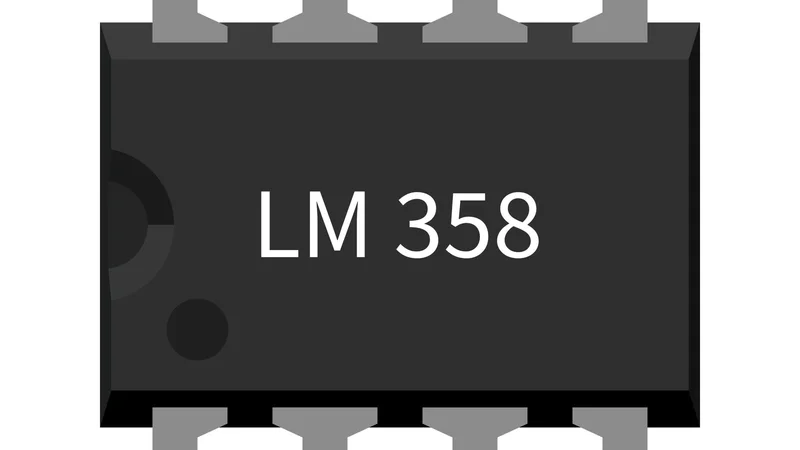
LM358 Dual Operational Amplifier
Key Takeaways
The LM358 packs two independent op amps into an 8-pin package and operates from a single supply of 3 V to 30 V, or from split supplies, with a common-mode input voltage range that includes the negative rail.
LM358 output can pull to within 20 mV of the negative rail under light loads, but positive-rail headroom is far less generous; up to 1.5 V short of V+ at a 5 V supply with light loads, widening to 2 to 4 V short of V+ at higher supply voltages or heavier loads.
The output stage has no class AB bias, so it produces crossover distortion near ground unless you add a pull-down resistor from the output to the negative supply.
With a 0.7 MHz gain bandwidth product and a 0.3 V/µs slew rate, the LM358 suits DC and low-frequency signal conditioning, not audio-grade or high-speed work.
The newer LM358B raises the supply range to 36 V, the unity-gain bandwidth to 1.2 MHz, and ESD immunity to 2 kV HBM, while cutting quiescent current to 300 µA per amplifier.
Introduction
The LM358 IC is one of the most widely second-sourced analog parts in electronics. National Semiconductor introduced the design in the mid-1970s, and Texas Instruments has manufactured the LM358 since acquiring National Semiconductor in 2011; the current TI datasheet revision still carries the original SLOS068 document number.
Its appeal is specific. Before parts like this, using an op amp on a single 5 V rail meant awkward biasing, because older devices such as the LM741 needed the input to stay several volts away from either rail.
The LM358 removed that constraint. Its inputs and output both work down to the negative rail, so a 5 V digital system can do analog signal conditioning without generating a negative supply.
This guide works through the LM358 pin configuration, the datasheet specifications that matter in practice, single-supply biasing, the output stage limitation, and concrete circuits you can build.
What Is the LM358 IC?
The LM358 is a dual operational amplifier IC containing two independent, high-gain op amps in a single 8-pin package. It operates from a single supply (3V–30V), and its input and output range extends down to ground, making it ideal for single-supply signal conditioning circuits. Split-supply operation also works, provided the total difference between supplies stays within the rated range, and VS sits at least 1.5 V above the input common-mode voltage. 1
The low supply-current drain is independent of the magnitude of the supply voltage. That property matters for battery-powered instruments, where you want the same quiescent current at 24 V as at 5 V.
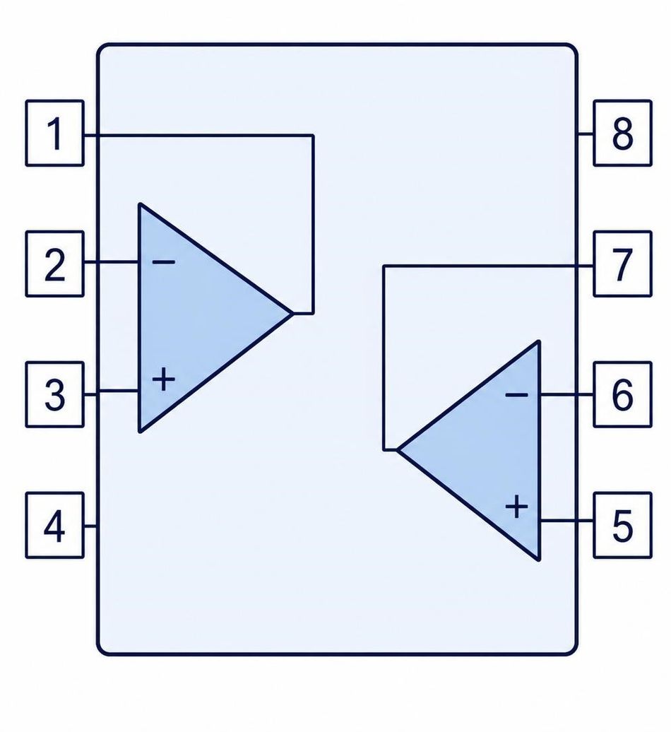
At 350 µA per amplifier, its low power consumption is modest enough for always-on sensing circuits that must not drain a battery between service intervals.
TI lists its intended applications as transducer amplifiers, DC gain blocks, and conventional op amp circuits implemented in single-supply systems. 1 Named end applications include motor control across AC induction, brushed DC, brushless DC, and stepper types; power supplies and mobile chargers; uninterruptible power supplies; and white goods such as washers, dryers, and refrigerators.
Recommended Reading: Brushless vs Brushed Motor: Engineering Trade-offs and Design Decisions
The LM358 Family: LM158, LM258, LM2904
The LM158, LM258, LM358, and LM2904 belong to the same dual operational amplifier family. They share the same basic architecture and pinout but are offered in different grades, primarily distinguished by their operating temperature range, supply-voltage rating, and electrical performance specifications. 1
Device | Operating ambient temperature | Supply voltage range |
LM158, LM158A | -55 °C to 125 °C | 3 V to 30 V |
LM258, LM258A | -20°C to 85 °C | 3 V to 30 V |
LM358, LM358A | 0 °C to 70 °C | 3 V to 30 V |
LM358B, LM358BA | -40 °C to 85 °C | 3 V to 36 V |
LM2904 | -40 °C to 125 °C | 3 V to 26 V |
LM2904B, LM2904BA | -40 °C to 125 °C | 3 V to 36 V |
The temperature ratings are taken from TI’s official datasheet. 1
If your product sees automotive or outdoor temperatures, the commercial-grade LM358 at 0 °C to 70 °C is the wrong choice. Instead, use an LM2904 or LM358B variant with an operating temperature range that matches your application's requirements, rather than relying on operation outside the device's specified ratings.
Recommended Reading: How Does a DC Motor Work? Unveiling the Power Behind Electric Motion
LM358 Pinout and Pin Configuration
The LM358 family is available in several package options, including PDIP, SOIC, TSSOP, VSSOP, SO, SOT-23-8, and CDIP. Regardless of package, the logical pin functions remain the same when viewed from the top. 1
Pin | Name | Function |
1 | OUT1 | Output, amplifier 1 |
2 | IN1- | Inverting input, amplifier 1 |
3 | IN1+ | Non-inverting input, amplifier 1 |
4 | V- | Negative supply (V−) or ground in single-supply operation |
5 | IN2+ | Non-inverting input, amplifier 2 |
6 | IN2- | Inverting input, amplifier 2 |
7 | OUT2 | Output, amplifier 2 |
8 | V+ | Positive supply |
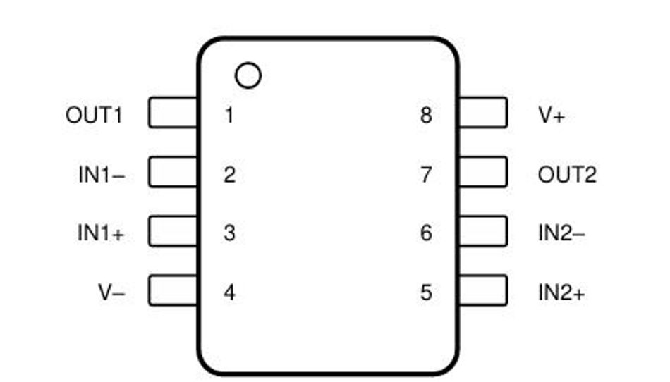
Two details trip people up. There is no offset null pin, unlike the LM741, so you cannot trim offset at the device. The two amplifiers share the same power supply pins (V+ and V−) but otherwise have independent signal paths, contributing to a typical channel separation of 120 dB (1 kHz–20 kHz)
Note that the pin order runs output-first on amplifier 1 (pins 1, 2, 3) and input-first on amplifier 2 (pins 5, 6, 7). The layout is mirrored, not repeated, which is a common source of prototyping errors.
Package Options and Part Number Suffixes
Texas Instruments identifies the package type using a package suffix within the LM358 part number. 1 Common package options and their body sizes are listed below.
Part number | Package | Body size |
LM358P | PDIP-8 | 9.81 mm × 9.43 mm |
LM358D | SOIC-8 | 4.9 mm × 6 mm |
LM358PW | TSSOP-8 | 3 mm × 6.4 mm |
LM358DGK | VSSOP-8 | 3 mm × 4.9 mm |
LM358BDDF | SOT-23-8 | 2.9 mm × 2.8 mm |
LM358PS | SO-8 | 6.2 mm × 7.8 mm |
For breadboard and through-hole work, the LM358P in PDIP-8 is the usual choice. For surface-mount production, SOIC-8 is one of the most commonly used package options because it balances ease of assembly with compact size. The LM358B is also available in a compact SOT-23-8 package with roughly 90% less package body area than the PDIP-8 version.
You will also encounter LM358N in distributor catalogs. The "N" suffix is commonly used by several second-source manufacturers, including STMicroelectronics and onsemi, to denote the PDIP-8 package. Although these devices are pin-compatible, always verify the datasheet for the specific manufacturer you are purchasing from, as electrical characteristics such as input offset voltage, input bias current, slew rate, and operating temperature range may differ.
LM358 Datasheet Specifications
These are the classic LM358 numbers at VS = 5 V and 25 °C, alongside the newer LM358B. 1
Parameter | LM358 | LM358B | Notes |
Supply voltage range | 3 V to 30 V | 3 V to 36 V | Single or split |
Input offset voltage | 3 mV typ, 7 mV max | 0.3 mV typ, 3 mV max | LM358A: 2 mV typ, 3 mV max |
Input bias current | -20 nA typ, -250 nA max | -10 nA typ, -35 nA max | Flows out of the inputs |
Input offset current | 2 nA typ, 50 nA max | 0.5 nA typ, 4 nA max | At 25 °C |
Gain bandwidth product | 0.7 MHz | 1.2 MHz | Trade-off: usable bandwidth = GBW ÷ closed-loop gain |
Slew rate | 0.3 V/µs | 0.5 V/µs | Unity gain |
Open-loop voltage gain | 25 V/mV min, 100 V/mV typ | 70 V/mV min, 140 V/mV typ | VS = 15 V, RL ≥ 2 kΩ (LM358), RL ≥ 10 kΩ (LM358B) |
CMRR | 65 dB min, 80 dB typ | 20 µV/V typ, 100 µV/V max | B version specified as a ratio, not in dB |
PSRR | 65 dB min, 100 dB typ | 2 µV/V typ, 15 µV/V max | B version specified as a ratio, not in dB |
Quiescent current per amplifier | 350 µA typ, 600 µA max | 300 µA typ, 460 µA max | VS = 5 V |
Input voltage noise density | 40 nV/√Hz | 40 nV/√Hz | At 1 kHz |
ESD, human body model | ±500 V | ±2000 V | Per ANSI/ESDA/JEDEC JS-001 |
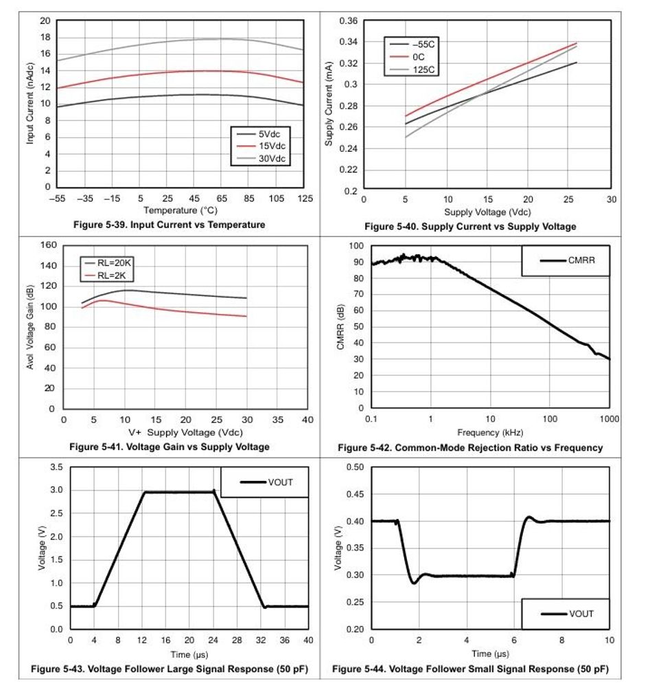
The B version is worth specifying on new designs. It raises unity-gain bandwidth by about 70%, to 1.2 MHz, cuts typical offset by an order of magnitude, adds an internal RF and EMI filter, and quadruples ESD immunity, all at lower quiescent current for genuinely low power consumption.
Supply and Common-Mode Input Voltage Range
The valid common-mode input voltage range runs from the negative rail up to VS minus 1.5 V at 25 °C, narrowing to VS minus 2 V across the full temperature range.
On a 5 V single supply, that means inputs are valid from 0 V to about 3.5 V at room temperature, and only to 3 V across temperature. Signals above that are outside the guaranteed range.
Three behaviours deserve attention. The inputs may exceed the positive supply without immediate damage, provided the absolute maximum input-voltage rating is not exceeded. However, operation outside the specified common-mode range is not guaranteed. At least one input must sit inside the valid common-mode range for the output to have the correct phase, and if both inputs leave the range, the output phase is undefined. If either input goes more than 0.3 V below V-, limit the input current to 1 mA.
Absolute maximum ratings for the classic LM358 are ±16 V or 32 V total supply, ±32 V differential input, and -0.3 V to 32 V at either input. Output short circuits to ground last indefinitely at or below 25 °C with VS ≤ 15 V, but shorts to the supply rail cause excessive heating and eventual destruction.
Output Voltage Swing
The asymmetry in the output voltage swing is the single most important practical characteristic of this part.
Condition | Swing limit |
Toward ground, VS = 5 V, RL ≤ 10 kΩ | Within 5 mV typ, 20 mV max of V- |
Toward positive rail, VS = 5 V, RL ≥ 2 kΩ | up to 1.5V below V+ (max) |
Toward positive rail, VS = 30 V, RL ≥ 10 kΩ | Stops 2 V typ, 3 V max below V+ |
Toward positive rail, VS = 30 V, RL = 2 kΩ | Up to 4 V below V+ (worst case) |
The LM358 is not a rail-to-rail op amp. On a 5 V rail driving 2 kΩ, your usable output window is roughly 0 V to 3.5 V, so a full-scale 0 V to 5 V output is not achievable.
Output current capability is also asymmetric. The device sources 20 mA minimum and 30 mA typical, but sinks only 10 mA minimum and 20 mA typical, at VS = 15 V. Short-circuit current is ±40 mA typical.
How Single-Supply Operation Works
For DC-coupled non-inverting gain, no bias reference is needed. You return the inverting input to ground through the gain resistor network in the usual way, and because input signals and output both extend to ground, DC signals in the low-millivolt range are handled directly. 2
That is the LM358's defining advantage. An LM1458 in the same connection requires the input to stay between 3 V and 17 V, which caps the maximum usable gain at roughly 5.4 on a 20 V supply.
For AC signals and for inverting configurations, you need a mid-rail reference, usually called VQ. Set it with a resistive divider at the non-inverting input, typically at half of VCC, and capacitor-couple the input.
You can set VQ lower than half supply to reduce dissipation, as long as VQ is greater than or equal to the peak input voltage. On a +12 V supply, the LM358 delivers a 10.5 Vp-p output swing, against as little as 2 Vp-p for an older split-supply part in the same conditions (worst-case). 2
One useful quirk: the LM358 input bias current has a near-zero temperature coefficient, so matched source resistance at the two inputs is not required. You can usually omit one resistor per op amp.
Which Circuits Need a VQ Reference
AN-116 classifies the standard op amp circuits for single-supply use. 2
Circuit | Needs VQ reference |
Non-inverting amplifier | No |
Unity gain buffer, voltage followers | No |
Threshold detector | No |
Current sink, voltage reference | No |
Peak detector | No, works down to VIN = 0 |
AC coupled amplifier | Yes |
Inverting amplifier | Yes |
Summing and difference amplifiers | Yes |
Integrator, differentiator | Yes |
Low-pass active filters | Yes |
Current-to-voltage converter | Yes |
Sine wave oscillator, triangular generator | Yes |
A tracking regulator power supply is listed as not practical on a single supply.
The Output Stage: Crossover Distortion and the Fix
The LM358 does not use a conventional class-AB output stage optimized for low crossover distortion. TI explains in Application Note AN-116 directly: because the single-supply design assumed a load connection to ground, a class AB output stage was not included, and crossover distortion without such a load is more severe than you would expect from a normal op amp. 2
Independent bench measurements quantify the effect. Independent bench measurements by Elliott Sound Products reported approximately 0.31% THD at 2 V RMS output in an unmodified circuit, describing the residual as sharp spikes rather than benign harmonics. 5
The internal current sink is only about 50 µA. With 10 kΩ feedback resistors, usable output before distortion climbs sharply is roughly 400 mV peak, about 280 mV RMS.
The Pull-Down Resistor
The fix is a resistor from the output to the negative supply. It forces the amplifier to source a minimum current at all times, keeping one output transistor in class A and eliminating crossover distortion.
Sizing rules from both sources:
Choose RL to the negative rail small enough that the divider formed by the feedback resistor RF and RL still lets the output swing negative to your required level.
Returning RL to the positive supply instead works, with the advantage that the output maximum never exceeds VS+ minus 1.5 V. On ±15 V supplies, the minimum value becomes 0.12 × RF.
Because the LM358 sources about twice the current it sinks, RL to the negative supply can be half the value of RL returned to the positive supply.
Keep the resistor as high in value as you can while staying under about 10 mA peak through the op amp. On ±15 V supplies with a 3.3 kΩ load, a 3.3 kΩ pull-down gives roughly 4.5 mA of quiescent current.
With that modification, the measured distortion falls below 0.01 percent, at the test equipment's measurement floor.
If you are running the LM358 on a single supply with the load already returned to ground, one output transistor is already operating in class A, and this problem largely disappears provided that the load draws enough current to keep the output transistor conducting across your expected signal swing, since a very light load can still run into the same limit as the unmodified internal current sink. The classic failure case is split-supply operation with a ground-referenced feedback network and no load to the negative rail.
LM358 Circuit Examples
Non-Inverting Amplifier
The non-inverting amplifier is the natural single-supply configuration because it needs no bias reference. Gain is 1 + RF/RG, where RG runs from the inverting input to ground and RF feeds back from the output to the inverting input.
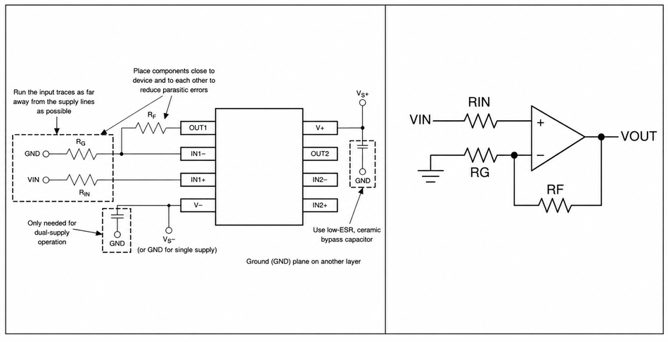
Keep resistors in the kilohm range so the amplifier operates with currents in the milliampere range and does not draw excessive current.
Check the gain bandwidth product before you commit. At 0.7 MHz GBW, a gain of 100 leaves only 7 kHz of bandwidth, and a gain of 10 leaves 70 kHz.
Inverting Amplifier
Unlike the non-inverting case, the inverting configuration needs a VQ mid-rail reference on a single supply. Gain is −RF/RI. 1
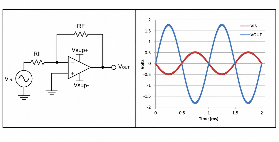
TI's design guidance recommends keeping resistors in the kilohm range so the amplifier operates with currents in the milliampere range and does not draw excessive current. TI's own worked design example uses 10 kΩ for RI and 36 kΩ for RF to yield a gain of 3.6. 1
Recommended Reading: Inverting vs Non-Inverting Op Amp: Complete Design Guide & Best Practices 2025
Using the LM358 as a Comparator
The LM358 works as a threshold detector without a VQ reference, which makes it convenient for level detection in signal conditioning circuits. A variable resistor on the non-inverting input sets the trip point.
Four cautions apply. The device is an op amp, not a dedicated comparator, so it has no internal hysteresis and no defined propagation delay. The 0.3 V/µs slew rate means the output takes about 12 µs to traverse a 3.5 V span.
Second, the output will not reach the positive rail. On a 5 V supply into 2 kΩ, the high level stops near 3.5 V, which is fine for TTL inputs at 2.0 V but marginal against a 3.5 V CMOS threshold.
Third, add positive feedback from the output to the non-inverting input to create hysteresis; otherwise, a slowly changing input will cause the output to chatter around the threshold.
Fourth, keep at least one input inside the common-mode range. Comparator circuits often drive inputs to the rails, which is exactly the condition where output phase becomes undefined.
Active Filters and Signal Conditioning
Active filters built on the LM358 need a VQ reference on a single supply, and they need bandwidth headroom. A Sallen-Key low-pass stage with a gain of 10 and a 10 kHz corner needs 100 kHz of gain bandwidth, comfortably inside the 0.7 MHz available but not with much room to spare. That headroom matters more here than in a simple gain stage: as the op-amp's own rolloff approaches its GBW limit, it adds phase shift that can shift the filter's intended corner frequency and Q, so treat 100 kHz into 700 kHz as workable rather than generous.
For transducer amplifiers, the ability to sense at ground is the reason to choose this part. A low-side current shunt or a thermocouple cold-junction circuit sits near 0 V, and the common-mode input voltage range includes the negative rail.
Recommended Reading: Instrumentation Amplifier: Theory, Three-Op-Amp Design, CMRR
DC gain blocks in voltage regulators and motor control feedback loops are the other common use. The second amplifier in the package often serves as a buffer or as the error amplifier in the same loop.
What the LM358 Is Not Good For
The LM358 is not suitable as an audio amplifier in any critical position. The independent measurements recommend it only for buffer stages or modest gain of 6 dB or less in non-critical, line-level areas, and specifically not for low-impedance loads with outputs above 1 V. For any critical audio path, dedicated low-distortion op-amps such as the NE5532 or OPA2134 remain the better choice.
Capacitive load drive is limited to about 100 pF on the B version. Driving long cables or the input of a sampling ADC without an isolation resistor risks instability.
LM358 vs LM324 vs LM741
These three parts cover the same jelly-bean territory, so the comparison comes up constantly.
Parameter | LM358 | LM324 | LM741C |
Amplifiers per package | 2 | 4 | 1 |
Pin count | 8 | 14 | 8 |
Supply range | 3 V to 30 V, single or split | 3 V to 30V recommended,32 V absolute maximum; single or split. 3 | ±10 V to ±18 V recommended. 4 |
Common-mode range includes ground | Yes, V- to V+ minus 1.5 V | Yes, 0 V to VCC minus 1.5 V | No, ±12 V min at ±15 V supply |
Input offset voltage, 25 °C | 3 mV typ, 7 mV max | 3 mV typ, 7 mV max | 2 mV typ, 6 mV max |
Input bias current, 25 °C | -20 nA typ, -250 nA max | -20 nA typ, -250 nA max | 80 nA typ, 500 nA max |
Supply current | 350 µA typ per amplifier | 0.7 mA typ for all four | 1.7 mA typ, 2.8 mA max |
Operating temperature | 0 °C to 70 °C | 0 °C to 70 °C | 0 °C to 70 °C. |
Offset null pins | No | No | Yes, pins 1 and 5 |
Sources: Texas Instruments LM358,¹ LM324,³ and LM741⁴ datasheets.
The decision is usually simple. Choose the LM324 when you need four channels in one package and board area allows a 14-pin footprint. Choose the LM358 when two channels are enough, and you want the smaller 8-pin outline. Given how many second-source manufacturers make pin-compatible versions of both parts, it's worth checking current stock and pricing across vendors before committing to a specific part number. FindChips tracks distributor listings for LM358, LM324, and LM741.
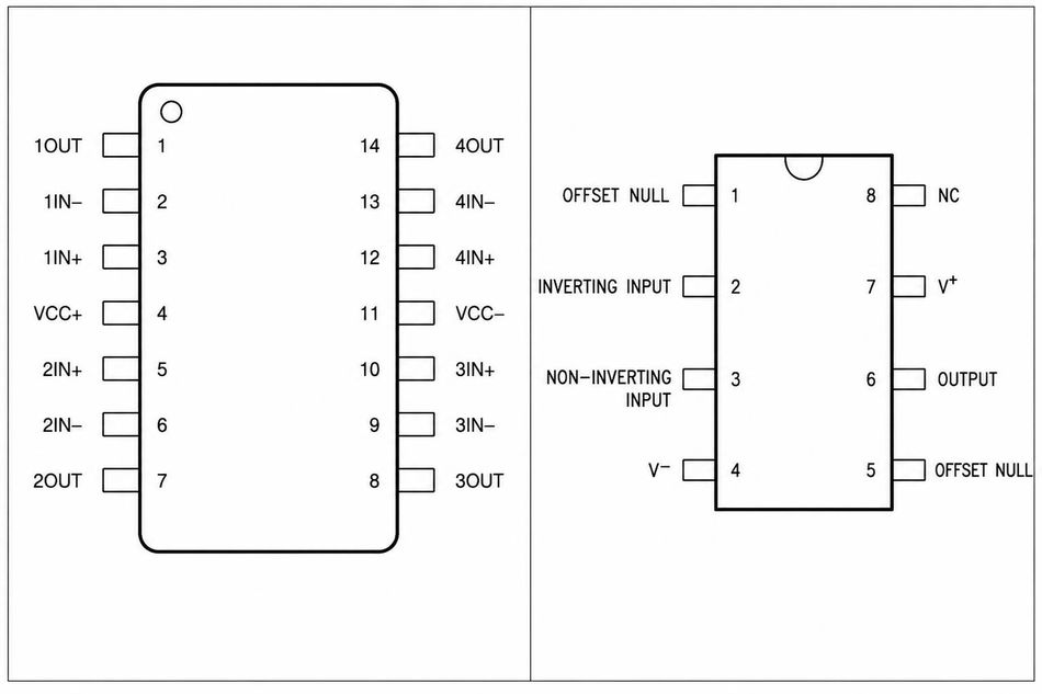
The LM741 is the one to avoid in new single-supply designs. It cannot sense to ground; it draws 1.7 mA for a single amplifier against 350 µA per amplifier for the LM358 in single-supply operation. While technically possible with careful biasing, it sacrifices most of its usable headroom.
Design Considerations and Common Mistakes
Follow the decoupling guidance from the datasheet, along with standard PCB layout practice:
Place a low-ESR 0.1 µF ceramic bypass capacitor between each supply pin and ground, as close to the device as possible. A single capacitor from V+ to ground is sufficient for single-supply circuits. Without local decoupling, noise couples into the analog circuitry through the supply pins.
Separate analog and digital grounds, and use a ground plane on a separate layer to distribute heat and reduce EMI pickup.
Route input traces as far from supply and output traces as possible. Where they must cross, cross at right angles rather than running parallel.
Keep input traces short and place feedback components close to the inverting input to minimise parasitic capacitance.
Consider a driven guard ring around high-impedance input traces to reduce leakage from nearby nodes at different potentials.
The recurring mistakes in LM358 designs are predictable. Expecting rail-to-rail output is the most common, followed by ignoring crossover distortion on split supplies, exceeding the common-mode range at the top end, and specifying the commercial 0 °C to 70 °C grade for equipment that will see sub-zero temperatures.
At 350 µA of quiescent current per amplifier, self-heating is negligible, but the PDIP-8 package has a junction-to-ambient thermal resistance of 80.9 °C/W against 124.7 °C/W for SOIC-8. If you are sourcing 20 mA continuously into a load, check the junction temperature against the 125°C maximum.
Conclusion
The LM358 remains a sound default for single-supply DC and low-frequency signal conditioning, and its ground-sensing input range is still the reason to reach for it. Its limits are well documented and easy to design around once you know them.
Budget your headroom at 1.5 V to 4 V short of VCC at the top of the swing, depending on load and supply voltage. Add a pull-down resistor whenever the load is not returned to the negative rail, and keep the required gain bandwidth well inside 0.7 MHz. For new designs, specify the LM358B and take the wider supply range, higher bandwidth, lower offset, and 2 kV ESD rating at no cost in quiescent current.
Frequently Asked Questions
What is the LM358?
The LM358 is a dual operational amplifier IC; two independent op amps in a single 8-pin package. It runs on a single supply from 3 V to 30 V (or split supplies) and, unlike older op-amps, both its input and output work down to ground. National Semiconductor introduced it in 1976; TI has made it since 2011.
What is the LM358 used for?
The LM358 is used for transducer amplifiers, DC gain blocks, and conventional op amp circuits in single-supply systems. TI lists motor control, power supplies and mobile chargers, uninterruptible power supplies, multi-function printers, and home appliances among its target applications. It also serves as the error amplifier inside linear voltage regulators. 1
Can the LM358 run from 5 V?
Yes. The recommended supply range starts at 3 V, and the part was designed to operate directly from the standard 5 V rail in digital systems. Remember that the output stops about 1.5 V below the positive rail, so your usable output window on 5 V is roughly 0 V to 3.5 V.
What is the maximum voltage of the LM358?
The classic LM358 is rated for 3 V to 30 V of total supply, with an absolute maximum of 32 V or ±16 V. The LM358B extends the recommended range to 36 V.
Is the LM358 rail-to-rail?
No. The LM358 input common-mode range includes the negative supply rail, but the output cannot swing to the positive rail. On a 5 V supply, the output typically reaches ground but remains about 1.5 V below the positive rail with a 2 kΩ load.
Why does my LM358 circuit distort near zero volts?
The output stage has no class AB bias, so it can exhibit crossover distortion when the output operates near ground. Add a pull-down resistor from the output to the negative supply so one output transistor stays in class A. Elliott Sound Products' bench measurements show this drops distortion from about 0.31 percent to below 0.01 percent under their test conditions.
What is the difference between the LM358 and the LM358B?
The LM358B is the next-generation version: 3 V to 36 V supply, 1.2 MHz unity-gain bandwidth against 0.7 MHz, 0.3 mV typical offset against 3 mV, 300 µA quiescent current per amplifier against 350 µA, 2 kV HBM ESD rating against 500 V, and an integrated RF and EMI filter.
Can I use the LM358 as a comparator?
It works as a threshold detector, but it is an op amp with no internal hysteresis and a 0.3 V/µs slew rate. Add positive feedback for hysteresis, and use a dedicated comparator such as the LM393 where speed or clean logic levels matter.
How much current can an LM358 output drive?
It sources 20 mA minimum and 30 mA typical, and sinks 10 mA minimum and 20 mA typical, at a 15 V supply. Short-circuit current is ±40 mA typical.
What does the suffix on an LM358 part number mean?
It identifies the package. LM358P is PDIP-8, LM358D is SOIC-8, LM358PW is TSSOP-8, and LM358DGK is VSSOP-8. LM358N is the PDIP suffix used by several second-source vendors.
What can replace an LM358?
For a drop-in upgrade, the LM358B keeps the pinout and improves most key electrical parameters. If you need four channels, the LM324 shares the same architecture in a 14-pin package. For audio or precision work, move to a purpose-designed part rather than trying to fix the LM358.
References
Texas Instruments, "LM158, LM258, LM358, LM2904 industry-standard dual operational amplifiers," SLOS068AB, Oct. 2024. [Online]. Available: https://www.ti.com/lit/ds/symlink/lm358.pdf
Texas Instruments, "AN-116: Use the LM158/LM258/LM358 dual, single supply op amp," SNOA662B, Apr. 2013. [Online]. Available: https://www.ti.com/lit/an/snoa662b/snoa662b.pdf
Texas Instruments, "LMx24, LM2902 quadruple operational amplifiers," SLOS066AE, Sep. 2025. [Online]. Available: https://www.ti.com/lit/ds/symlink/lm324.pdf
Texas Instruments, "LM741 operational amplifier," SNOSC25D, Oct. 2015. [Online]. Available: https://www.ti.com/lit/ds/symlink/lm741.pdf
R. Elliott, "LM358 for audio," Elliott Sound Products. [Online]. Available: https://sound-au.com/articles/lm358.htm
in this article
1. Key Takeaways2. Introduction3. What Is the LM358 IC?4. The LM358 Family: LM158, LM258, LM29045. LM358 Pinout and Pin Configuration6. Package Options and Part Number Suffixes7. LM358 Datasheet Specifications 8. How Single-Supply Operation Works9. The Output Stage: Crossover Distortion and the Fix10. LM358 Circuit Examples11. LM358 vs LM324 vs LM74112. Design Considerations and Common Mistakes13. Conclusion14. Frequently Asked Questions15. References