FPGA Chip: Architecture, Fabrication, and Families
Field-programmable gate arrays are reconfigurable integrated circuits engineered for parallel hardware acceleration. Learn how FPGA architecture works, how they're fabricated, and which FPGA chip families lead the industry.

29 May, 2026. 18 minutes read
Key Takeaways
Reconfigurable hardware fabric: An FPGA chip contains a two-dimensional array of configurable logic blocks (CLBs) with lookup tables, flip-flops, and multiplexers, surrounded by programmable I/O blocks and connected by a complex network of programmable interconnects [1]. The fabric lets engineers map custom digital circuits and change them at any time by loading a new bitstream.
Integrated memory and signal-processing resources: Modern FPGA chips integrate block RAM, DSP slices, transceivers, and hard IP blocks. AMD/Xilinx UltraScale+ devices additionally include UltraRAM, a high-density on-chip memory block not found across all FPGA families. These on-chip resources enable high-speed signal processing, embedded processors and memory-centric workloads [1]. Vendors such as AMD/Xilinx, Intel, and Lattice differentiate families based on the mix of resources.
Semiconductor technology matters: FPGA chips span process nodes from 28 nm to 7 nm and increasingly use FinFET transistors. Smaller nodes improve speed and enable more energy-efficient operation but increase development cost. Examples include the 28 nm Xilinx 7-series devices, Intel's 10 nm SuperFin Agilex FPGAs, and Lattice's 16 nm FinFET Nexus 2 platform — an upgrade from the original Nexus platform, which used Samsung's 28 nm FD-SOI process [3].
Multiple vendors and families: AMD/Xilinx, Intel/Altera, Lattice, Microchip, Efinix, and GOWIN offer families targeting everything from low-power edge devices to high-performance data-center accelerators. Each family combines different logic densities, memory sizes, DSP counts, and transceiver speeds [2][9].
Programming flow drives usability: Engineers describe hardware with hardware description languages (VHDL, Verilog) or high-level synthesis tools. Toolchains synthesize code into logic primitives, place and route them, then generate a bitstream to configure the chip. Simulations verify functionality before loading the bitstream into the device.
Future trends: Heterogeneous adaptive compute platforms such as Intel Versal ACAP, embedded FPGA IP (eFPGA), chiplet integration, and artificial intelligence accelerators are shaping the next generation of FPGA chips [4][6].
Introduction
FPGAs are programmable integrated circuits that allow digital designers to implement custom logic functions directly in silicon. Unlike microcontrollers, microprocessors or CPUs, which execute software on fixed hardware, or ASICs, which embed a fixed hardware design during fabrication, FPGAs combine arrays of configurable logic elements with programmable interconnects to form reconfigurable hardware. Because FPGAs can be reprogrammed after deployment by loading a new bitstream, they also serve as the primary platform for validating and prototyping ASIC designs before committing to fabrication. This capability makes FPGAs attractive in industries ranging from telecommunications and aerospace to automotive, defense, and data-center acceleration. The term FPGA chip often conflates the broad technology with the physical chip architecture and manufacturing processes.
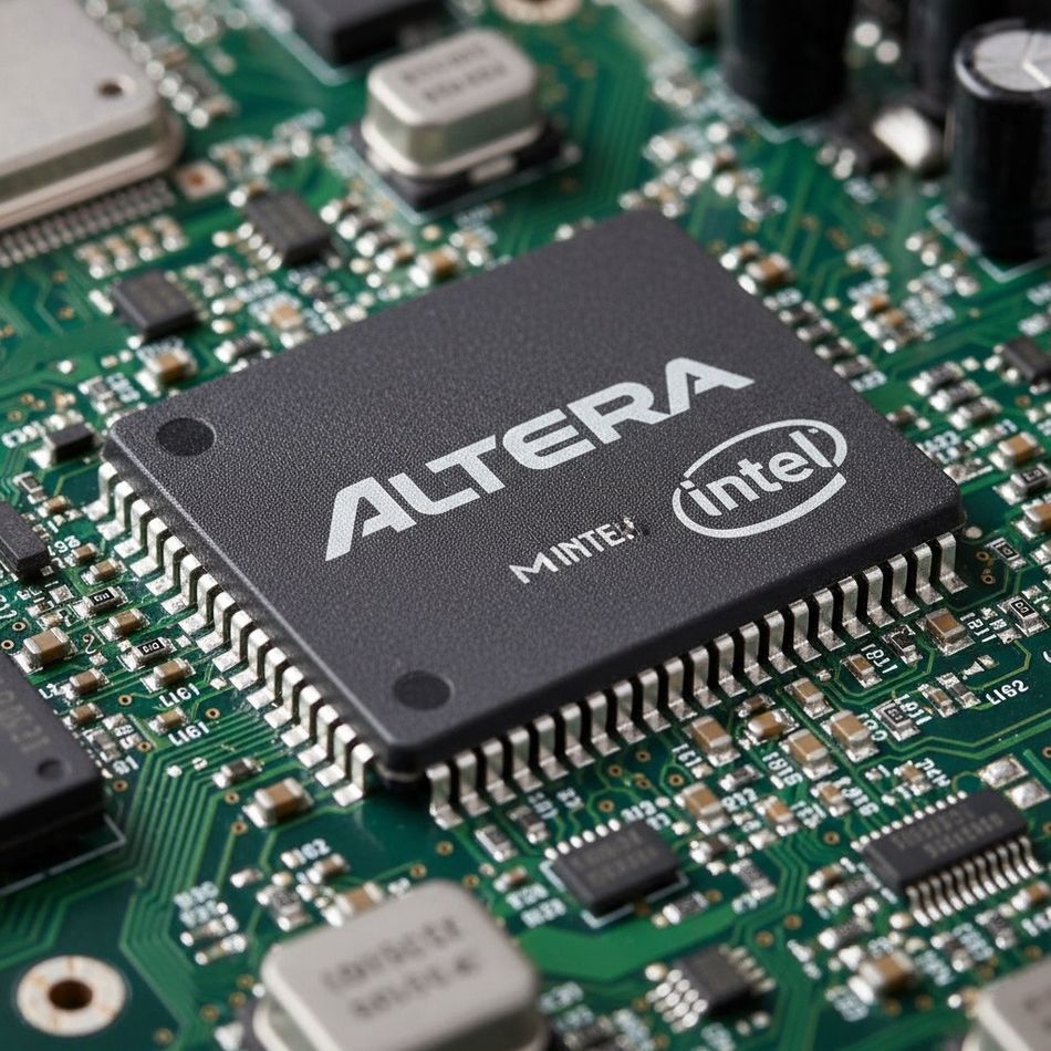
This article dissects the FPGA chip itself: its architecture, how it is fabricated, representative product families, and the emerging trends shaping its future. The discussion is intended for digital design engineers, hardware engineers, and embedded systems developers seeking tutorial and technical reference on FPGAs.
What Is an FPGA Chip?
An FPGA chip is a field-programmable gate array packaged as a semiconductor device. It contains hundreds of thousands to millions of programmable logic resources that can be wired together to implement arbitrary digital circuits. At its core, an FPGA is a reconfigurable integrated circuit composed of thousands of logic gates: the logic and interconnect configuration is stored in on-chip memory (SRAM, flash, or antifuse read-only memory), and loading a bitstream into this memory defines the function of the chip. The three main configuration memory technologies are SRAM, flash, and antifuse. In contrast, an application-specific integrated circuit (ASIC) is fabricated with a fixed logic configuration; once manufactured, its function cannot change. A microcontroller combines a CPU core, memory, and peripherals, but runs software sequentially and cannot reconfigure its logic fabric. Central processing units (CPUs) are optimized for sequential instruction execution, while graphics processing units (GPUs) contain many parallel arithmetic cores and high memory bandwidth for data-parallel workloads such as graphics rendering and AI training. FPGAs occupy a middle ground: they implement parallel hardware tailored to a specific application, such as industrial automation, like an ASIC, but remain reprogrammable for new functions.
FPGAs outperform general-purpose processors when deterministic, low-latency, or high-throughput processing is required in high-performance computing environments. Because logic pipelines execute concurrently in hardware rather than sequentially through an instruction pipeline, FPGAs can deliver higher performance per watt than CPUs or GPUs for workloads such as signal processing, network packet inspection, and real-time inference. They allow designers to build pipelines of logic that operate concurrently, delivering higher performance per watt than CPUs or GPUs for certain workloads [7]. ASICs still provide the highest performance and lowest unit cost at volume, since their fixed design eliminates the overhead of programmable routing. At the same time, CPUs and GPUs remain far easier to program in software. An FPGA chip provides a flexible and cost-effective compromise between the specialization of an ASIC and the programmability of a processor.
Inside the FPGA Chip: Architecture
Configurable Logic Fabric
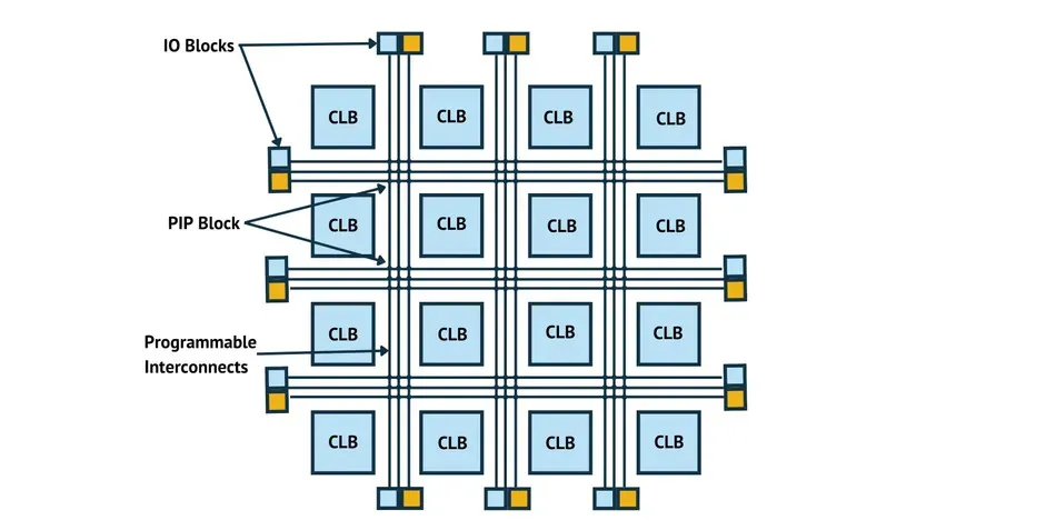
At the heart of every FPGA chip lies a two-dimensional array of configurable logic blocks (CLBs), arranged in a grid and surrounded by input/output (I/O) blocks. Each CLB contains multiple slices composed of lookup tables (LUTs), flip-flops and multiplexers. In Xilinx devices each CLB contains two slices; a SLICEL houses four six-input LUTs and eight flip-flops, with four of those storage elements configurable as either edge-triggered D-type flip-flops or level-sensitive latches. , while a SLICEM can also implement distributed RAM or shift registers [1]. LUTs implement combinational logic by storing the truth table of a Boolean function, and flip-flops provide synchronous storage for sequential logic. Carry-chain hardware accelerates arithmetic operations. Intel FPGAs use adaptive logic modules (ALMs) rather than slices; each ALM includes an 8-input fracturable LUT, two dedicated embedded adders, multiplexers, and four dedicated registers, enabling combinational or registered logic operations [1].
FPGA Architecture
Programmable Interconnects
The logic blocks within an FPGA cannot operate alone; they require a programmable interconnect network to carry signals between resources. Modern FPGAs devote most of the silicon area to routing: the routing network can occupy 80 to 90 percent of the chip [1]. In the island-style architecture used by Xilinx and Intel, CLBs sit at the intersections of horizontal and vertical routing channels. Local routing wires connect logic within a CLB, short interconnects span nearby CLBs, and long or global lines traverse multiple rows or columns [1]. Programmable switch matrices and connection boxes allow arbitrary connections between wires and CLB pins [1]. Each switch is controlled by configuration memory, typically implemented in SRAM; activating specific switches defines the wiring pattern across the chip [1].
Recommended Reading: FPGA Programming: Theory, Workflow, and Practical Implementations
Memory Blocks
While LUTs can implement small memories, FPGAs include dedicated block RAM (BRAM) and, in higher-end devices, UltraRAM. BRAM typically comes in kilobit-sized blocks with dual-port read/write capability, enabling efficient implementation of FIFOs, caches, and buffers. UltraRAM provides larger, denser memory with higher throughput for workloads such as video buffering and weight storage. I/O blocks also contain DDR flip-flops that support double-data-rate (DDR) interfaces. Many FPGAs integrate distributed RAM within slices (SLICEM) or support turning LUTs into small RAMs [1].
DSP Slices and Arithmetic Blocks
Digital signal processing requires multiply-accumulate and fixed-point arithmetic, which is inefficient to implement solely with LUTs. Modern FPGA chips provide dedicated DSP slices that include multipliers, accumulators, pre-adders and barrel shifters. These slices deliver high-performance arithmetic for FIR filters, FFTs and neural network operations. Some families augment DSP slices with hard floating-point units or AI engines to accelerate machine-learning workloads.
High-Speed Transceivers and I/O Blocks
Surrounding the logic fabric are input/output blocks (IOBs) that provide the electrical interface to the outside world. IOBs contain programmable input and output buffers, level shifters and termination resistors, supporting various single-ended and differential signaling standards including LVCMOS, LVTTL, LVDS and SSTL [1]. Many FPGAs integrate high-speed serial transceivers that implement protocols like PCI Express, Ethernet, Serial RapidIO and JESD204; these transceivers operate at multi-gigabit rates and include clock-recovery circuitry to maintain signal integrity [1]. Newer devices also embed integrated PCIe Gen4/Gen5 controllers, MIPI D/C-PHY and advanced SERDES as seen in Lattice's Nexus 2 platform [3].
On-Chip Processors and Hard IP
High-end FPGA chips often embed hardened processors and peripheral controllers. AMD/Xilinx Zynq UltraScale+ devices integrate quad-core ARM Cortex-A53 application processors and dual-core Cortex-R5 real-time processors. Versal ACAP devices replace the A53 with a dual-core ARM Cortex-A72 and retain the dual-core Cortex-R5F. . Hard IP blocks such as DDR controllers, high-bandwidth memory (HBM), Ethernet MACs, PCIe controllers, ADCs and DSP cores reduce the need to implement these functions in the programmable fabric, saving resources and power.
How FPGA Chips Are Made
Semiconductor Process Nodes and Transistors
The performance, power efficiency and cost of an FPGA chip depend heavily on the underlying semiconductor technology. Early FPGAs were built using planar CMOS processes with feature sizes exceeding 150 nm; modern devices employ FinFET transistors at 28 nm, 16 nm, 10 nm and 7 nm nodes. FinFETs reduce leakage current and improve drive strength by wrapping the gate around a fin-shaped channel, enabling smaller devices and higher frequencies. AMD/Xilinx's 7-series FPGAs are fabricated on a 28 nm high-k metal gate (HKMG) process [2]. Intel's Cyclone V FPGAs also use a 28 nm node with up to 301K logic elements [9]. Lattice's first-generation Nexus platform is based on a 28 nm fully depleted silicon-on-insulator (FD-SOI) process, while its second-generation Nexus 2 platform migrates to a 16 nm FinFET process with lower power and higher speed [3].
High-end FPGAs push to even smaller nodes. AMD/Xilinx's Versal ACAP uses TSMC's 7 nm FinFET technology [4]. Intel's Agilex FPGAs are built on the company's 10 nm process and employ 3D heterogeneous system-in-package technology to bond FPGAs, HBM and transceivers on separate tiles [8]. Such advanced nodes enable multi-GHz transceivers and high logic densities but require sophisticated design rules and yield management.
Fabrication Flow
Manufacturing an FPGA chip follows the same basic steps as other integrated circuits: wafer fabrication, assembly and test. The foundry begins with a pure silicon wafer and performs photolithography, ion implantation, deposition and etching steps to define transistors and interconnect layers. FPGAs may require additional steps for non-volatile configuration memory (flash or antifuse) or for embedding resistive random-access memory (ReRAM) used in some eFPGA cores. After wafer processing, diced dies are packaged using flip-chip ball-grid arrays (BGAs), fine-pitch chip-scale packages or multi-chip modules. Advanced packaging techniques such as embedded multi-die interconnect bridge (EMIB) and 3D stacking enable chiplet-based FPGAs by integrating logic, transceivers and memory on separate dies.
Major FPGA Manufacturers and Process Technologies
AMD/Xilinx offers families from low-cost Spartan-7 to high-end Versal adaptive SoCs. The 7-series is fabricated on a 28 nm HKMG process and includes up to 2 million logic cells, abundant BRAM, and multi-gigabit transceivers [2]. UltraScale families use 20 nm planar transistors, while UltraScale+ and Versal families adopt 16 nm and 7 nm FinFETs, respectively.
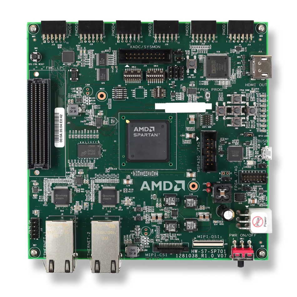
The SP701 Evaluation Kit with AMD Spartan™ 7 FPGA. Source: AMD
Intel (formerly Altera) offers Cyclone V (28 nm, up to 301K logic elements, 6 Mb RAM, and 112 DSP blocks [9]), Arria 10 (20 nm with hardened floating-point units), Stratix 10 GX (14 nm, 10.2 M logic elements with 96 transceivers [10]), and Agilex (10 nm, heterogeneous chiplet architecture). Agilex provides 40 percent higher performance or 40 percent lower power than Stratix 10, supports BFLOAT16 arithmetic, and features transceiver speeds up to 112 Gbps [8].
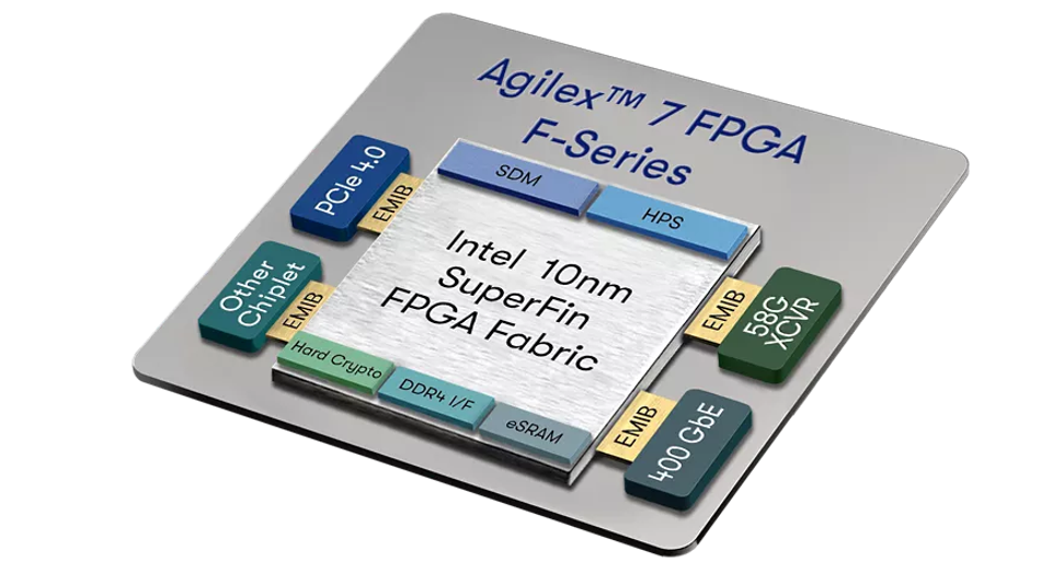
Agilex 7 FPGA F-Series. Source: Altera
Lattice Semiconductor focuses on low-power, cost-optimized devices. The iCE40 family uses a 40 nm process and offers 384 to 7,680 LUT4s and as few as 21 µA standby current [3]. The ECP5 family provides up to 85 k LUTs in small 10×10 mm packages and supports SERDES rates up to 3.2 Gbps (5 Gbps for the ECP5-5G) [3]. The Nexus 2 platform is built on a 16 nm FinFET process with integrated multi-protocol 16G SERDES, PCIe Gen4 controller, and MIPI D/C-PHY up to 7.98 Gbps [3].
Lattice Semiconductor MachXO5 - NXTDQ. Source: Lattice Semiconductor
Microchip PolarFire FPGAs and SoCs use a 28 nm SONOS non-volatile process with up to 480 k logic elements [11]. PolarFire SoCs combine five 64-bit RISC-V cores with FPGA fabric, delivering low-power operation and secure boot for industrial and defense applications.
Microchip PolarFire FPGA. Source: Microchip
Efinix Trion FPGAs target low-power and IoT markets. Built on a 40 nm process, they offer 4 k to 120 k logic elements and include small wafer-level packages with integrated MIPI CSI-2 and DDR controllers [12].
GOWIN Semiconductor produces flash-based FPGAs (LittleBee) with 1 k–10 k logic elements and SRAM-based devices, including Arora (20K–55K LEs) and the newer Arora V family on 22 nm with up to 138K LEs and 12.5 Gbps SERDES. These chips include on-chip memory up to 16 Mb, ADC, USB, and I3C interfaces and are available in packages as small as 1.8 × 1.8 mm [13].
FPGA Chip Families and Examples
AMD/Xilinx
Family & Part Example | Process & Key Specs | Notes |
Spartan-7 (XC7S50) | 28 nm HKMG; up to ~52 k logic cells, ~2.7 Mb BRAM [2] | Cost-optimized for low-power applications |
Artix-7 (XC7A200T) | 28 nm; up to 215 k logic cells, 13 Mb BRAM and 740 DSP slices [2] | Small form factors and low power; software-defined radio, motor control, portable instrumentation |
Kintex-7 (XC7K325T) | 28 nm; up to 326 k logic cells and 16 Mb BRAM [2] | GTX transceivers up to 12.5 Gbps |
Virtex-7 (XC7V2000T) | 28 nm; up to 1.95 M logic cells, 46 Mb BRAM, and 2160 DSP slices [2] | GTH transceivers up to 13.1 Gbps; high-end signal processing |
Kintex UltraScale+ (XCKU15P) | 16 nm FinFET; up to 1.2 M logic cells, 70 Mb UltraRAM, transceivers up to 32.75 Gbps | Hardened PCIe Gen4 controller, |
Versal ACAP (VCK190) | 7 nm FinFET; dual ARM A72/R5F, adaptable logic, AI engines [4] | Network-on-chip; AI/ML, 5G, and aerospace |
Intel/Altera
Family & Part Example | Process & Key Specs | Notes |
Cyclone V (5CSEA6) | 28 nm; 110 k LEs, 6 PLLs, 6.191 Mb memory, 112 DSP blocks [9] | Low-cost family with balanced logic/memory resources |
Arria 10 (10AX115U) | 20 nm; up to 1.150 K LEs, hardened floating-point DSP, high-bandwidth transceivers | Mid-range communications and video processing |
Stratix 10 GX (GX 10M) ) | Intel 14 nm with EMIB packaging; 10.2 M LEs, 48 transceivers, 308 Mb memory [10] | HyperFlex architecture; dual EMIB-bonded FPGA dies for ASIC prototyping and emulation |
Agilex 7 (AGM032) | Intel 7 FinFET with 3D heterogeneous SiP; 3.24 M LEs, 116 Gbps transceivers, DDR5/HBM2E | ~~50% higher performance or ~40% lower power vs Stratix 10; BFLOAT16 and FP16 hardened arithmetic for AI; PCIe Gen 5 and CXL support |
Lattice, Microchip, Efinix, GOWIN
Family & Part Example | Process & Key Specs | Notes |
Lattice iCE40 LP/HX (iCE40HX8K) | 40 nm; 384–7,680 LUT4s; standby current as low as 21 µA [3] | Ultra-low-power for wearable and mobile products |
Lattice ECP5/ECP5-5G | 40 nm; up to 85 k LUTs, SERDES to 3.2 Gbps (5 Gbps for -5G) [3] | Mid-range for small form-factor communications and industrial |
Lattice Certus-NX/Certus-N2 | 28 nm FD-SOI (NX) / 16 nm FinFET (N2); 16G SERDES, PCIe Gen4, LPDDR4 [3] | Nexus 2 provides up to 2× logic cells and >3× DSP cores vs first gen [3] |
Microchip PolarFire (MPF300T) | 28 nm SONOS; 300K LEs, up to 20.6 Mb memory, 924 math blocks [11] | Non-volatile configuration; aerospace, industrial, defense |
Microchip PolarFire SoC (MPFS460T) | 28 nm SONOS with five 64-bit RISC-V cores and 461 k LEs [11] | Combines programmable logic with a multi-core RISC-V CPU subsystem |
Efinix Trion T4–T120 | 40 nm; 4 k–120 k LEs, 77 kbits–5.4 Mbits embedded RAM [12] | MIPI CSI-2, LVDS and DDR controllers; low-power IoT and vision |
GOWIN LittleBee/Arora | Flash-based (1 k–9 k LEs) and SRAM-based (20 k–55 k LEs) [13] | Packages as small as 1.8 × 1.8 mm; integrated ADC, USB and I3C |
Programming an FPGA Chip
Designing for an FPGA chip involves several stages supported by specialized CAD tools:
Hardware description: Engineers describe desired logic functions using HDLs such as VHDL and Verilog. These languages let designers specify concurrent processes, clock domains, finite-state machines and arithmetic operations. High-level synthesis (HLS) tools translate algorithmic descriptions written in C/C++ into HDL.
Simulation: Designs are simulated at the RTL (register-transfer level) to verify functional correctness. Testbenches stimulate the design and check outputs against expected results.
Synthesis: The synthesis tool converts HDL into a netlist of logic elements (LUTs, flip-flops, memory blocks and DSP slices), performing optimizations such as resource sharing, pipelining and retiming.
Place and route: The place-and-route tool assigns synthesized primitives to physical sites and configures the programmable interconnect. Routing must satisfy timing constraints and minimize congestion [1].
Bitstream generation: The tool generates a configuration bitstream containing the values that define LUT contents, flip-flop enables, routing switch settings and I/O parameters. Loading the bitstream into the FPGA initializes the hardware.
Programming and debugging: The bitstream is programmed into the FPGA via JTAG, SPI flash or secure boot loader. On-chip logic analyzers and embedded processors facilitate debugging. Partial reconfiguration allows portions of the logic fabric to be reprogrammed without halting the rest of the system.
Toolchains differ among vendors: AMD Vivado/Vitis integrates C++, OpenCL, and Python frameworks; Intel's Quartus Prime supports VHDL, Verilog, SystemVerilog, and OpenCL; Lattice Radiant and Propel provide low-power design flows.
Recommended Reading: FPGA Programming: Theory, Workflow, and Practical Implementations
Applications of FPGA Chips
Data Center Acceleration
Hyperscale data centers deploy fpga-based cards to offload computation from CPUs. FPGAs accelerate network packet processing, storage compression, encryption, and database search by mapping algorithms directly into hardware pipelines. AMD's Versal devices integrate AI engines and network-on-chip to handle machine-learning inference with microsecond latency [4]. Intel's Agilex FPGAs support PCIe Gen5 and high-bandwidth memory; Stratix 10 supports PCIe Gen4 and HBM, enabling accelerators for cloud AI and analytics.
AI and Machine Learning
FPGAs are well-suited to inference workloads because they combine massively parallel DSP slices with reconfigurable logic. Designers implement convolutional neural networks, transformers, and graph models using quantized arithmetic and custom dataflows. Versal ACAP's AI engines (VLIW vector processors) accelerate matrix multiplication and convolution operations [4]. Lattice's low-power Nexus 2 devices target edge AI, supporting LPDDR4 and MIPI interfaces for vision tasks [3].
Recommended Reading: What are FPGAs used for? A Deep Dive Into Architecture, Advantages, and Modern Applications
Telecommunications and 5G
Wireless infrastructure demands real-time processing of high-bandwidth signals. FPGAs implement baseband functions such as digital up/down conversion, channel coding/decoding, and beamforming. High-speed transceivers support fronthaul protocols like CPRI and eCPRI, while programmable logic enables dynamic adaptation to evolving 5G standards.
Automotive and Aerospace
Modern vehicles incorporate ADAS, infotainment, and zonal architectures. FPGAs enable sensor fusion, real-time AI, radar signal processing, and secure networking within automotive temperature and reliability constraints. Lattice's Certus-NX FPGAs wake nearly instantaneously and provide up to 4× better power efficiency than competing devices [3]. In aerospace and defense, Microchip's PolarFire SoC offers non-volatile configuration and radiation-tolerant operation [11].
Signal Processing and Prototyping
FPGAs excel at digital signal processing tasks such as filtering, modulation, error correction and image processing due to their parallelism and dedicated DSP slices. They also serve as prototyping platforms for ASIC designs: engineers validate algorithms and interfaces on an FPGA before committing to a fixed ASIC. When production volumes grow, they may migrate to an ASIC or to embedded FPGA (eFPGA) IP integrated into the SoC.
FPGA Chip vs ASIC vs CPU vs GPU
Attribute | FPGA Chip | ASIC | CPU | GPU |
Architecture | Reconfigurable LUTs, flip-flops, BRAM, DSP slices with programmable interconnects [1] | Fixed logic and interconnect defined during fabrication | Von Neumann/Harvard with scalar cores, caches, branch predictors | Many-core SIMD with thousands of arithmetic units |
Design Cost & Time | Moderate. No NRE mask cost; HDL and synthesis. Fast iteration | High NRE (millions USD); months to years design cycle | Minimal HW cost; software development cost varies | GPU programming frameworks; no HW design cost |
Unit Cost | Higher than ASIC at high volume; constant per chip | Lowest at high volume | Low per CPU core; widely manufactured | Moderate; specialized memory and interconnect |
Performance per Watt | High efficiency for specific pipelines [7] | Highest when optimized for a single function | Lower due to general-purpose design and OS overhead [7] | Good for parallel workloads; poor for sequential |
Latency & Determinism | Very low latency; deterministic timing without OS overhead [7] | Lowest possible; fully custom | Higher; OS scheduling and branch prediction | Moderate; good for streaming, not control loops |
Flexibility | Reprogrammable post-deployment | None; fixed | Flexible via software | Flexible for data-parallel workloads |
Typical Applications | Real-time signal processing, hardware accelerators, prototyping, embedded control | Network switches, storage controllers, SoCs | General-purpose computing, OS applications | Graphics, AI inference/training, scientific simulation |
FPGAs provide a unique trade-off: hardware-level parallelism and low latency like ASICs while maintaining the reprogrammability of software-driven processors. Designers select FPGAs when they require deterministic performance and adaptability without ASIC NRE costs.
Recommended Reading: ASIC vs FPGA: A Comprehensive Comparison
Future Trends
Adaptive Compute and ACAPs
AMD's Versal Adaptive Compute Acceleration Platform exemplifies the convergence of CPUs, programmable logic and AI accelerators. Versal chips integrate scalar engines (ARM Cortex-A72 and Cortex-R5F), adaptable engines (programmable logic with BRAM and UltraRAM) and intelligent engines (arrays of VLIW/SIMD AI cores) [4]. A network-on-chip interconnect ties these engines to on-chip memory and I/O [4]. ACAPs will likely become mainstream in applications where flexibility and performance must coexist, such as 5G base stations, aerospace radars and edge AI devices.
Embedded FPGA (eFPGA) IP
A growing trend is the integration of embedded FPGA (eFPGA) IP directly into custom ASICs and system-on-chip designs. Unlike standalone FPGAs, eFPGA cores are delivered as IP blocks that SoC designers incorporate into their chips. Customers can achieve an 80–90% reduction in cost and power by replacing a standalone FPGA with licensed eFPGA IP while preserving design flexibility , and Analog Devices’ Flex Logix EFLX technology offers arrays from a few thousand to hundreds of thousands of LUTs across 7 nm to 40 nm nodes [6]. Modular architectures let designers distribute eFPGA tiles across the die [6]. Modern eFPGA IP uses the same 7 nm technology as high-performance standalone FPGAs and enables migration paths from FPGA prototypes to ASICs without losing programmability [5]. Customers can achieve up to 90 percent reduction in device cost by replacing a standalone FPGA with licensed eFPGA IP while preserving design flexibility [5].
Chiplet Integration and 3D Packaging
Advanced FPGAs already leverage chiplet architectures and 3D packaging. Intel's Stratix 10 and Agilex families use embedded multi-die interconnect bridge (EMIB) to join FPGA cores, transceiver tiles and high-bandwidth memory in a single package [10]. This approach improves yield and allows heterogeneous process nodes. Future FPGA chips may adopt chiplet ecosystems with standardized interconnects, enabling designers to mix and match compute, memory, analog and I/O tiles.
AI-Centric FPGAs and Domain-Specific Accelerators
AI and machine learning workloads drive innovations in FPGA architecture. Vendors are adding AI engines, tensor cores and sparse compute units directly into chips. AMD's Versal AI Core and AI Edge families integrate hundreds of AI engine tiles; Intel's Agilex includes BFLOAT16 and INT8 support and provides up to 112 Gbps transceivers [8]. Lattice is focusing on low-power edge inferencing, offering designs like Certus-N2 with up to three times more DSP cores than previous generations [3].
Open-Source Toolchains and High-Level Languages
Traditional FPGA development relies on proprietary CAD tools, but the community has made strides toward open-source alternatives. Projects like Yosys, nextpnr and Project X-ray provide synthesis and bitstream generation for certain devices, notably Lattice iCE40. Higher-level languages and frameworks such as Chisel, MyHDL and Migen allow hardware to be described in Python or Scala and compiled down to Verilog.
Conclusion
FPGA chips are remarkable feats of engineering, combining reconfigurable logic, programmable interconnects, embedded memory, and specialized processing units into a single integrated circuit. Their architecture, an array of configurable logic blocks, memory blocks, DSP slices, and high-speed I/O connected by a massive routing network, enables engineers to implement complex hardware functions and reconfigure them on demand [1]. Fabrication advances from 40 nm planar CMOS to 7 nm FinFET have increased logic density, reduced power consumption and allowed integration of hardened processors, transceivers and AI engines [3][8]. A rich ecosystem of families from AMD/Xilinx, Intel, Lattice, Microchip, Efinix and GOWIN offers solutions tailored to low-power IoT devices, mid-range industrial systems and high-performance data centers. As technologies like ACAPs, eFPGA IP, chiplet integration and AI engines mature, FPGA chips will continue to evolve into heterogeneous adaptive platforms blending software programmability, hardware efficiency and domain-specific acceleration.
FAQ
What is inside an FPGA chip?
An FPGA chip contains a grid of configurable logic blocks (CLBs) with lookup tables, flip-flops and multiplexers; programmable interconnects; embedded memory blocks; DSP slices for arithmetic; high-speed transceivers; and input/output blocks. Higher-end devices also integrate hard processors and AI engines. These elements can be reconfigured by loading a bitstream, allowing the chip to implement custom hardware functions [1].
Who makes FPGA chips?
Several semiconductor companies produce FPGA chips. AMD (which acquired Xilinx) offers Spartan-7, Artix-7, Kintex, Virtex, and Versal families fabricated on 28 nm to 7 nm processes [2]. Intel (formerly Altera) offers Cyclone V, Arria 10, Stratix 10, and Agilex families using 28 nm, 20 nm, 14 nm, and 10 nm technologies [9][10]. Lattice Semiconductor supplies iCE40, ECP5, and Nexus/Nexus-2 devices for low-power applications [3]. Other suppliers include Microchip (PolarFire and PolarFire SoC), Efinix (Trion), GOWIN (LittleBee and Arora), and Achronix (Speedster7t FPGAs and Speedcore eFPGA IP).
How much does an FPGA chip cost?
Prices vary widely depending on logic density, features and package. Small low-power devices like Lattice iCE40 or GOWIN LittleBee can cost a few euros per unit in quantity. Mid-range FPGAs such as AMD Artix-7 or Intel Cyclone V range from tens to hundreds of euros. High-end chips like AMD Virtex UltraScale+, Intel Stratix 10 or Versal ACAP can cost several thousand euros each. Development boards and evaluation kits add additional cost but provide necessary power supplies and interfaces.
FPGA chip vs microcontroller: how do they differ?
Microcontrollers integrate a general-purpose processor core, memory and peripherals on a single chip and execute instructions sequentially. They are easy to program in C or Python and ideal for control-oriented tasks. An FPGA chip contains no fixed processor by default; instead, it provides a reconfigurable logic fabric that can implement custom hardware circuits in parallel. This gives FPGAs lower latency and higher throughput for tasks like signal processing or encryption but requires hardware description languages and synthesis tools to design the logic. Many modern SoCs combine both: an embedded CPU subsystem and FPGA fabric for the best of both worlds.
How does an FPGA chip work?
An FPGA chip operates by configuring the values of internal SRAM cells (or flash/antifuse elements) that control LUT contents, flip-flop resets, routing switches and I/O settings. When a bitstream is loaded, these configuration bits program the logic blocks and interconnect to implement the desired circuit. After configuration, the FPGA behaves like custom hardware, executing operations concurrently and at hardware clock rates. Reprogramming the device simply requires loading a new bitstream.
Are FPGA chips reprogrammable?
Yes. Most commercial FPGAs use SRAM-based configuration memory that can be rewritten an unlimited number of times. Designers can reprogram the entire device or use partial reconfiguration to change portions of the logic fabric while the rest of the system remains operational. Some non-volatile FPGAs (Microchip PolarFire) use flash-based configuration; these can also be reprogrammed, but the number of cycles may be limited.
What is the most powerful FPGA chip?
As of 2026, the most powerful general-purpose FPGAs include Intel's Stratix 10 and Agilex 7 and AMD's Virtex UltraScale+ and Versal Premium families. The Stratix 10 GX provides up to 10.2 million logic elements and dozens of high-speed transceivers [10], while Agilex devices add HBM and high-speed transceivers [8]. AMD's Virtex UltraScale+ and Versal ACAPs integrate millions of logic cells, advanced DSP slices, and AI engines [4]. The definition of most powerful depends on whether logic density, transceiver bandwidth, or AI acceleration is prioritized.
References
[1] Wevolver, "FPGA Architecture: A Comprehensive Guide for Digital Design Engineers," Wevolver, [Online]. Available: Link. [Accessed: 2025].
[2] AMD, "7-Series FPGAs Data Sheet: Overview," DS180, AMD Documentation, [Online]. Available: Link. [Accessed: 2025].
[3] Lattice Semiconductor, "How Small FPGAs Can Make a Big Impact: Nexus 2 Platform," Lattice Semiconductor, [Online]. Available: Link. [Accessed: 2025].
[4] MosChip, "Versal ACAP Architecture and Intelligent Solution Design," MosChip Blog, [Online]. Available: Link. [Accessed: 2025].
[5] Achronix Semiconductor, "Benefits of Using FPGA and eFPGA IP in Your Design," Achronix Blog, [Online]. Available: Link. [Accessed: 2025].
[6] EDN, "How eFPGA IP Suppliers Are All Set to Raise the SoC Design Game," EDN, [Online]. Available: Link. [Accessed: 2025].
[7] Digilent, "Six Reasons You Should Consider FPGAs Over ASICs or CPU/GPUs," Digilent Blog, [Online]. Available: Link. [Accessed: 2025].
[8] Intel Corporation, "Intel Agilex FPGAs and SoCs," Intel, [Online]. Available: Link. [Accessed: 2025].
[9] Intel Corporation, "Cyclone V FPGAs Product Overview," Intel, [Online]. Available: Link. [Accessed: 2025].
[10] Intel Corporation, "Stratix 10 GX FPGAs Product Overview," Intel/Altera, [Online]. Available: Link. [Accessed: 2025].
[11] Microchip Technology, "PolarFire FPGA Product Brief," Microchip Technology, [Online]. Available: Link. [Accessed: 2025].
[12] Efinix, "Trion FPGA Family Datasheet," Efinix, [Online]. Available: Link. [Accessed: 2025].
[13] Alcom Electronics, "GOWIN Semiconductor FPGA Family Overview," Alcom Electronics, [Online]. Available: Link. [Accessed: 2025].
in this article
1. Key Takeaways2. Introduction3. What Is an FPGA Chip?4. Inside the FPGA Chip: Architecture5. How FPGA Chips Are Made6. FPGA Chip Families and Examples7. Programming an FPGA Chip8. Applications of FPGA Chips9. FPGA Chip vs ASIC vs CPU vs GPU10. Future Trends11. Conclusion12. FAQ13. References