D Latch: Understanding Level-Sensitive Data Latches
A reference covering D latch logic, circuit design, timing, and real-world digital applications.

04 Jun, 2026. 12 minutes read
Key Takeaways
A D latch is a level-sensitive memory element with a data input (D) and an enable or gate input (E). When the enable is asserted, the output Q follows the data input. When the enable is deasserted, the latch holds its previous output.
Because the output follows the input while the enable is asserted, a D latch is often called a transparent latch or gated D latch. When the enable goes low, the last value on D is latched and preserved.
The D latch is built from an SR latch by adding an inverter so that the S and R inputs are always complementary. This eliminates the forbidden S = R = 1 state present in the SR latch.
A D latch is a level-sensitive device. It changes state when the enable pin is high. It’s an edge-triggered fundamental element for a D flip-flop. Usually, a D flip-flop is constructed from two D latches (master and slave).
Designers must respect setup time (data must be stable before changes are enabled), hold time (data must be stable after changes are enabled), and propagation delay. Violating these times risks metastability.
Real devices such as the 74LS75 4-bit latch and 74HC373/74HC573 octal transparent latches with tri-state outputs implement D latches. When latch enable is high, Q follows D. When enable goes low, Q retains the last latched value.
Introduction
Sequential digital systems need memory elements that can hold a logic state for later use. Latches and flip-flops provide this by storing a bit and presenting it on their outputs. Combinational circuits produce outputs solely from current inputs, while sequential circuits incorporate memory to track previous events. A simple memory element is the SR latch, but it has an undefined state when both S and R inputs are asserted simultaneously.
The D latch solves this problem by reducing the SR latch's two control inputs to a single data input (D) and an enable input (E). When the enable is asserted, the latch is transparent. Q follows D. When the enable is removed, the latch holds the last output. It ignores subsequent changes on D. The D latch is an essential building block in registers, microprocessor pipelines, and memory arrays.
This article explains the behavior and truth tables, shows how the D latch is a digital circuit derived from the SR latch, compares it with the edge-triggered D flip-flop, defines timing parameters, and discusses practical hardware implementations. It concludes with applications and frequently asked questions.
What Is a D Latch
A Data latch (D latch) is a bistable memory element with two inputs:
Data input (D): carries the bit to be stored.
Enable input (E): also called gate or latch enable. Controls when the latch can change state.
When the enable input is asserted (E = 1 in an active-high design), the latch is in transparent mode. Q immediately follows D. When E goes low, the output stops following the input and retains the last value. The gate input forces S and R to levels that hold the previous state when unasserted, and to complementary levels when asserted, producing a set or reset.
In a D latch with enable high input, the D input is transferred to Q, and "the Q output will follow the data input as long as the enable remains HIGH". When enable goes low, the last data value is retained until enable is asserted again.
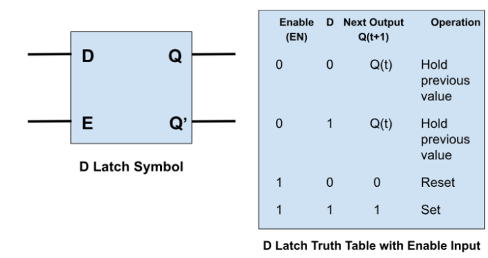
Because the output follows the input during the enable period, the D latch is often called a transparent latch. This level-sensitive behavior distinguishes it from edge-triggered devices. The latch can be active-high (enabled when E = 1) or active-low (enabled when E = 0).
D Latch Truth Table and Characteristic Table
The D latch circuit can be summarized with a truth table. The following table shows the relationship between E, D, and Qn+1.
E | D | Qn+1 | Operation |
0 | X | Qn | Hold (latched) |
1 | 0 | 0 | Reset |
1 | 1 | 1 | Set |
'X' denotes a don't-care value of the data input when enable is low. Qn+1 depends on the previous output Qn in the hold case.
The characteristic equation can also express the behavior:
Qn+1= E·D + E'·Qn
If the enable is high, the output equals the data input. If the enable is low, the output remains unchanged.
From SR Latch to D Latch
The SR latch is the fundamental bistable element made from two cross-coupled logic gates. In a NOR-based SR latch, two NOR gates feed each other. Inputs S (set) and R (reset) drive the latch.
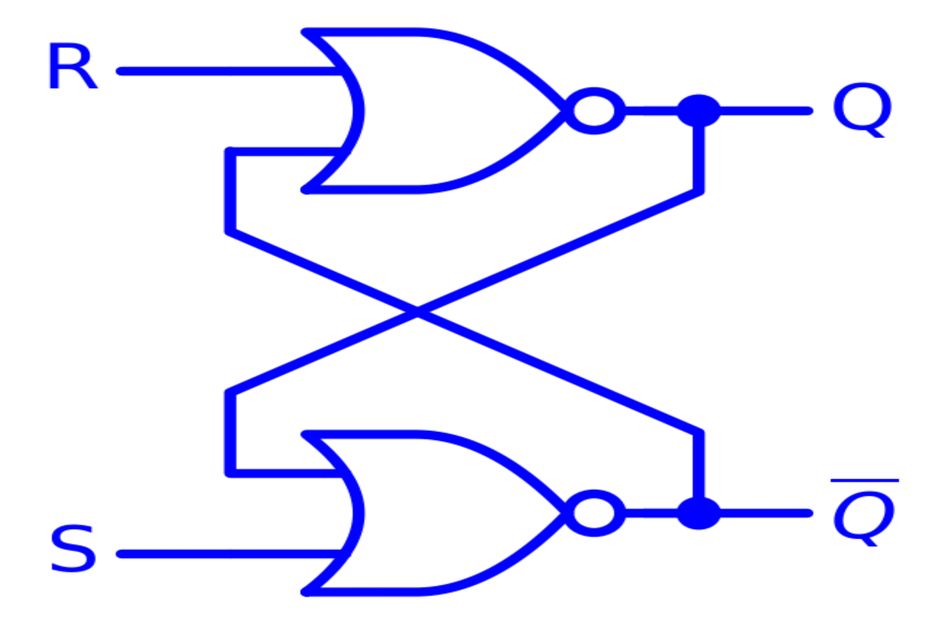
When S = 1 and R = 0, Q = 1. When S = 0 and R = 1, Q = 0. When both are 0, the latch holds. When both are 1, both outputs are driven to the same logic level, violating the complementary nature of Q and Q', creating an undefined state.
Eliminating the Forbidden State
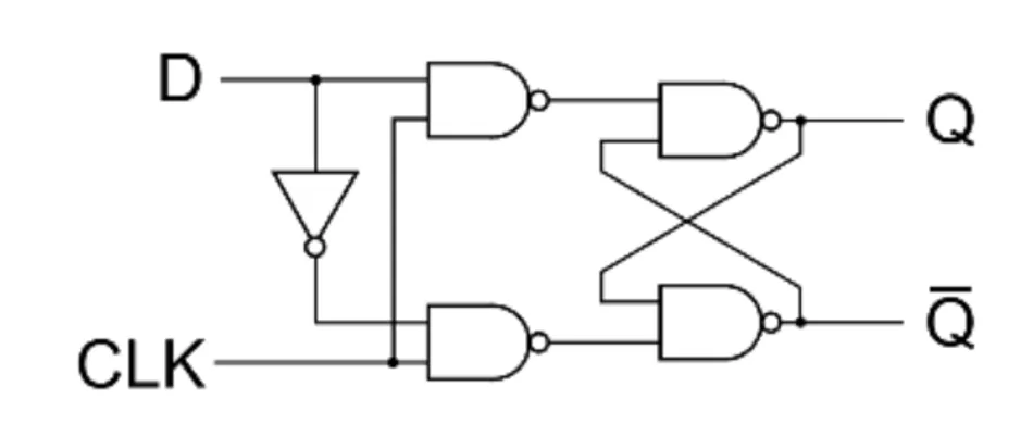
A D latch eliminates the undefined SR latch state by ensuring that S and R are never high simultaneously. This is done by placing an inverter between input D and one of the SR inputs.
In a NAND-based SR latch (active-low S and R), feeding D to one gate and D' to the other guarantees the invalid condition S = R = 0 cannot occur. When the enable gate is high, the complementary signals drive the SR latch, and it becomes transparent. When the enable is low, the outputs are forced to hold their state.
Suggested Reading: Understanding the SR Latch: Theory, Design, Truth Tables and Practical Implementations
NAND and NOR Implementations
There are two common ways to implement a D latch:
NAND-based D latch: Two NAND gates form the basic SR latch. D passes through an inverter to generate D'. Two more NAND gates combine D and D' with the enable signal. When enable is high, the latch operates normally. When enable is low, both control inputs to the SR latch are driven high, forcing it to hold.
NOR-based D latch: Two NOR gates form the SR latch with active-high S and R. D drives S directly and R through an inverter. Two AND gates controlled by the enable signal apply D and D' when enable is high. When enable is low, both inputs to the NOR latch are forced low, holding the state.
The important feature is that S and R are always complements of each other, enabling the input gates to feed data into the latch.
Recommended Reading: The Designers Guide to Logic and Its Applications
D Latch vs D Flip-Flop
Latch and flip-flop are sometimes used interchangeably, but the two devices have different timing behavior.
A D latch is level-sensitive. It responds to the enable signal level. When enable is high, Q follows D. When enable is low, Q holds its value. A latch can change its output at any time while it is enabled.
A D flip-flop is edge-triggered. It responds only to a clock (CLK) signal transition—the output updates on a specific clock edge (rising or falling).
Master-Slave Construction
A common way to implement an edge-triggered D flip-flop is to cascade two D latches in a master-slave configuration. In a positive-edge-triggered D flip-flop, the master latch is enabled when the clock is low, and the slave latch is enabled when the clock is high.
During the first half of the clock cycle, the master captures the input.
During the second half, the slave transfers the captured data to the output.
The flip-flop updates its output only on the rising edge of the clock.
Comparison Table
Device | Sensitivity | Construction | When Q follows D | Memory action |
D latch | Level-sensitive (enable) | One SR latch plus gating logic | While enable is asserted | Hold the last value when enabling the deassertion |
D flip-flop | Edge-triggered (clock) | Two latches in a master-slave configuration | On a clock edge | Holds the last value until the next clock edge |
SR latch | Level-sensitive | Two cross-coupled gates | Controlled by S and R inputs | Holds the last value when both inputs are inactive |
A D flip-flop is built from latches but behaves differently because it is edge-triggered. This is critical in timing-sensitive designs because flip-flops provide better control by sampling inputs only at discrete times.
Suggested Reading: Mastering Flip-Flop Circuits: Theory, Design, Types, and Real-World Applications
Timing Considerations
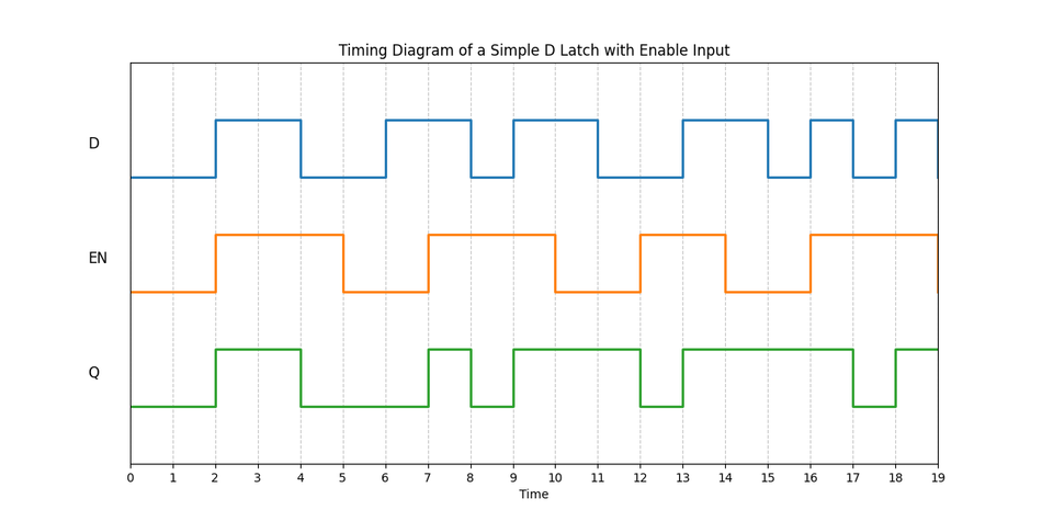
Timing Diagram
While the enable signal is high, changes on D appear on Q with a small propagation delay. When the enable goes low, Q remains fixed at its last value. The D latch samples data at specific times determined by the enable signal and holds it when disabled, which makes it the basis for shift registers and delay elements.
Propagation Delay
Propagation delay (tpd) is the time required for a change at the input to appear at the output. For a latch, tpd is the time from when D changes (with enable high) until Q reflects the new value.
Propagation delay depends on internal gate delays and load capacitance. Integrated circuit datasheets typically specify delays for both low-to-high and high-to-low transitions.
Setup Time
Setup time tsu is the minimum interval before the enable signal changes during which the data input must remain stable. If D changes too close to the falling edge of enable, the latch may not reliably capture the correct value.
Setup time is also defined as the amount of time required for the input to be stable before a clock or enable edge.
Hold Time
Hold time th is the minimum interval after the enable signal changes during which the data input must remain stable. If the data changes immediately after enable goes low, the latch may capture an incorrect value.
Metastability
Violating setup or hold times can cause a latch to enter a metastable state, where the output temporarily oscillates or remains at an indeterminate voltage before settling. When both inputs change simultaneously, the feedback loop can become unstable. This situation is best avoided to ensure that data is stable around enable transitions.
Hardware Implementations
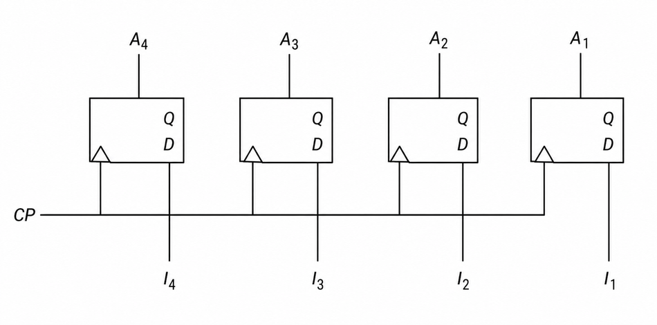
74LS75: Four-Bit D Latch
The SN54/74LS75 is a TTL integrated circuit containing four independent D latches. The Texas Instruments datasheet specifies that information present at a data (D) input is transferred to the Q output when the enable is HIGH.
The Q output follows D as long as enable remains high. When enable goes low, the data present at the transition is retained until enable returns high. The LS75 does not include tri-state outputs. Its outputs always present the stored data.
74HC373: Octal Transparent Latch
The 74HC373 and its variants (74HCT373, 74LS373) are octal (8-bit) D-type transparent latches with 3-state outputs. Each latch has an independent D input and shares a latch enable (LE) and an output enable (OE). When OE is low, the contents of the eight latches appear on the Q outputs.
When OE is high, the outputs enter a high-impedance state, allowing bus sharing. When LE is high, Dn is latched, and the output tracks the input. When LE goes low, the input data is locked, and changes in D no longer affect Q.
74HC573: Octal Latch with Tri-State Outputs
The 74HC573/74HCT573 is similar to the 74HC373 but has slightly different pinouts and timing characteristics. It is an octal D-type transparent latch with 3-state outputs. Separate D inputs, a common latch enable, and an output enable are provided. When LE is HIGH, data from the D inputs is latched.
When LE is LOW, the latches store the information present on the D inputs immediately before the high-to-low transition. The output enable controls whether the stored data appears on the outputs or whether the outputs are high-impedance. Its tri-state capability makes it ideal for bus-oriented applications.
CMOS Transmission-Gate Latch
In CMOS technology, a common implementation uses transmission gates instead of NAND/NOR gates. A transmission gate is a bidirectional switch composed of a parallel NMOS and PMOS transistor. When the gate control signal is high, both transistors conduct, and the switch connects the input to the output. When the control signal is low, both transistors are off and the path is open.
A positive level-sensitive D latch using transmission gates consists of two transmission gates and two inverters. When the clock (enable) is high, the first transmission gate is ON and the second is OFF, so the output follows the input through the first path. When the clock is low, the first transmission gate is OFF and the second is ON, isolating the input and feeding back the output through an inverter to maintain the state.
Transmission-gate latches are efficient because they use fewer transistors and have balanced rise/fall delays. Modern FPGA and ASIC designs often synthesize latches using transmission gates or dedicated latch primitives in the standard library.
FPGAs and LUT-Based Latches
In FPGAs, D latches are typically implemented within configurable logic blocks (CLBs). Each CLB contains lookup tables (LUTs) and flip-flops. FPGAs primarily provide edge-triggered flip-flops, but some families also include level-sensitive latches for asynchronous circuits or duty-cycle-controlled pipelines.
The latch may be created using LUT resources and internal multiplexers. It is important to consult vendor documentation to determine whether dedicated latch primitives are available or if latches must be emulated using flip-flops and gating logic.
Suggested Reading: What are FPGAs used for? A Deep Dive Into Architecture, Advantages, and Modern Applications
Applications of D Latches
D-latches are used in a wide range of applications for memory operations, buffering, and power management. Here are some key applications of D latches.
Address and Data Bus Latching
One of the most common uses of D latches is bus latching. In microprocessor systems, the CPU often multiplexes address and data lines to minimize pin count. After placing an address on the bus, the CPU uses an octal latch, such as the 74HC373, to store the address while the bus is reused for data transfers. The latch's tri-state outputs allow it to release the bus when not in use.
Register Files and Pipeline Stages
In register files, each bit cell often uses a latch to store data. Latches are also employed in pipeline stages of high-performance processors. A pipeline stage may use two level-sensitive latches clocked on opposite phases to create an edge-triggered stage, or intentionally use level sensitivity to overlap computation and reduce clock skew.
A latch-based pipeline can allow combinational logic to span multiple clock phases, improving performance at the expense of increased timing complexity. This is common in asynchronous pipelines and certain dynamic logic circuits.
Debouncing and Level Detection
Latches are occasionally used in switch debouncing circuits, although this is not ideal. A mechanical switch can bounce between on and off states, and a latch may capture an unintended intermediate state.
Dedicated debounce circuits or Schmitt triggers are generally preferable. Simple latch-based debouncers still appear in hobbyist designs because they hold the first stable state while ignoring subsequent bounces.
Signal Gating and Power Management
Since the enable input controls when data can pass through, D latches are useful for signal gating. A latch can gate a control signal to prevent spurious glitches from propagating or to synchronize asynchronous events. In power-managed systems, latches can isolate inactive circuit blocks, reducing switching activity and saving power. Designers must ensure that gating does not introduce race conditions or hold-time violations.
Suggested Reading: Clock Gating: Powering Down Idle Circuits
Conclusion
The D latch is a fundamental level-sensitive memory element in digital electronics that stores a single bit. It accepts a data input and an enable signal. When enabled, its output follows the input. When disabled, it latches the last value. By deriving it from the SR latch and eliminating the forbidden input state through an inverter, designers produced a reliable circuit that simplifies sequential logic design. The D latch differs from a D flip-flop: it is level-sensitive, whereas a flip-flop is edge-triggered.
Integrated circuits such as the 74LS75, 74HC373, and 74HC573 provide standard multi-bit latches with tri-state outputs, which are widely used in bus latching and microprocessor systems.
FAQs
1. What is a D latch?
A D latch is a bistable memory element that stores one bit. It has a data input (D) and an enable input (E). When the enable is asserted, the latch is transparent, and the output Q follows D. When the enable is deasserted, the output holds its last value.
2. What is the difference between a D latch and a D flip-flop?
Both store a single bit, but they differ in timing. A D latch is level-sensitive and passes data whenever the enable is high. A D flip-flop is edge-triggered and captures data only on a clock edge, holding it until the next edge. A flip-flop can be built by cascading two latches in a master-slave configuration.
3. Is a D latch edge-triggered?
No. A D latch is level-sensitive. It responds to the level of the enable signal, not an edge. Edge-triggered behavior is characteristic of flip-flops. A D latch may appear to react to a transition because the enable signal acts as a simple clock, but the latch remains transparent for the duration of the active level and can change multiple times within that window.
4. Which integrated circuits contain D latches?
Common ICs include the 74LS75 (4-bit latch), 74HC373/74LS373 (octal latch with tri-state outputs), and 74HC573 (octal latch with different pin-out). When latch enable is high, outputs follow the data inputs. When enable is low, outputs hold the last value.
5. How is a D latch built from NAND gates?
A NAND-based D latch uses two NAND gates arranged as an SR latch and two additional NAND gates to combine the data and enable signals. The data input passes through an inverter to create complementary signals. When the enable is high, these signals drive the SR latch to set or reset. When the enable is low, both inputs to the SR latch are forced high, causing the latch to hold its state. This configuration prevents the forbidden state found in basic SR latches.
6. What are the setup and hold times for a D latch?
The setup time is the minimum duration for which the data input must remain stable before changes can be enabled. The hold time is the duration the data must remain stable after the enable changes. Violating setup or hold times can lead to metastability and unreliable operation.
References
M. Morris Mano, Digital Design, 5th Edition
All About Circuits, D Latch (Multivibrators): allaboutcircuits.com/textbook/digital/chpt-10/d-latch
Build Electronic Circuits, D Latch Quickstart Tutorial: build-electronic-circuits.com/d-latch
University of California Riverside, Latches and Flip-Flops: cs.ucr.edu/~ehwang/courses/cs120b/flipflop.pdf
RealDigital, SR and D Latch: http://users.encs.concordia.ca/~aghdam/COEN312/lectureNotes_Chapter5.pdf
Texas Instruments, SN54/74LS75: 4-bit bistable latches datasheet. ti.com/lit/ds/symlink/sn54ls75.pdf
Nexperia, 74HC373/74HC573 Octal Transparent Latches: nexperia.com/product/74HC573DB
Nandland, Setup and Hold Time: nandland.com/lesson-12-setup-and-hold-time
PhysicalDesign4U, Transmission Gate D Latch/DFF/Setup Hold: physicaldesign4u.com/2020/04/sta-ii-transmission-gated-latch-dffsetup.html