onsemi NL17SZ07 Buffer
Single Non-Inverting Buffer with Open Drain Output
General
| Product Type | Single Non-Inverting Buffer |
| Applications | Prototyping & Development, Automotive Systems, Embedded Systems |
| Key Features | Single Non-Inverting Buffer, Open-Drain Output, Supply: 1.65 V to 5.5 V, Tolerant up to 5.5 V |
Technical Specifications
| Logic Function | Single Non-Inverting Buffer with Open-Drain Output |
| Propagation Delay | 2.1 ns Typical at VCC = 5 V |
| Output Drive Capability | Sink Up To 24 mA at 3 V |
| Overvoltage Tolerance | Input/Output Tolerant Up To 5.5 V |
| Power-Down Protection | I(OFF) Support for Partial Power-Down |
| Operating Temperature | Up to +125 °C Ambient Temperature |
| Supply Voltage | 1.65 V to 5.5 V |
| Applications | Embedded Systems, Automotive, Industrial, LED Lighting |
Overview
The onsemi NL17SZ07 buffer is a high-performance, single non-inverting buffer with an open-drain output designed for low-voltage digital signal conditioning and level interfacing. It operates across a wide 1.65 V to 5.5 V VCC range and supports input and output overvoltage tolerance up to 5.5 V, enabling safe interfacing between mixed-voltage domains. With a typical propagation delay of 2.1 ns at 5 V, the device is suitable for high-speed control and logic applications.
The buffer incorporates IOFF circuitry to prevent back-powering during partial power-down conditions and can sink up to 24 mA at 3 V, making it effective for driving LEDs or pull-up-based loads. The buffer is offered in multiple compact packages, including SC-88A, SOT-553, and UDFN6, supporting space-constrained designs. The automotive-grade variants meet AEC-Q100 and PPAP requirements, with a maximum junction temperature of +150 °C for demanding environments.
Features of the onsemi NL17SZ07 Buffer
The NL17SZ07 buffer is designed for low-voltage digital interfacing, fast switching, and safe operation across mixed-signal environments. Let’s go through the features in detail:
Wide Operating Voltage and Signal Compatibility
The NL17SZ07 buffer is a single non-inverting, open-drain buffer designed to operate over a 1.65 V to 5.5 V VCC range. Both the input and output are tolerant to voltages up to 5.5 V, allowing direct interfacing between mixed-voltage logic domains without additional protection circuitry. This voltage flexibility supports use in embedded, industrial, automotive, and LED control systems where logic levels may vary across subsystems.
High-Speed Performance and Output Drive
The device provides a typical propagation delay of 2.1 ns at 5 V, enabling fast signal buffering in timing-sensitive digital paths. The open-drain output structure allows the buffer to sink up to 24 mA at 3 V, making it suitable for driving pull-up-based loads such as LEDs, wired-OR logic, or external control lines while maintaining controlled current handling.
Power Management and Thermal Capability
IOFF circuitry is implemented to support partial power-down protection, preventing back-powering through the I/O pins when VCC is removed or at a lower potential. The internal design maintains low chip complexity, below 100 FETs, and supports a maximum junction temperature of +150 °C, enabling stable operation in thermally demanding environments.
Packaging, Qualification, and Compliance
The NL17SZ07 buffer is offered in multiple compact packages, including SC-88A, SC-74A, SOT-553, SOT-953, and UDFN6, with options as small as 1.0 mm × 1.0 mm × 0.5 mm for space-constrained layouts. The variants with Q-suffixes meet automotive AEC-Q100 qualification and are PPAP capable. All versions are Pb-free, halogen-free, BFR-free, and RoHS-compliant.
Applications
The NL17SZ07 buffer is used in embedded systems for logic level shifting, signal isolation, and fan-out of control lines operating across 1.65 V to 5.5 V domains. In automotive electronics, it supports open-drain signal conditioning, ECU interfacing, and status line control in AEC-Q100–compliant designs. Industrial systems use this device to buffer PLC I/O signals, interface microcontrollers with higher-voltage logic, and protect against partial power-down conditions. In LED lighting applications, the buffer’s high sink capability enables direct LED driving or control of external drivers, supporting dimming, status indication, and low-voltage control signaling.
References
Recommended Specs
Continue Reading
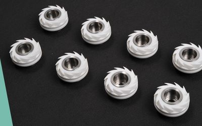
The client, one of the world's leading manufacturer of automation machines, found RPWORLD to provide qualified prototypes and low volume solutions for monthly order of 40 units. They had a new tooling machine under R&D stage, a key component, the impeller assembly failed, which caused delay of the whole product development process.So the client contacted RPWORLD to address the delay problem.
