PCB Via: Essential Guide to Vertical Interconnect Access in Circuit Boards
Printed Circuit Board Vertical Interconnect Access (PCB VIAs) are small plated holes that create electrical connections between different circuit board layers. This article delves into the various types, functions, and best practices of PCB VIAs to help you optimize your PCB design.

Last updated on 28 Aug, 2024. 23 minutes read
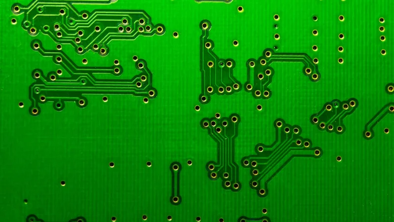
PCB with Via Traces
Introduction
A via, short for Vertical Interconnect Access, is an essential component of a printed circuit board (PCB) that creates electrical connections between different PCB layers. This small copper-plated hole is drilled or laser-cut through the PCB laminates, intersecting two or more adjoining layers. Comprising a barrel, a pad, and an anti-pad, the via facilitates the flow of electrical and thermal currents across the board.
Vias are crucial for multilayered PCB design and production, especially in modern electronics where miniaturization and complex routing are key. They allow signals and power to traverse the board's thickness, enabling the intricate connections required by sophisticated electronic devices. By utilizing the full three-dimensional space of the PCB, vias help designers maximize functionality within compact spaces.
Beyond their role in connecting layers, vias significantly influence signal integrity, power distribution, and overall PCB performance. They are vital for controlling impedance, reducing electromagnetic interference, and ensuring efficient power delivery across the board. In summary, vias are indispensable in the creation of complex multilayer PCBs, playing a central role in the advancement of modern electronics.
Essential Components and Fabrication Process
The process of creating vias begins with the placement of copper pads on each layer of the PCB. A hole is then drilled through these pads, penetrating the board's layers. To prepare the internal layers for electrical conductivity, a chemical solution is used to dissolve the epoxy, exposing the internal copper pads.
The drilled hole is made conductive through electroplating or by inserting copper cylinders into the hole. The inner part of the via typically contains a non-conductive material, often air, while the outer layer is plated with conductive material to establish electrical connections between the layers. By stacking and connecting multiple layers with vias, engineers can create smaller, lighter, and more efficient PCBs, which are essential for modern electronic devices.
Components of a Via
A via consists of three primary components: the barrel, the pad, and the antipad. Each plays a crucial role in ensuring the reliability and functionality of the via.
Barrel: The barrel is a conductive tube that fills the drilled hole, creating an electrical connection between the top, bottom, and, if applicable, the internal layers of the board. The strength of the barrel is often determined by the aspect ratio, which is the ratio of the hole diameter (D) to the barrel length (L).
Pad: The pad, or annular ring, is a circular copper area that connects the barrel to the traces or components on the PCB. It serves as the link between the via and the electrical pathways on the board's surface.
Antipad: The antipad is a void area surrounding the barrel, designed to isolate the via from non-connected layers. It prevents unwanted signal traces from interfering with the electrical connection established by the via.
Recommended reading: What are Vias in Pad? Advantages, Limitations, Applications, and Comparison with Conventional Vias
Demystifying PCB Vias: Types and Functions
Vias differ in size, pad shapes, and hole diameters, each tailored to specific PCB requirements. The main types are through-hole, blind, and buried vias, with others including skip vias, stacked vias, staggered vias, microvias, and vias in pad.
The choice of via depends on the PCB technology, circuitry needs, and budget. For example, while microvias are favored for their smaller size, they are more costly and complex to fabricate than mechanically drilled through-hole vias. However, for high-density interconnect boards, microvias are often the preferred option.
Here's a closer look at the different via types:
Through-Hole Vias: The Backbone of Multilayer Connectivity
Through-hole vias are cylindrical holes that penetrate all layers of a PCB and are plated with conductive material, typically copper. They establish electrical connections between various layers of the board. The process involves drilling holes at specified locations, then applying electroless copper deposition and electrolytic copper plating to ensure consistent conductivity.
Through-hole vias offer several advantages in PCB design:
Robust connections: They provide strong mechanical and electrical connections between layers.
Heat dissipation: Their structure allows for better heat transfer, aiding in thermal management.
Ease of testing: Through-holes are accessible from both sides of the board, facilitating easier testing and rework.
Component mounting: They can be used for mounting through-hole components, which are still preferred in some applications for their reliability.
However, through-hole vias also have limitations:
Space consumption: They occupy space on all layers, reducing the available routing area.
Drill size limitations: Minimum drill sizes are larger compared to other via types, limiting density.
Signal integrity challenges: At high frequencies, they can act as stubs, causing signal reflections.
Typical use cases for through-hole vias include:
Power and ground connections, where their current-carrying capacity is beneficial
Mounting points for through-hole components like connectors or high-power devices
Signal routing in less dense areas of the board
Thermal management, acting as heat conduits between layers
Recommended reading: Through Hole vs Surface Mount: Unveiling the Optimal PCB Assembly Technique
Blind Vias: Connecting Surface to Inner Layers
Blind vias are partial holes that connect an outer layer of a PCB to one or more inner layers, but do not extend through the entire board. Unlike through-hole vias, blind vias are visible only on one side of the PCB. They are typically created using controlled-depth drilling or laser ablation techniques, followed by plating to establish electrical connectivity.
The benefits of using blind vias in high-density designs are significant:
Increased routing density: By not occupying space on all layers, blind vias free up valuable real estate for additional traces and components.
Improved signal integrity: Shorter via lengths reduce parasitic capacitance and inductance, enhancing high-frequency performance.
Enhanced design flexibility: Designers can optimize layer-to-layer connections without impacting the entire stack-up.
Reduced manufacturing costs: For complex boards, blind vias can reduce the overall layer count, potentially lowering production expenses.
Blind vias are particularly useful in several applications:
Mobile devices: Smartphones and tablets benefit from the space-saving properties of blind vias, allowing for more compact designs.
High-speed digital circuits: Data centers and networking equipment use blind vias to maintain signal integrity in dense, high-frequency layouts.
Wearable technology: Fitness trackers and smartwatches leverage blind vias to achieve miniaturization while maintaining functionality.
Aerospace and defense: Blind vias enable the creation of sophisticated, multi-layer boards for radar and communication systems in confined spaces.
Buried Vias: Hidden Connections for Complex Designs
Buried vias are conductive pathways that connect two or more internal layers of a multilayer PCB without extending to either outer surface. These hidden interconnects are completely encapsulated within the board, invisible from the exterior. Buried vias are characterized by their ability to create direct connections between specific internal layers, offering unparalleled design flexibility for complex circuits.
The manufacturing process for buried vias presents several challenges:
Sequential lamination: Each set of buried vias requires a separate drilling and plating process, followed by lamination of additional layers. This multi-step approach increases production time and complexity.
Precise alignment: Ensuring accurate alignment of buried vias across multiple lamination cycles demands advanced registration techniques.
Quality control: Inspection of buried vias is more difficult, often requiring specialized X-ray equipment to verify proper formation and connectivity.
These challenges contribute to higher manufacturing costs compared to through-hole or blind vias. The increased expense is primarily due to longer production times, additional processing steps, and the need for more sophisticated equipment.
Despite the manufacturing complexities, buried vias offer significant advantages:
Enhanced signal integrity: By creating shorter, more direct paths between layers, buried vias minimize signal reflections and reduce crosstalk, crucial for high-speed designs.
Improved EMI performance: The internal nature of buried vias helps contain electromagnetic emissions, enhancing overall EMC compliance.
Optimized board real estate: Buried vias free up valuable surface area and inner layer space, allowing for higher component density and more efficient routing.
Design flexibility: They enable complex interconnection schemes that would be impossible with traditional through-hole vias alone.
Microvia Technology: Pushing the Boundaries of Miniaturization
Microvias, with diameters typically less than 150 micrometers, are essential for high-density interconnect (HDI) designs. They enable complex, multi-layer PCBs with higher connection densities than traditional vias, facilitating intricate routing for advanced electronic devices in smaller form factors.
Manufactured mainly through laser drilling, microvias are created with precision compared to mechanical drilling. The process includes:
Laser Ablation: A focused laser removes material to form the via hole.
Cleaning: Residue is removed with chemical or plasma methods.
Metallization: The via is plated with copper for electrical connectivity.
Filling: Depending on the application, the via may be filled with conductive or non-conductive material.
Laser drilling allows for vias as small as 50 micrometers in diameter and aspect ratios up to 1:1.
Microvias significantly impact miniaturization by enabling:
Higher Component Density: More connections in a smaller area.
Thinner PCBs: Stacked or staggered microvias reduce the number of layers.
Improved Signal Integrity: Shorter connection paths minimize signal degradation.
Enhanced Power Distribution: Increased vias for power and ground improve performance.
Applications of microvias include:
Smartphones: Integrate multiple functions in slim designs.
Wearable Devices: Compact fitness trackers and smartwatches.
Automotive Electronics: Advanced driver assistance systems and infotainment.
5G Infrastructure: High-frequency, high-density designs for base stations.
Medical Implants: Miniaturized devices like pacemakers and cochlear implants.
Recommended reading: Microvias: Pioneering the Future of PCB Design and Electronics Miniaturization
Via in Pads
Vias in Pad are a specific type of via used in PCB design where the via is directly placed within the pad of a surface-mounted component. This approach is often employed in high-density designs to save space and improve electrical performance. By placing the via within the pad, designers can create shorter and more direct connections between layers, which helps minimize signal loss and enhance power distribution. This technique is particularly useful in high-frequency applications where maintaining signal integrity is critical. However, Vias in Pad require careful manufacturing techniques to prevent issues like solder wicking, which can lead to poor connections.
They can either be regular through-hole vias or microvias, but what makes them peculiar is how they are positioned in a surface mount pad. The applications of via-in-pads are mostly with ball grid array (BGA) components.
Designing with Precision: PCB Via Considerations
When designing PCBs, precision in via selection is crucial for optimal performance. Vias connect different layers of a circuit board and impact factors like signal integrity, power distribution, and board density. Considerations include via size, type (through-hole, blind, buried, microvia), and placement to ensure efficient routing and minimize interference. Proper via design enhances overall board functionality and reliability.
Via Size and Aspect Ratio: Balancing Performance and Manufacturability
In PCB design, via size and aspect ratio significantly affect electrical performance, manufacturability, and reliability. Smaller vias enable higher component density and complex routing but may increase resistance and inductance, and are prone to solder wicking. Larger vias enhance current flow and heat dissipation, benefiting high-power applications but reduce available routing space. Balancing via size with performance needs is crucial for optimizing both density and functionality.
Selecting appropriate via sizes based on the board thickness and layer count involves several key guidelines:
Board Thickness:
For thinner boards (up to 1.6 mm), vias can be smaller (e.g., 0.3 mm diameter).
For thicker boards (over 2.0 mm), larger vias (e.g., 0.5 mm or greater) are advisable to ensure adequate current carrying capacity.
Layer Count:
Multi-layer designs (4 layers or more) often benefit from blind or buried vias to reduce signal path lengths, enhancing performance.
For high-density interconnect (HDI) designs, consider a mix of microvias and standard vias to optimize the layout.
Application Requirements:
Power distribution circuits typically require larger vias to handle higher currents, while signal traces can utilize smaller sizes.
Consider environmental factors (e.g., thermal cycling) which might influence via reliability and performance over time.
The following table provides a comparison of recommended via sizes and aspect ratios for different PCB applications:
Via Type | Typical Diameter | Recommended Aspect Ratio | Common Applications |
Through-hole | 0.3 - 6.35 mm | Up to 8:1 | General-purpose PCBs, power distribution |
Blind | 0.1 - 0.3 mm | Up to 1:1 | Mobile devices, high-density boards |
Buried | 0.1 - 0.3 mm | Up to 1:1 | Complex multilayer PCBs, high-speed designs |
Microvia | 0.05 - 0.15 mm | Up to 1:1 | HDI designs, smartphones, wearables |
Via Placement Strategies: Optimizing Signal Integrity and Power Distribution
In high-speed digital designs, proper via placement is crucial for maintaining signal integrity and optimizing power distribution. Best practices include minimizing the number of vias in high-speed signal paths to reduce discontinuities and reflections. When vias are necessary, they should be placed as close as possible to the signal source or load to minimize stub lengths. For differential pairs, symmetrical via placement is essential to maintain pair balance and reduce common-mode noise.
Via fencing is a technique used to control electromagnetic interference (EMI) in PCB designs. It involves placing a series of grounded vias around sensitive signal traces or entire circuit blocks. These vias act as a Faraday cage, containing electromagnetic fields and preventing them from radiating to other parts of the board or external environment. Via fencing is particularly effective in isolating high-frequency circuits, such as clock generators or RF modules, from more sensitive analog components.
For power integrity, strategic via placement in power and ground planes is critical. Techniques include:
Via stitching: Placing multiple vias connecting power and ground planes at regular intervals to reduce plane impedance and improve current flow.
Decoupling via arrays: Clustering vias near decoupling capacitors to minimize the loop inductance between power and ground.
Star-point grounding: Using a central ground via as a reference point for sensitive analog circuits to minimize ground loops.
Examples of via placement patterns for different PCB design scenarios include:
High-speed signal routing: Vias are placed at the ends of traces to minimize stub lengths, with ground vias nearby for return current paths.
BGA fanout: A grid of vias is used to route signals from dense BGA packages to inner layers, often employing micro-vias for HDI designs.
Power distribution: Large vias or via arrays are placed near high-current components, with smaller vias distributed across the board for local power delivery.
EMI sensitive areas: A fence of ground vias surrounds sensitive circuits, with additional vias placed at regular intervals within the enclosed area.
A typical PCB layout example illustrating effective via placement strategies would show:
Signal layer: High-speed traces with minimal vias, and where necessary, vias placed at trace endpoints.
Power plane: Large vias near power-hungry components, with smaller vias distributed across the plane.
Ground plane: Dense via stitching, especially around the board edges and between different ground domains.
Component layer: Decoupling capacitors with nearby via pairs connecting to power and ground planes.
Overall layout: Via fences surrounding sensitive circuit blocks, with clear separation between analog and digital sections.
Thermal Management: Leveraging Vias for Heat Dissipation
Thermal vias are essential for managing heat in PCBs, directing it from high-power components to cooler areas or heat sinks. Filled with thermally conductive material, they are strategically placed beneath components like processors and voltage regulators. By efficiently dissipating heat, thermal vias help maintain optimal temperatures, enhance reliability, and prevent thermal failures.
When designing thermal via arrays, several key considerations must be taken into account:
Via density: Higher density generally improves heat dissipation but may impact manufacturability and cost.
Via size: Larger vias conduct more heat but occupy more board space.
Plating thickness: Thicker copper plating enhances thermal conductivity.
Fill material: Solid copper-filled vias offer the best thermal performance but are more expensive than non-filled or partially filled alternatives.
Thermal plane connection: Ensuring proper connection to thermal planes on multiple layers maximizes heat spreading.
Guidelines for sizing and placing thermal vias for optimal heat dissipation include:
Via diameter: Use the largest practical diameter, typically ranging from 0.3mm to 1.0mm.
Via spacing: Place vias as close together as manufacturing tolerances allow, usually 0.5mm to 1.0mm center-to-center.
Array size: Extend the via array beyond the component's thermal pad by at least 1mm in all directions.
Number of vias: Use as many vias as possible within the available space, considering the trade-off between thermal performance and manufacturing complexity.
Layer connection: Connect thermal vias to copper planes on multiple layers to maximize heat spreading.
A thermal simulation case study highlights the effectiveness of thermal vias in managing heat. A high-power LED module dissipating 5W on a 4-layer PCB showed a junction temperature of 125°C without thermal vias. Adding 25 thermal vias reduced the temperature to 85°C, a 32% decrease. Increasing the vias to 49 further lowered the temperature to 75°C. This study demonstrates how thermal vias can significantly enhance heat dissipation, extending component lifespan and improving system reliability in high-power PCB designs.
Manufacturing Excellence: PCB Via Production Techniques
Drilling and Plating: The Foundation of Via Creation
Creating through-holes in PCBs starts with mechanical drilling using high-speed spindles equipped with tungsten carbide drill bits, rotating at 50,000 to 300,000 RPM. The PCB is securely positioned, and computer-controlled machinery precisely drills each hole, removing material from all layers. Air or lubricant is often used to manage heat and debris.
After drilling, the via walls undergo copper plating. The process begins with electroless copper plating, which deposits a thin, uniform copper layer on the non-conductive surfaces of the hole. This involves cleaning, conditioning, catalyzing with palladium ions, and immersing the board in an electroless copper solution.
Next, electrolytic copper plating builds up the copper thickness. The board is submerged in an electrolyte solution, and an electric current is applied, causing copper to deposit on the via surfaces. This continues until the desired copper thickness, typically 25-35 microns for standard PCBs, is achieved.
Challenges in via drilling and plating include maintaining hole accuracy and consistency across large panels, preventing drill bit breakage and minimizing wear, ensuring uniform plating thickness in high aspect ratio holes, and managing thermal stress during drilling to prevent delamination. To address these issues, quality control measures such as regular inspection and replacement of drill bits, X-ray inspection for hole positioning and quality, cross-sectioning of plated holes to check copper thickness, and electrical testing to ensure proper connectivity are implemented.
Laser Drilling: Precision Technology for Microvia Formation
Laser drilling technology has transformed PCB manufacturing by enabling the precise creation of small vias, with diameters as small as 25 microns. This non-contact method uses focused laser beams, making it ideal for microvias in high-density interconnect (HDI) boards, where traditional drilling falls short.
In PCB manufacturing, two primary types of lasers are commonly used: CO2 lasers and UV lasers. CO2 lasers, operating at a wavelength of 10.6 microns, are particularly effective for drilling through organic materials like epoxy resin. They are widely employed for creating blind vias in multilayer boards. On the other hand, UV lasers, with wavelengths around 355 nm, are capable of drilling through both organic and inorganic materials, including copper. These lasers excel in creating smaller, more precise holes and are often used for drilling through thin copper layers.
Each laser type serves specific applications. CO2 lasers are preferred for drilling larger vias (greater than 75 microns) and are cost-effective for processing organic materials. UV lasers are ideal for ultra-small vias (less than 75 microns), drilling through copper layers, and achieving higher precision in high-density interconnect (HDI) boards.
However, while laser drilling offers significant advantages, there are also limitations and considerations to keep in mind. The heat generated by the laser can affect the surrounding material, potentially causing delamination or degradation, a concern known as the heat-affected zone. Additionally, not all materials are suitable for laser drilling due to their optical or thermal properties. The cost of laser drilling equipment is generally higher than that of mechanical drilling systems, and for larger hole sizes, mechanical drilling may offer faster and more cost-effective throughput.
Comparison of mechanical drilling vs. laser drilling for via formation:
Aspect | Mechanical Drilling | Laser Drilling |
Minimum via size | ~100 microns | ~25 microns |
Precision | Good | Excellent |
Speed for large holes | Fast | Slower |
Speed for small holes | Slow | Fast |
Tool wear | High | None (non-contact) |
Initial equipment cost | Lower | Higher |
Suitable materials | All PCB materials | Limited by material properties |
Heat-affected zone | Minimal | Present, requires management |
Flexibility for different hole sizes | Limited by drill bit sizes | Highly flexible |
Via Filling and Capping: Enhancing Reliability and Performance
Via filling is a process used to enhance the reliability and performance of PCBs by filling the hollow core of vias with specialized materials. Two primary methods are employed:
Conductive Filling: Utilizes materials like conductive epoxy or copper paste to create a solid conductive path through the via. This method is particularly useful for high-frequency applications and thermal management.
Non-Conductive Filling: Employs non-conductive epoxy resins to provide mechanical strength and prevent the ingress of contaminants. This method is often used in multilayer boards to create a planar surface for subsequent layers.
Filled vias in PCB design provide several key benefits, including improved reliability, enhanced signal integrity, increased current capacity, and better thermal management. By reducing susceptibility to thermal cycling stress and offering greater resistance to chemical processes during manufacturing, filled vias contribute to the overall durability of the board. Conductive fillings within the vias help reduce inductance, which is crucial for improving high-frequency performance. Additionally, solid copper fillings boost the current-carrying capacity of vias, making them suitable for high-power applications, while also enhancing heat dissipation.
To ensure a flat, uniform surface over filled vias, various capping techniques are employed. Copper capping involves plating a thin copper layer over the filled via, providing a conductive surface for additional circuitry or component placement. Epoxy capping, on the other hand, uses a non-conductive epoxy to create a smooth, insulated surface. Solder mask capping involves covering the filled via with the solder mask layer, protecting the filling material, and ensuring a flat surface. These capping techniques are crucial for maintaining consistency in areas with high via density and safeguarding the via filling during further manufacturing processes.
Pushing Boundaries: Advanced PCB Via Applications
High-Frequency Design: Vias in RF and Microwave Circuits
In high-frequency PCB designs, vias pose challenges due to their parasitic effects. As frequencies rise, vias can cause signal reflections, increased insertion loss, and reduced signal integrity by acting as discontinuities in transmission lines. The main issues are managing via inductance, capacitance, and resonance, which become more problematic at higher frequencies.
To minimize via inductance and capacitance in RF circuits, several techniques are employed:
Via size optimization: Smaller diameter vias generally have lower inductance and capacitance.
Via stub removal: Backdrilling or buried vias eliminate unused portions of the via barrel, reducing parasitic effects.
Ground via fencing: Surrounding signal vias with ground vias helps control impedance and reduce crosstalk.
Impedance matching: Careful design of the via and its surrounding structures to match the characteristic impedance of the transmission line.
Examples of via structures optimized for high-frequency performance include:
Tapered vias: Gradually changing the via diameter to match impedance and reduce reflections.
Compensated via pads: Adjusting the size and shape of via pads to counteract parasitic capacitance.
Blind and buried vias: Minimizing via length to reduce inductance and improve signal integrity.
Air-core vias: Removing dielectric material around the via to reduce capacitance in critical areas.
Embedded Components: Integrating Passives with Via Technology
Embedded passive components represent an innovative approach to PCB design, utilizing via structures to create resistors, capacitors, and inductors directly within the board layers. This technology leverages the conductive and dielectric properties of PCB materials to form functional passive elements, reducing the need for surface-mounted components.
Resistors, capacitors, and inductors can be created using specialized via designs:
Resistors: Formed by creating a via with a specific length and diameter, filled with a resistive material. The resistance value is determined by the via's dimensions and the material's resistivity.
Capacitors: Constructed using two conductive plates (typically copper layers) separated by a dielectric material. The capacitance is controlled by the plate area and the dielectric thickness.
Inductors: Created by forming spiral patterns on adjacent layers, connected by vias. The inductance value depends on the number of turns, spiral diameter, and layer spacing.
Advantages of using embedded components in PCBs include:
Reduced board size and weight
Improved signal integrity due to shorter connection paths
Enhanced reliability by eliminating solder joints
Increased design flexibility and component density
Better performance at high frequencies
Challenges associated with embedded components:
Limited range of achievable values compared to discrete components
Increased complexity in PCB design and manufacturing
Potential for higher initial production costs
Difficulty in testing and replacing faulty embedded components
Examples of embedded component designs:
Embedded decoupling capacitors: Placed directly under BGA packages to minimize power supply noise.
Resistor networks: Arrays of embedded resistors for termination in high-speed digital circuits.
Spiral inductors: Used in RF circuits for impedance matching and filtering.
Performance characteristics of these designs often include improved high-frequency response, reduced parasitic effects, and better thermal management compared to surface-mount equivalents.
Comparison table of traditional surface-mount components vs. embedded via-based components:
Aspect | Surface-Mount Components | Embedded Via-Based Components |
Size | Larger footprint | Minimal surface footprint |
Value Range | Wide range available | Limited range, less precise |
Cost | Lower for small quantities | Lower for high-volume production |
Design Flexibility | Easy to modify or replace | Fixed after manufacturing |
High-Frequency Performance | Good | Excellent (shorter connections) |
Reliability | Subject to solder joint failures | Higher (no solder joints) |
Thermal Management | Can create hot spots | Better heat distribution |
Testing and Rework | Straightforward | Challenging |
Manufacturing Complexity | Standard PCB processes | Requires specialized processes |
3D Printed Electronics: Redefining Via Creation
3D printed electronics represent a paradigm shift in PCB manufacturing, offering unprecedented freedom in via design and creation. This additive manufacturing approach allows for the layer-by-layer deposition of conductive and dielectric materials, enabling the formation of complex, three-dimensional structures that were previously impossible with traditional PCB fabrication methods.
Additive manufacturing techniques create unique via structures by:
Direct printing of conductive paths: Vias can be formed as continuous structures during the printing process, eliminating the need for drilling and plating.
Embedded via creation: Vias can be integrated into the PCB structure as it's being built, allowing for complex internal routing.
Material gradient printing: The conductivity and dielectric properties of vias can be varied along their length, enabling new functional possibilities.
Non-linear via paths: Vias are no longer limited to straight vertical paths, allowing for curved or angled interconnects.
The potential advantages of 3D printed vias include:
Enhanced design flexibility: Vias can be placed and shaped with fewer constraints.
Improved signal integrity: Custom-shaped vias can be optimized for specific electrical characteristics.
Reduced manufacturing steps: Elimination of drilling and plating processes for via formation.
Increased component density: Complex 3D routing allows for more efficient use of board space.
Customization at scale: Each via can be uniquely designed without increasing production complexity.
Examples of innovative via designs enabled by 3D printing technology:
Helical vias: Spiral-shaped vias that can function as both interconnects and inductors.
Tapered vias: Vias with gradually changing diameters to optimize impedance matching.
Branching vias: Single vias that split into multiple paths, reducing the need for separate connections.
Embedded sensor vias: Vias integrated with sensing elements for structural health monitoring.
Troubleshooting and Quality Assurance: Ensuring Via Reliability
Common Via Defects: Identification and Prevention
Common via defects in PCB manufacturing include:
Voids: Air pockets or gaps within the via plating or filling material. Causes: Insufficient plating solution penetration, gas entrapment during plating. Impact: Reduced current-carrying capacity, potential open circuits. Prevention: Optimize plating parameters, use vacuum plating techniques.
Cracks: Fractures in the via barrel or at the via-to-pad interface. Causes: Thermal stress, mechanical stress during drilling or assembly. Impact: Intermittent connections, complete failure under thermal cycling. Prevention: Use appropriate via aspect ratios, implement stress-relief designs.
Misalignment: Vias not properly centered on pads or between layers. Causes: Registration errors during drilling or layer lamination. Impact: Reduced connection reliability, potential short circuits. Prevention: Improve drilling accuracy, use fiducial markers for alignment.
Copper Wicking: Excess copper plating extending beyond the via barrel. Causes: Overplating, insufficient etch-back process. Impact: Potential short circuits between layers. Prevention: Optimize plating time, implement proper etch-back procedures.
Resin Smear: Dielectric material smeared over the inner layer connections. Causes: Heat generated during drilling, inadequate desmear process. Impact: Poor electrical connection between via and internal layers. Prevention: Optimize drilling parameters, enhance desmear process.
Barrel Fatigue: Separation of the plated barrel from the via wall. Causes: Repeated thermal cycling, CTE mismatch between materials. Impact: Intermittent or open connections, especially in high-reliability applications. Prevention: Use via-in-pad designs, implement proper thermal management.
Strategies for preventing via defects during design and manufacturing:
Design for Manufacturability (DFM):
Adhere to recommended aspect ratios for vias
Implement thermal relief patterns for large copper areas
Use stacked or staggered vias for high-current applications
Process Control:
Maintain strict control over drilling parameters (speed, feed rate)
Optimize plating bath chemistry and process parameters
Implement robust cleaning and desmear processes
Material Selection:
Choose PCB materials with appropriate CTE characteristics
Use high-Tg materials for applications with wide temperature ranges
Quality Control:
Implement statistical process control (SPC) for critical parameters
Perform regular maintenance and calibration of manufacturing equipment
Microscope images or X-ray scans of via defects would typically show:
Voids: Dark spots or bubbles within the via barrel in X-ray images.
Cracks: Fine lines or fractures visible in cross-sectional microscope images.
Misalignment: Offset between via barrel and pads visible in top-down microscope views.
Copper Wicking: Irregular copper growth extending from via barrels in cross-sections.
Resin Smear: Thin layer obscuring copper layers in via cross-sectional images.
Barrel Fatigue: Separation between plating and via wall visible in cross-sectional views.
Via Testing and Inspection: Verifying Interconnect Integrity
Via integrity testing is crucial for ensuring reliable PCB interconnections. Common methods include:
Continuity Testing: Measures electrical continuity between via endpoints using a multimeter or specialized test equipment. This basic test detects open circuits but may miss partial defects.
Time-Domain Reflectometry (TDR): Sends high-frequency pulses through vias and analyzes reflected signals. TDR can detect impedance discontinuities, helping identify defects like voids or cracks.
Four-Wire Kelvin Testing: Provides accurate resistance measurements of vias, useful for detecting subtle defects that affect conductivity.
High-Potential (HiPot) Testing: Applies high voltage between layers to detect insulation breakdowns or near-shorts in via structures.
Non-destructive inspection techniques offer detailed insights without damaging the PCB:
X-ray Inspection: Provides internal views of via structures, revealing voids, misalignments, and plating inconsistencies. Advanced 3D X-ray systems offer detailed volumetric analysis of via defects.
Cross-sectioning: While destructive to the specific area examined, it provides high-resolution images of via structures when performed on test coupons or sacrificial boards from the same production batch.
Ultrasonic Imaging: Uses sound waves to detect delaminations or voids within via structures, particularly effective for thick PCBs.
Automated Optical Inspection (AOI) plays a critical role in via quality control:
High-resolution cameras capture detailed images of via surfaces and surrounding areas.
Advanced pattern recognition algorithms detect defects such as misalignments, copper splashes, or incomplete filling.
AOI systems can inspect large quantities of vias rapidly, making 100% inspection feasible in production environments.
Integration with statistical process control (SPC) systems allows for real-time monitoring of via quality trends.
Guidelines for interpreting via test results and acceptance criteria:
Continuity Testing: Resistance values should fall within specified ranges, typically less than 1 ohm for standard vias.
TDR Results: Reflection coefficients exceeding ±10% may indicate significant defects requiring further investigation.
X-ray Inspection: Void content should typically not exceed 25% of the via barrel volume, with no single void larger than 10%.
AOI Criteria: Set threshold values for via diameter, annular ring width, and registration accuracy based on IPC standards or specific design requirements.
Sample test report for via quality assessment:
Test Type: X-ray Inspection Board ID: PCB-2024-001 Via Type: Through-hole Sample Size: 1000 vias
Results:
98.5% of vias pass all criteria
1.2% show minor voids (<10% of barrel volume)
0.3% exhibit misalignment (within acceptable limits)
No critical defects detected
Conclusion: Batch meets quality standards; proceed with production.
Conclusion
PCB vias play a crucial role in modern electronics, enabling the creation of complex multilayer designs that power our increasingly sophisticated devices. From traditional through-hole vias to advanced microvia technologies, these interconnects are fundamental to achieving high-density, high-performance circuit boards. The ongoing developments in via technology, such as 3D printed vias and embedded passive components, are pushing the boundaries of what's possible in PCB design. As electronics continue to evolve, with demands for higher speeds, smaller form factors, and improved reliability, the importance of optimized via design cannot be overstated. Engineers and designers must consider via selection and placement as critical aspects of their PCB projects, as these decisions significantly impact signal integrity, power distribution, and overall board performance.
Frequently Asked Questions
Q: What is the difference between a through-hole via and a blind via? A: A through-hole via extends through all layers of the PCB, while a blind via connects an outer layer to one or more inner layers but does not go through the entire board.
Q: How do I choose the right via size for my PCB design? A: Via size selection depends on factors such as board thickness, current requirements, and manufacturing capabilities. Generally, aim for the smallest via size that meets your electrical and thermal requirements while considering manufacturability.
Q: Can vias affect signal integrity in high-speed designs? A: Yes, vias can introduce discontinuities in transmission lines, causing signal reflections and degradation. Proper via design, including size optimization and stub removal, is crucial for maintaining signal integrity in high-speed circuits.
Q: What are microvias, and when should I use them? A: Microvias are very small vias, typically less than 150 micrometers in diameter. They are used in high-density interconnect (HDI) designs where space is at a premium, such as in smartphones or wearable devices.
Q: How can I prevent via failures in my PCB design? A: To prevent via failures, consider factors such as proper aspect ratio, thermal management, use of teardrops for improved connection strength, and adherence to manufacturing guidelines. Regular inspection and testing during production are also crucial.
Q: What is via tenting, and when is it used? A: Via tenting involves covering vias with solder mask to protect them from environmental factors or to prevent solder wicking during assembly. It's commonly used for vias that don't require electrical connection on the outer layers.
Q: How do buried vias differ from blind vias, and what are their advantages? A: Buried vias connect internal layers without reaching the board's surface, while blind vias connect an outer layer to internal layers. Buried vias offer better signal integrity and allow for higher routing density, but they can be more complex and expensive to manufacture.
Reference
1. Proto Electronics. How and Where to Use Vias in PCB Design. 2021. Available from: https://www.google.com/amp/s/www.proto-electronics.com/blog/how-and-where-use-vias-in-pcb-design%3fhs_amp=true
2. Our PCB. PCB Via: What is it, and Which Type Should You Choose? 2022. Available from: https://www.ourpcb.com/pcb-via.html
3. PCB GOGO. PCB Vias: Types, Design, Covering. 2022. Available from: https://www.pcbgogo.com/Article/PCB_Vias__Types__Design__Covering.html
4. OUR PCB. Blind Via PCB - What Should You Know. 2022. Available from: https://www.ourpcb.com/blind-via-pcb.html
5. Circuit Digest. Understanding Blind, Buried and Through-hole Vias in PCB. 2021. Available from: https://circuitdigest.com/article/understanding-blind-buried-and-through-hole-vias-in-pcb
6. PCB Directory. What are Stacked Microvias? 2022. Available from: https://www.pcbdirectory.com/community/what-are-stacked-microvias
7. PCB HERO. Staggered Microvias and Stacked Microvias PCB. 2022. Available from: https://www.pcb-hero.com/blogs/lilycolumn/staggered-microvias-and-stacked-microvias-pcb
8. PCB Online. 8 Types of PCB Vias - A Complete Guide of PCB Vias in 2022. 2022. Available from: https://www.pcbonline.com/blog/pcb-vias-and-their-types.html
9. Cadence. Microvias in Printed Circuit Design Are an HDI Necessity. 2022. Available from: https://resources.pcb.cadence.com/blog/2022-microvias-in-printed-circuit-design-are-an-hdi-necessity
10. MacroFab. Via in Pad PCB Design. 2022. Available from: https://macrofab.com/blog/via-in-pad-pcb-design/#:~:text=Via%20in%20pad%20is%20the,reduce%20the%20PCBs%20overall%20size
11. RayMing. What is the Role of Via in PCB - Printed Circuit Board Manufacturing and PCB Assembly? 2021. Available from: https://www.raypcb.com/via-in-pcb/
in this article
1. Introduction 2. Essential Components and Fabrication Process3. Demystifying PCB Vias: Types and Functions4. 5. Designing with Precision: PCB Via Considerations6. Manufacturing Excellence: PCB Via Production Techniques7. Pushing Boundaries: Advanced PCB Via Applications8. Troubleshooting and Quality Assurance: Ensuring Via Reliability9. Conclusion10. Frequently Asked Questions11. Reference