PCB Solder Mask: Everything You Need to Know
The purpose of this article is to provide a comprehensive, in-depth guide to PCB soldermask, exploring the key concepts, principles, and practical applications that will help you excel in PCB design and manufacturing.

Last updated on 28 Aug, 2024. 22 minutes read
Introduction
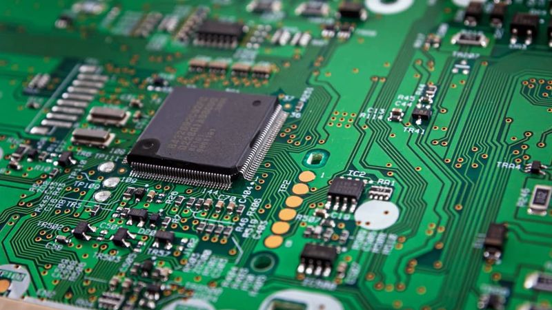
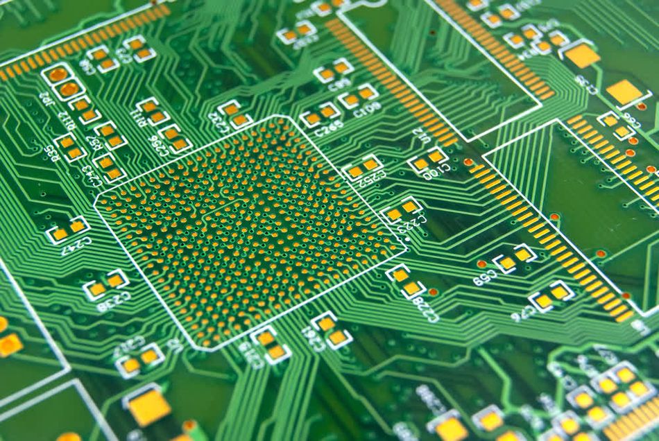
Solder mask, the thin polymer layer applied to printed circuit boards (PCBs), plays a crucial role in modern electronics manufacturing. This protective coating shields copper traces from oxidation, prevents solder bridges during assembly and enhances the overall durability of electronic devices. As PCB designs become increasingly complex and miniaturized, the importance of solder masks in ensuring reliable performance cannot be overstated.
This article delves into the advanced techniques and recent innovations in solder mask technology, catering to engineering professionals in the electronics manufacturing industry. From cutting-edge materials to precision application methods, we explore how solder mask continues to evolve, addressing the challenges of high-density interconnects and demanding operating environments.
The Fundamentals of Solder Mask Technology
Composition and Properties of Modern Solder Masks
Solder masks are typically composed of thermosetting polymers, which provide excellent resistance to heat and chemicals. Like other layers such as copper and silkscreen, the solder mask too, is a distinct PCB layer. The most common types include:
Epoxy-based Solder Masks
Epoxy liquid solder mask consists of a two-component system, typically comprising an epoxy resin and a hardener. When mixed, they create a liquid that can be applied to the surface of the PCB. The primary benefits of epoxy liquid solder mask are its excellent adhesion, good chemical resistance, and cost-effectiveness.
Acrylic-based Solder Masks
Acrylic-based solder masks offer superior flexibility and are often preferred for flex and rigid-flex PCBs. They are composed of acrylic monomers, photoinitiators, and other functional additives.
Urethane-based Solder Masks
Urethane-based solder masks balance epoxy and acrylic properties, offering good flexibility and chemical resistance.
Regardless of the type of solder mask, these materials ensure reliable insulation and protection of solder joints and pads having different types of solder.
Suggested Reading: Types of Solder: A Comprehensive Guide for Engineering Professionals
Essential Properties of Solder Masks
Key properties of solder masks include:
Adhesion: The ability to bond strongly to the PCB substrate and resist peeling or flaking during thermal cycling and mechanical stress.
Thermal Resistance: The capacity to withstand high temperatures during soldering processes and normal operation without degradation.
Dielectric Strength: The maximum electric field the material can withstand without breaking down, crucial for preventing short circuits.
Chemical Resistance: The ability to resist degradation from exposure to various chemicals used in PCB manufacturing and cleaning processes.
Flexibility: Important for flex and rigid-flex PCBs, allowing the solder mask to bend without cracking or delaminating.
Here's a comparison of properties for different solder mask types:
Property | Epoxy-based | Acrylic-based | Urethane-based |
Adhesion | Excellent | Good | Very Good |
Thermal Resistance | High | Moderate | High |
Dielectric Strength | High | Moderate | High |
Chemical Resistance | Excellent | Good | Very Good |
Flexibility | Low | Excellent | Good |
Purpose and Functions in PCB Manufacturing
Solder masks are critical for the performance of printed circuit boards (PCBs). This thin layer of polymer coating serves multiple essential functions that contribute to the overall quality, reliability, and longevity of electronic devices.
Protection
One of the primary purposes of a solder mask is to protect the copper traces on the PCB from oxidation and corrosion. By creating a barrier between the copper and the environment, the solder mask helps maintain the conductivity and integrity of the circuit over time. This protection is particularly important in harsh environments where moisture, chemicals, or other contaminants could potentially degrade the PCB.
Insulation
Solder mask provides electrical isolation between adjacent copper traces, reducing the risk of short circuits and improving the overall reliability of the PCB. This property becomes increasingly important as PCB designs become more compact and complex, with tighter spacing between components and traces.
Solder Flow Control
Solder masks are crucial during PCB assembly as it helps control the flow of solder by preventing it from adhering to areas where it's not needed. This function is crucial in preventing solder bridges, which occur when excess solder creates unwanted connections between adjacent pads or leads.
Enhanced Durability
The presence of a solder mask significantly enhances PCB reliability and longevity. By protecting against environmental factors, reducing the risk of short circuits, and improving solder joint quality, solder mask helps to extend the operational life of electronic devices. It also contributes to the overall durability of the PCB, making it more resistant to mechanical stress and thermal cycling.
Key functions of solder mask in PCB manufacturing include:
Protection of copper traces from oxidation and corrosion
Electrical insulation between adjacent traces and components
Prevention of solder bridges during the assembly process
Definition of precise areas for solder application
Enhancement of PCB visual appearance and component identification
Improvement of PCB resistance to environmental factors
Reduction of electromagnetic interference (EMI) in some applications
Facilitation of automated optical inspection (AOI) processes
Protection against handling damage during assembly and testing
Contribution to overall PCB miniaturization by allowing tighter component spacing
Advanced Solder Mask Application Techniques
Liquid Photoimageable Solder Mask (LPSM) Process
Liquid Photoimageable Solder Mask (LPSM) is a widely adopted advanced technique. It offers high precision and flexibility, making it suitable for complex PCB designs with fine-pitch components and intricate patterns.
The LPSM process involves applying a liquid photosensitive polymer to the PCB surface, which is then selectively cured using ultraviolet (UV) light.
Advantages of LPSM include:
High-resolution and fine-line definition
Excellent adhesion to various substrate materials
Ability to create complex patterns and openings
Compatibility with automated manufacturing processes
Reduced waste compared to traditional screening methods
Recent improvements in LPSM technology include:
Development of low-temperature curing formulations, reducing thermal stress on PCB components.
Introduction of LED-curable solder masks, offering faster processing times and reduced energy consumption.
Advancements in nano-filled solder mask materials, improving thermal management and electrical performance.
Implementation of direct imaging systems, eliminating the need for physical photomasks and enhancing flexibility in design changes.
Integration of additive manufacturing techniques, allowing for 3D-printed solder mask structures on complex PCB topographies.
Dry Film Solder Mask Technology
Dry Film Solder Mask (DFSM) technology offers an alternative approach to applying solder masks on printed circuit boards (PCBs). This method involves using a pre-formed photosensitive film that is laminated onto the PCB surface, as opposed to liquid application methods.
A dry film solder mask is often preferred in the following scenarios:
High-volume production: The faster processing speed and lower material waste make it cost-effective for large-scale manufacturing.
Thick solder mask requirements: DFSM can achieve greater thicknesses in a single application compared to liquid methods.
Boards with large flat areas: The uniform thickness of dry film is particularly advantageous on PCBs with extensive planar surfaces.
Applications requiring precise thickness control: The pre-formed nature of the film ensures consistent thickness across the board.
The dry film process allows for multi-layer application, enabling the creation of very thick solder mask layers when required. This can be achieved by laminating multiple layers of film before exposure and development, resulting in precisely controlled thick solder mask areas for specific design requirements.
Excellent thickness control and uniformity of DFSM contribute to improved yields in PCB manufacturing, particularly for boards with tight tolerances or specific electrical performance requirements.
The following table summarizes the differences between Liquid and Dry film solder mask techniques:
Comparison between dry film and liquid solder mask:
Characteristic | Dry Film Solder Mask | Liquid Solder Mask |
Thickness control | Excellent | Good |
Uniformity | Very high | Moderate to high |
Fine line resolution | Good | Excellent |
Processing speed | Fast | Moderate |
Material waste | Low | Moderate to high |
Initial equipment cost | Moderate | High |
Flexibility in design changes | Limited | High |
Suitability for high-volume production | Excellent | Good |
Emerging Application Methods
These emerging solder mask application methods aim to address the challenges posed by increasingly complex PCB designs and demanding manufacturing requirements.
Inkjet Printing Technology
Inkjet printing represents a promising approach to solder mask application, offering high precision and flexibility.
Key features of inkjet printing technology include:
Non-contact deposition method
Digital control for precise patterning
Potential for multi-material printing
Reduced material waste compared to traditional methods
Recent research at the University of Manchester has demonstrated the feasibility of inkjet-printed solder masks for fine-pitch applications. The study showed that this method could achieve line widths as small as 50 μm, with excellent edge definition and thickness control.
Laser Direct Imaging (LDI) with Photosensitive Solder Mask
LDI technology, combined with advanced photosensitive solder mask materials, offers a maskless approach to solder mask patterning.
Key features of LDI Photosensitive solder mask include:
Eliminates the need for photomasks
High-resolution patterning capabilities
Improved flexibility for design changes
Potential for reduced processing steps
Industry trials by major PCB manufacturers have shown that LDI can achieve line resolutions below 30 μm, surpassing traditional photolithography methods. This technique is particularly promising for high-density interconnect (HDI) boards and advanced packaging applications.
The main challenges include the high initial equipment cost and the need for specialized photosensitive solder mask materials optimized for laser exposure.
3D Printed Solder Mask
Additive manufacturing techniques are being explored for solder mask application, particularly for non-planar PCB surfaces and unique geometries.
Key features:
Ability to create three-dimensional solder mask structures
Customizable thickness and topography
Potential for integrating additional functionalities (e.g., thermal management)
Reduced material waste
Research at the Moscow Aviation Institute has demonstrated the feasibility of 3D-printed solder masks. The method shows the feasibility of 3D solder masks on the inner layers of multilayer PCBs.
Challenges include developing 3D printable materials that meet the stringent requirements for solder mask performance and ensuring consistent quality across large PCB areas.
Design Considerations for Optimal Solder Mask Performance
Solder Mask Clearance and Registration
Solder mask clearance refers to the distance between the edge of a copper pad or trace and the surrounding solder mask. This clearance plays a vital role in preventing solder bridges, ensuring proper component placement, and maintaining the overall integrity of the PCB.
Insufficient clearance can lead to several issues:
Solder bridging: When clearance is too small, solder can spread beyond the intended pad, potentially causing short circuits.
Component placement difficulties: Inadequate clearance can interfere with the proper seating of components on the board.
Reduced electrical isolation: Insufficient clearance may compromise the insulation between adjacent pads or traces.
Increased risk of contamination: Smaller clearances can trap contaminants, leading to potential reliability issues.
Guidelines for solder mask clearance vary depending on the PCB design and component types. Generally, the following principles apply:
For standard through-hole components, a clearance of 50-100 μm (2-4 mils) is typically recommended.
Surface mount technology (SMT) components often require tighter clearances, ranging from 25-75 μm (1-3 mils).
High-density interconnect (HDI) boards may require even tighter clearances, sometimes as low as 15-25 μm (0.6-1 mil).
For high-voltage applications, larger clearances are necessary to maintain proper isolation.
Misregistration, which occurs when the solder mask is not perfectly aligned with the copper pattern, can have significant impacts on PCB functionality:
Exposed copper: Misregistration can leave portions of copper traces or pads exposed, increasing the risk of short circuits or oxidation.
Covered pads: If the solder mask overlaps onto pads, it can interfere with soldering and component placement.
Reduced electrical performance: Misalignment can affect the carefully designed impedance of high-frequency traces.
Aesthetic issues: While not directly impacting functionality, misregistration can lead to a visually unappealing board, which may be a concern for some applications.
To mitigate these issues, PCB designers and manufacturers must adhere to strict tolerances and employ advanced registration techniques. Modern manufacturing processes typically aim for registration accuracies of ±50 μm or better.
The following table provides recommended solder mask clearances for different component types:
Component Type | Minimum Clearance | Optimal Clearance | Maximum Clearance |
Through-hole | 50 μm (2 mils) | 75 μm (3 mils) | 100 μm (4 mils) |
SMT (>0.5 mm pitch) | 25 μm (1 mil) | 50 μm (2 mils) | 75 μm (3 mils) |
SMT (≤0.5 mm pitch) | 15 μm (0.6 mil) | 25 μm (1 mil) | 50 μm (2 mils) |
BGA | 25 μm (1 mil) | 50 μm (2 mils) | 75 μm (3 mils) |
High-voltage (>100V) | 250 μm (10 mils) | 500 μm (20 mils) | 1000 μm (40 mils) |
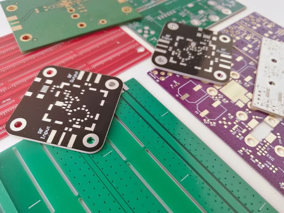
Color Selection and Its Impact
The choice of solder mask color in printed circuit board (PCB) manufacturing is more than just an aesthetic decision. It plays a significant role in both the functional and visual aspects of the final product. While green has long been the standard color for solder masks, the industry has expanded to include a variety of colors, each with its own set of advantages and applications.
The significance of solder mask color choice extends to several areas:
Visual inspection: Different colors can enhance or hinder the visibility of copper traces, solder joints, and other board features during inspection processes.
Thermal properties: Colors can affect the board's heat absorption and reflection characteristics, potentially impacting the thermal management of the PCB.
Light sensitivity: Some colors may be more suitable for applications where the PCB is exposed to light, such as in LED products or outdoor electronics.
Brand identity: Custom colors can be used to reinforce brand identity or meet specific aesthetic requirements for consumer products.
Functional requirements: Certain colors may be preferred or required for specific industries or applications, such as military or aerospace.
The impact of color on heat absorption and reflection is an important consideration in solder mask selection. While there is limited scientific data specifically on solder mask colors, general principles of color physics apply:
Darker colors (e.g., black, dark blue) tend to absorb more heat, which could potentially lead to higher operating temperatures in some applications.
Lighter colors (e.g., white, yellow) generally reflect more heat, potentially aiding in thermal management.
Green, the most common solder mask color, offers a balance between heat absorption and reflection.
It's important to note that the thermal impact of solder mask color is typically minor compared to other factors such as board layout, component selection, and overall thermal management strategies.
While there are no strict industry standards mandating specific colors for solder masks, certain preferences and conventions have emerged.
The following table shows common solder mask colors and their typical applications:
Color | Typical Applications |
Green | The standard for many PCBs, good visibility |
Black | Used for military and high-end boards |
Red | Common in LED circuits |
Blue | Preferred for custom and visible designs |
White | Used for special appearances or designs |
Yellow | Used in decorative or specific application designs |
When selecting a solder mask color, engineers and PCB designers should consider factors such as the intended application, inspection requirements, thermal considerations, and any industry-specific preferences or regulations.
Thickness Control and Its Effects
Solder mask thickness is a critical parameter in printed circuit board (PCB) manufacturing that significantly impacts both the performance and reliability of the final product. Precise control of solder mask thickness is essential for ensuring optimal protection of the PCB while maintaining the necessary electrical and mechanical properties.
The importance of solder mask thickness in PCB manufacturing stems from its multiple functions:
Electrical insulation: The solder mask acts as a dielectric layer, preventing short circuits between adjacent traces and components.
Environmental protection: It shields the copper traces and pads from oxidation and other environmental factors.
Solder control: The thickness of the solder mask influences the amount of solder that can be applied during the assembly process.
Component placement: Proper thickness ensures accurate component seating and alignment.
Suggested Reading: Understanding PCB Thickness: A Comprehensive Guide
Solder mask thickness affects PCB performance and manufacturing processes in several ways:
Impedance control: In high-frequency applications, solder mask thickness can impact the impedance of transmission lines.
Thermal management: The thickness of the solder mask layer affects heat dissipation from components and traces.
Flexibility: For flex and rigid-flex PCBs, the solder mask thickness contributes to the overall flexibility of the board.
Manufacturing yield: Inconsistent or improper thickness can lead to defects such as solder bridging or insufficient coverage.
Recommended thickness ranges for different applications vary, but generally fall within the following guidelines:
Standard PCBs: 20-30 μm (0.8-1.2 mils)
High-density interconnect (HDI) boards: 15-25 μm (0.6-1.0 mils)
Flex and rigid-flex PCBs: 10-20 μm (0.4-0.8 mils)
High-frequency applications: 15-25 μm (0.6-1.0 mils), with tighter tolerances
Power electronics: 30-50 μm (1.2-2.0 mils) for improved thermal management
Quality Control and Testing of Solder Mask
Adhesion and Coverage Testing
Ensuring proper adhesion and complete coverage of solder mask is crucial for the reliability and performance of printed circuit boards (PCBs). Adhesion testing verifies that the solder mask remains firmly attached to the PCB substrate under various conditions, while coverage testing ensures that the solder mask provides adequate protection to all required areas of the board.
Methods for testing solder mask adhesion to the PCB include:
Cross-hatch test: This method involves creating a grid of cuts through the solder mask and applying adhesive tape to test the mask's resistance to peeling.
Tape peel test: A standardized adhesive tape is applied to the solder mask surface and then rapidly removed to assess adhesion strength.
Thermal shock testing: The PCB is subjected to rapid temperature changes to evaluate the solder mask's ability to maintain adhesion under thermal stress.
Chemical resistance test: The board is exposed to various chemicals to ensure the solder mask remains adhered and does not degrade.
Techniques for ensuring complete and uniform coverage include:
Automated optical inspection (AOI): High-resolution cameras and image processing software are used to detect areas of incomplete coverage or defects in the solder mask.
Suggested Reading: What is AOI (Automated Optical Inspection): A Comprehensive Guide
Fluorescence inspection: Some solder mask materials contain fluorescent additives that allow for easy visual inspection under UV light.
Thickness measurement: Optical or mechanical methods are used to verify consistent solder mask thickness across the board.
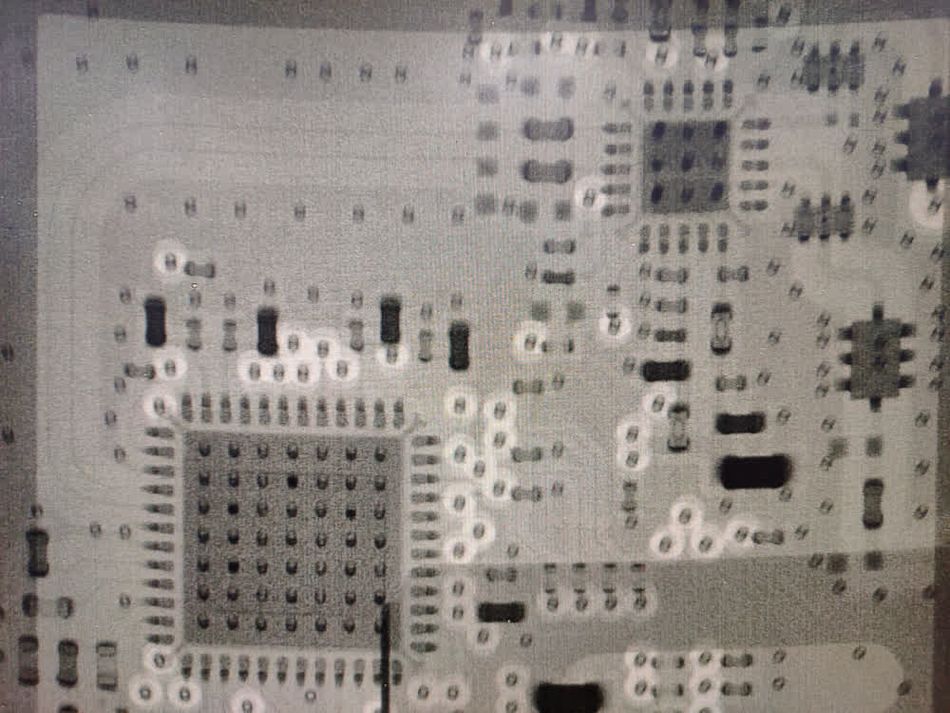
X-ray inspection: For complex multilayer boards, X-ray imaging can reveal any internal coverage issues or voids in the solder mask.
Industry standards for adhesion testing are primarily set by the IPC (Association Connecting Electronics Industries). Key standards include:
IPC-SM-840: Qualification and Performance Specification of Permanent Solder Mask and Flexible Cover Materials
IPC-TM-650: Test Methods Manual, which includes specific procedures for solder mask testing
Electrical and Environmental Testing
Electrical and environmental testing of solder mask is crucial for ensuring the long-term reliability and performance of printed circuit boards (PCBs). These tests simulate various conditions that a PCB might encounter during its operational lifetime and verify that the solder mask maintains its protective and insulating properties.
Electrical tests performed on solder masks primarily focus on their insulation properties. The most common electrical test is the insulation resistance test, which is typically performed by applying a high voltage between closely spaced conductors and measuring the resulting current flow. A high insulation resistance indicates good electrical isolation provided by the solder mask.
Suggested Reading: What Is In-Circuit Testing? An Essential Guide for Engineers
Environmental tests subject the solder mask to various stress conditions to evaluate its durability and performance. Key environmental tests include:
Thermal shock testing: This test involves rapidly cycling the PCB between extreme hot and cold temperatures. It assesses the solder mask's ability to withstand thermal stress without cracking, peeling, or losing adhesion to the substrate.
Humidity resistance testing: The PCB is exposed to high humidity conditions for an extended period. This test evaluates the solder mask's ability to prevent moisture ingress and maintain its protective properties in damp environments.
Salt spray testing: This test simulates exposure to corrosive environments by subjecting the PCB to a salt spray mist. It assesses the solder mask's ability to protect the underlying copper from corrosion.
UV exposure testing: For PCBs that may be exposed to sunlight, this test evaluates the solder mask's resistance to degradation from ultraviolet radiation.
The following table summarizes different tests and their purposes:
Test Type | Purpose |
Insulation Resistance | Verify electrical isolation between conductors |
Thermal Shock | Assess resistance to temperature-induced stress |
Humidity Resistance | Evaluate protection against moisture ingress |
Salt Spray | Test corrosion resistance in harsh environments |
UV Exposure | Determine resistance to UV-induced degradation |
Dielectric Withstanding Voltage | Verify insulation integrity under high-voltage |
Thermal Cycling | Assess long-term reliability under temperature fluctuations |
Chemical Resistance | Evaluate protection against various chemicals and solvents |
By subjecting PCBs to these rigorous electrical and environmental tests, manufacturers can ensure that the solder mask will perform its critical functions throughout the expected lifetime of the product.
Innovations in Solder Mask Technology
High-Temperature Solder Masks
High-temperature solder masks are designed to withstand extreme temperatures, making them suitable for applications in automotive, aerospace, and industrial sectors where standard solder masks would fail.
They are typically formulated with advanced polymer systems that maintain their structural integrity and protective properties at elevated temperatures. The development process involves extensive research into heat-resistant materials, often incorporating ceramic or silicone-based compounds to enhance thermal stability.
Benefits of high-temperature solder masks include:
Increased reliability in extreme environments
Extended PCB lifespan under high-temperature conditions
Improved thermal management capabilities
Enhanced resistance to thermal cycling and shock
Compatibility with lead-free soldering processes that require higher temperatures
While specific technical specifications can vary between manufacturers, typical performance characteristics for high-temperature solder masks include:
Glass transition temperature (Tg): >150°C
Decomposition temperature: >350°C
Continuous operating temperature: Up to 200°C
Short-term temperature resistance: Up to 300°C
Dielectric strength: >40 kV/mm
Volume resistivity: >10^14 Ω·cm
The following table compares high-temperature solder masks with traditional options:
Property | Traditional Solder Mask | High-Temperature Solder Mask |
Max. continuous operating temp. | 125°C | 200°C |
Short-term temp. resistance | 260°C | 300°C |
Glass transition temp. (Tg) | 120-140°C | >150°C |
Thermal cycling resistance | Moderate | Excellent |
Chemical resistance | Good | Excellent |
Cost | Lower | Higher |
Application process | Standard | More complex |
Color options | Wide range | Limited |
High-temperature solder masks have enabled the production of PCBs capable of operating in environments that were previously considered too harsh for electronic components.
Laser-Imageable Solder Masks
Laser-imageable solder masks represent a significant advancement in printed circuit board (PCB) manufacturing technology. This innovative approach utilizes laser technology to directly pattern solder mask material on PCB surfaces, offering enhanced precision and flexibility compared to traditional photo imageable methods.
The process of applying laser-imageable solder masks involves several key steps:
Application of the solder mask material to the PCB surface, typically through screen printing or spray coating.
Partial curing of the solder mask to achieve a stable, semi-solid state.
Direct laser imaging of the desired pattern onto the solder mask layer.
Removal of unexposed areas through a development process.
Final curing to fully harden the patterned solder mask.
Laser-imageable solder masks offer several advantages over traditional photo imageable masks:
Higher resolution: Laser imaging can achieve finer feature sizes, typically down to 25 μm or less, compared to 50-75 μm for conventional photo imageable masks.
Improved accuracy: Direct laser writing eliminates errors associated with photomask alignment and exposure variations.
Greater design flexibility: Changes to solder mask patterns can be made quickly without the need for new photomasks.
Reduced processing steps: Elimination of photomask handling and exposure equipment simplifies the manufacturing process.
Enhanced registration: Laser systems can use fiducial marks on the PCB for precise alignment, improving overall registration accuracy.
Technical improvements in resolution and accuracy include:
Feature size reduction: Laser-imageable solder masks can achieve line widths and spaces as small as 15-20 μm, compared to 50-75 μm for traditional methods.
Registration accuracy: Typical alignment accuracy of ±10 μm or better, compared to ±25 μm for conventional photo imageable processes.
Edge definition: Laser imaging produces sharper edges and more precise openings, critical for fine-pitch components.
Depth control: Laser power modulation allows for controlled ablation depth, enabling selective thickness reduction in specific areas.
Nanotechnology in Solder Mask Formulations
Nanotechnology is revolutionizing solder mask formulations, offering unprecedented improvements in performance and functionality. By incorporating nanomaterials into traditional solder mask polymers, researchers and manufacturers are developing advanced coatings that address many of the limitations of conventional solder masks.
The integration of nanotechnology into solder mask materials typically involves the addition of nanoparticles or nanostructures to the polymer matrix. Common nanomaterials used include:
Metal oxide nanoparticles (e.g., aluminum oxide, titanium dioxide)
Carbon nanotubes (CNTs)
Graphene and graphene oxide
Silica nanoparticles
Ceramic nanoparticles
These nano-enhanced solder masks offer several potential benefits:
Improved thermal management: Nanoparticles can significantly enhance the thermal conductivity of solder masks. For example, the addition of aluminum oxide nanoparticles has been shown to increase thermal conductivity by up to 30%, facilitating better heat dissipation from PCB components.
Enhanced electrical properties: Nanomaterials can modify the dielectric properties of solder masks. Research has demonstrated that carbon nanotube-enhanced solder masks can provide improved electromagnetic interference (EMI) shielding, crucial for high-frequency applications.
Recommended Reading: EMI Shielding: Protecting Electronic Devices in a Noisy World
Increased mechanical strength: Nanoparticles can reinforce the polymer matrix, leading to improved abrasion resistance and durability. Silica nanoparticles, for instance, have been found to enhance the scratch resistance of solder masks by up to 40%.
Key advantages of nanotechnology in solder masks include:
Improved thermal conductivity for better heat dissipation
Enhanced EMI shielding capabilities
Increased mechanical strength and abrasion resistance
Superior moisture barrier properties
Potential for reduced coefficient of thermal expansion (CTE)
Improved adhesion to various substrate materials
Enhanced chemical resistance
Possibility of achieving thinner solder mask layers without compromising performance
Potential for self-cleaning and anti-fouling properties through nanostructured surfaces
Conclusion
Solder masks are crucial for high-quality PCBs. It protects circuitry, prevents shorts, and enhances board performance. Advancements like high-temperature solder masks, laser-imageable options, and nanotechnology-enhanced formulations are revolutionizing PCB manufacturing. These innovations enable smaller, more efficient, and reliable devices, supporting emerging technologies like 5G, IoT, and ADAS. Stay informed about future developments in solder mask technology to stay ahead in the electronics industry.
Frequently Asked Questions
Can I use multiple solder mask colors on the same PCB?
Yes, it is possible to use multiple solder mask colors on the same PCB. However, it may increase the complexity and cost of the manufacturing process. Consult with your PCB manufacturer to determine the feasibility of using multiple colors on your specific design.
How can I ensure the best solder mask adhesion?
To ensure the best solder mask adhesion, it is essential to properly clean and prepare the PCB surface before application. This may involve processes such as chemical cleaning, brushing, or plasma treatment. Additionally, selecting the appropriate solder mask material and following the manufacturer's recommended application and curing processes will help promote optimal adhesion.
Can I apply a solder mask to both sides of a PCB?
Yes, you can apply a solder mask to both sides of a PCB. Applying solder masks to both sides can provide additional protection and insulation to the circuitry, especially in high-density or complex designs. However, this may increase manufacturing time and cost, so it is essential to consider the trade-offs when deciding whether to apply a solder mask to one or both sides of your PCB.
What is the typical lifespan of a PCB solder mask?
The typical lifespan of a PCB solder mask depends on factors such as material type, operating environment, and exposure to mechanical or thermal stress. High-quality solder mask materials can generally provide effective protection and insulation for the lifetime of the PCB, which can range from several years to over a decade. Regular inspection and maintenance of the PCB can help extend the lifespan of the solder mask.
What are the advantages of laser-imageable solder masks over traditional photoimageable masks?
Laser-imageable solder masks offer higher resolution (down to 25 μm or less), improved accuracy, greater design flexibility, and enhanced registration. They eliminate the need for photomasks, simplifying the manufacturing process.
What are high-temperature solder masks, and when are they used?
High-temperature solder masks are specially formulated to withstand extreme temperatures, typically above 150°C. They are used in applications such as automotive, aerospace, and industrial electronics where standard solder masks would fail due to high operating temperatures.
How is solder mask thickness controlled, and why is it important?
Solder mask thickness is controlled through precise application methods, such as screen printing or spray coating, followed by carefully controlled curing processes. Proper thickness control is crucial for ensuring adequate insulation, preventing solder bridges, and maintaining consistent electrical properties across the PCB.
References
in this article
1. Introduction2. The Fundamentals of Solder Mask Technology3. Purpose and Functions in PCB Manufacturing4. Advanced Solder Mask Application Techniques5. Emerging Application Methods6. Design Considerations for Optimal Solder Mask Performance7. Quality Control and Testing of Solder Mask8. Innovations in Solder Mask Technology9. Conclusion10. Frequently Asked Questions11. References