STM32F103: Density, Packages, and the Blue Pill
A working reference for the STM32F103 line: the four density classes and what each gives you, why USB and CAN can't run together, the LQFP48 pin functions, how the Blue Pill is wired, and how to spot the clones on cheap boards.

17 Sep, 2026. 16 minutes read
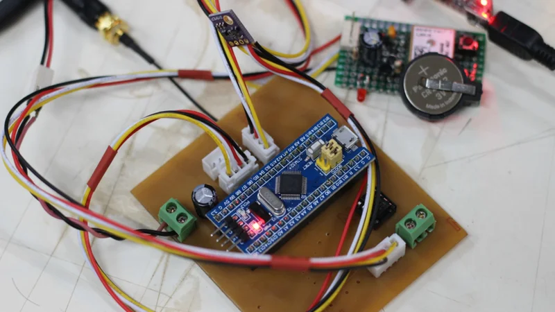
An STM32F103C8T6 Blue Pill wired into a prototype.
Key Takeaways
- The STM32F103 is an Arm Cortex-M3 microcontroller running at up to 72 MHz from a 2.0 to 3.6 V supply, split into four density classes: low, medium, high, and XL.[1][4][16]
- Density and package are both decisions that matter. Density sets flash, SRAM, timer count, and ADC count; package sets how many interfaces are pinned out.[1] One consequence: only high and XL density support dual PMSM field-oriented control in ST's legacy PMSM single/dual FOC SDK (STSW-STM32100, UM1052).[6]
- The STM32F103C8T6 on the Blue Pill is a medium-density part: 64 KB flash, 20 KB SRAM, 37 GPIO, LQFP48, with 2 ADCs sharing 10 external channels, 2 SPI, 2 I2C, 3 USART, 1 USB and 1 CAN.[1]
- USB and CAN share a dedicated 512-byte packet SRAM on this device, so you cannot use both at once.[16] Remapping CAN to PB8/PB9 or PD0/PD1 frees the pins but does not fix it; the buffer is the blocker.[1]
- Two Blue Pill hardware faults matter before you power one up: the +5V pins connect straight to USB +5V with no protection, and the board may carry 10 kΩ or 4.7 kΩ on USB D+ where the spec requires 1.5 kΩ; some hosts enumerate anyway, so measure PA12 to 3.3 V before reworking.[10]
Introduction
The STM32F103 is the part that put STMicroelectronics into low-cost embedded design, and the STM32F103C8T6 on the Blue Pill board is still the cheapest practical route onto Arm Cortex-M3. Boards have been available from China for just under $2.00.[15]
This guide is a reference rather than an introduction to the family. If you want the wider picture of what STM32 is and how the series relate, start with the STM32 microcontroller pillar guide, and use the STM32 family selection guide if you are choosing between series rather than working within this one.
Everything below is drawn from ST's datasheets and reference manual (RM0008), plus the board-level detail ST does not cover.
What the STM32F103 Is
The STM32F103 is a 32-bit Arm Cortex-M3 microcontroller from STMicroelectronics, running at up to 72 MHz from a 2.0 to 3.6 V supply, with 16 KB to 1 MB of flash depending on the part. It is the mainstream line of ST's STM32F1 series, and the STM32F103C8T6 variant is the chip on the Blue Pill board.[1]
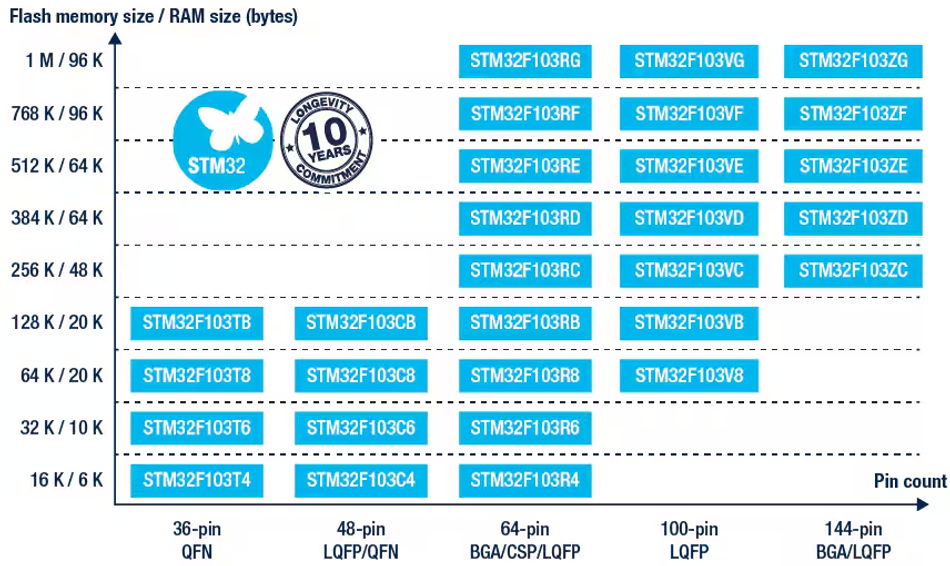
It is a general-purpose part rather than a specialised one. ST targets it at motor drives, industrial control and PLCs, medical and handheld equipment, printers and scanners, GPS, alarm systems and HVAC.[1]
The Cortex-M3 core implements Armv7-M, designed for deeply embedded work: low cycle count execution, minimal interrupt latency, no cache.[9]
Recommended Reading: STM32 Selection Guide: Choosing the Right Part for Your Design
The Four Density Classes
That 16 KB to 1 MB flash span is not one part but four density classes, and they differ in more than memory. It is easy to miss, because every one of them is called STM32F103. ST publishes a separate datasheet for each, and the peripheral set genuinely differs between them.
Density | Parts | Flash | SRAM | Timers | ADCs | Interfaces |
Low | STM32F103x4, x6 | 16 or 32 KB | 6 or 10 KB | 2 general-purpose + 1 advanced-control | 2 | 1 SPI, 1 I2C, 2 USART, USB, CAN |
Medium | STM32F103x8, xB | 64 or 128 KB | up to 20 KB | 3 general-purpose + 1 PWM | 2 | up to 2 I2C, 2 SPI, 3 USART, USB, CAN |
High | STM32F103xC, xD, xE | up to 512 KB | up to 64 KB | Up to 4 general-purpose + 2 PWM | 3 | up to 2 I²C, 3 SPI (SPI2/SPI3 switchable to I²S), 1 SDIO, 5 USART, USB, CAN |
XL | STM32F103xF, xG | 768 Kbytes to 1 MB | 96 KB | Up to 10 general-purpose + 2 PWM | 3 | up to 2 I2C, 3 SPI (SPI2/SPI3 switchable to I²S), 2 I2S, 1 SDIO, 5 USART, USB, CAN |
Sources for the row figures are the corresponding ST datasheets.[1][2][3][4]
Three consequences follow from that table.
I²S, SDIO, and FSMC only exist from high density upward. If your design needs digital audio, an SD card interface, or external memory on the peripheral rather than bit-banged, medium density cannot do it.[3]
The third ADC appears at high density. Low and medium density give you two 12-bit ADCs;[1][2] high and XL give you three.[3][4] Analog output follows the same pattern: high-density parts carry two 12-bit DAC channels, and low- and medium-density parts have none.[3] If you need a DAC, medium density cannot give you one.
Dual motor control needs high or XL density. ST's PMSM FOC software development kit supports "Single or simultaneous Dual PMSM FOC sensorless/sensored," but notes that dual PMSM FOC runs only on STM32F103xx high-density, XL-density, or other families.[6] If you are driving two motors from one STM32F103, medium density is not an option.
Decoding an STM32F103 Order Code
ST publishes the codification in the datasheet itself, and it is worth reading rather than guessing. For medium-density parts the fields are:[1]
Field | Meaning |
STM32 | Arm-based 32-bit microcontroller |
F | Product type: general-purpose |
103 | Device subfamily: performance line |
Pin count | T = 36 pins, C = 48 pins, R = 64 pins, V = 100 pins |
Flash size | 8 = 64 Kbytes, B = 128 Kbytes |
Package | H = BGA, I = UFBGA, T = LQFP, U = VFQFPN or UFQFPN |
Temperature | 6 = industrial, -40 to 85 °C; 7 = industrial, -40 to 105 °C |
Options | Blank for standard product, R for customer-dedicated code, TR for tape and reel, xxx= programmed parts |
So STM32F103C8T6 reads as: performance line, 48 pins, 64 Kbytes of flash, LQFP package, industrial –40 to 85 °C.[1]
One caution. That table is the medium-density codification, so it only lists the pin counts and flash sizes that exist at that density. The letters mean the same thing family-wide, but to decode a part from another density, an STM32F103ZG, say, you need that density's datasheet for the values it adds.[2][3][4] Pin count is the field that does the most work, which the next section unpacks.
Medium-Density Variants and Packages
The C8T6 on the Blue Pill is medium density, so this is the class most readers are actually holding. Within medium density, the pin-count letter drives GPIO count and how many of each interface you get.[1]
All four carry 20 KB of SRAM and are available with either 64 KB or 128 KB of flash.[1]
Two details from that table are easy to trip over. Dropping to the 36-pin VFQFPN costs you one SPI, one I²C, and one USART, not just pins.[1] And on the TFBGA64 package, only 15 ADC channels are available, because one analog input pin has been replaced by VREF+.[1]
Recommended Reading: I2C vs SPI vs UART: A Comprehensive Comparison
Power Supply Pins
The STM32F103 has three main supply domains, and getting the analog one wrong is a common source of poor ADC results.[1] On the 100-pin packages, VREF+ and VREF− are brought out separately as a fourth.[1]
Pin | Range | Purpose |
VDD | 2.0 to 3.6 V | External supply for I/Os and the internal regulator |
VDDA / VSSA | 2.0 to 3.6 V | Analog supply for ADC, reset blocks, RCs, and PLL |
VBAT | 1.8 to 3.6 V | RTC, 32 kHz oscillator, and backup registers when VDD is absent |
The detail worth committing to memory: the minimum voltage to be applied to VDDA is 2.4 V when the ADC is used, even though the part itself runs down to 2.0 V.[1] ST also specifies that VDDA and VSSA must be connected to VDD and VSS respectively, and that a maximum difference of 300 mV between VDD and VDDA can be tolerated during power-up and operation.[1]
The integrated power-on reset and power-down reset circuitry is always active and ensures proper operation from 2 V up to VDD, with no external reset circuit required.[1] NRST is available on every package if you want external reset control, and carries an internal weak pull-up of 30 to 50 kΩ.[1]
Power management beyond that comes from three low-power modes. Sleep stops only the CPU. Stop retains SRAM and register contents. Standby switches off the regulator and loses SRAM and register contents except the backup domain.[1] On a board like the STM32 Blue Pill, budget the regulator's quiescent draw and the power LED alongside the MCU, since on a breakout those are often the dominant loads.
Clocks
The clock tree is where most STM32F103 timing bugs start, because the part does not run at 72 MHz until you configure it to.
On reset, the internal RC 8 MHz oscillator is selected as the default CPU clock.[1] An external 4 to 16 MHz clock can be selected instead, and when it is, it is monitored for failure: if failure is detected, the system automatically switches back to the internal RC oscillator, and a software interrupt is generated if enabled.[1]
This is why the Blue Pill's 8 MHz crystal is not the CPU clock. It is the PLL input, and the PLL is what produces 72 MHz.[10][11] It is also why the crystal is not optional if you want USB: the USB peripheral needs both HSE and PLL running, with USBCLK at 48 MHz.[1]
The prescaler limits catch people out:[1]
AHB and the high-speed APB domain (APB2): maximum 72 MHz
Low-speed APB domain (APB1): maximum 36 MHz
APB1 peripherals such as I²C, SPI2 and USART2/3 run at 36 MHz, half the system clock. Timers are the exception: when the APB1 prescaler is anything other than 1, the timer clock is doubled, so TIM2 to TIM4 are fed at 72 MHz in a standard configuration.[1] Assuming one rule covers both is how baud rates and timer periods end up wrong. Wevolver's guide to crystal oscillator design covers why the external crystal is worth fitting at all.
Boot Modes
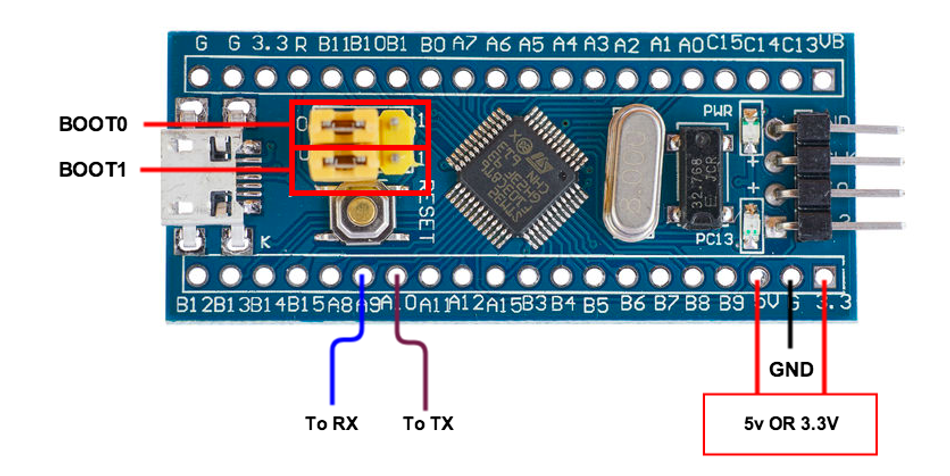
At startup, boot pins select one of three boot options:[1]
- Boot from user flash
- Boot from system memory
- Boot from user flash
The bootloader lives in system memory, and it is used to reprogram the flash memory using USART1.[1] That is the route you take when you have no debugger. ST documents the details in AN2606.[1]
On the LQFP48 package, BOOT0 is a dedicated pin, and BOOT1 is shared with PB2, whose main function after reset is listed as PB2/BOOT1.[1] On the Blue Pill both are brought out to jumpers.[10]
Pinout and Alternate Functions
Most STM32F103 GPIO pins carry several possible functions, and each peripheral is mapped to specific pins rather than to any pin. ST's pin definition table gives, for each pin, a main function after reset, a default alternate function, and in some cases a remapped alternate function.[1]
The I/O Level column marks five-volt-tolerant pins with FT. Most GPIOs carry it, but not all — the datasheet's feature list says almost all I/Os are 5 V-tolerant, and the exceptions are largely the analog-capable pins.[1] Check the column for the specific pin before wiring it to 5 V logic, because the pins that aren't tolerant are the ADC inputs you'd most likely want to feed from a 5 V sensor.
The table below is the LQFP48 subset, which is the package on the Blue Pill. Pins are LQFP48 PINs.[1]
Pin | Name | Default alternate function | Remap |
20 | PB2 | Main function after reset is PB2/BOOT1 | - |
21 | PB10 | I2C2_SCL / USART3_TX | TIM2_CH3 |
22 | PB11 | I2C2_SDA / USART3_RX | TIM2_CH4 |
25 | PB12 | SPI2_NSS / I2C2_SMBA / USART3_CK / TIM1_BKIN | - |
26 | PB13 | SPI2_SCK / USART3_CTS / TIM1_CH1N | - |
27 | PB14 | SPI2_MISO / USART3_RTS / TIM1_CH2N | - |
28 | PB15 | SPI2_MOSI / TIM1_CH3N | - |
29 | PA8 | USART1_CK / TIM1_CH1 / MCO | - |
30 | PA9 | USART1_TX / TIM1_CH2 | - |
31 | PA10 | USART1_RX / TIM1_CH3 | - |
32 | PA11 | USART1_CTS / CANRX / USBDM / TIM1_CH4 | - |
33 | PA12 | USART1_RTS / CANTX / TIM1_ETR / USBDP | - |
34 | PA13 | Main function after reset is JTMS/SWDIO | PA13 |
Note: CAN_RX and CAN_TX can be remapped to PB8/PB9 or PD0/PD1.[1]
The USB and CAN Conflict
PA11 and PA12 carry USBDM/CANRX and USBDP/CANTX, respectively, so by default USB and CAN collide on pins.[1] The pins are the visible half of the problem and the smaller half. CAN can be remapped to PB8/PB9 or PD0/PD1, which clears the collision and still doesn't let you run both: USB and CAN share a dedicated 512-byte SRAM for packet data, and only one peripheral can own it at a time.[16] On this device, you get USB or CAN, never both at once; though you can use each in the same application at different times. The constraint is invisible in the pin table, which is why it catches people who have already tried remapping.
Recommended Reading: Understanding CAN Bus: A Comprehensive Guide
Debug Pins are Alive from Reset
PA13's main function after reset is JTMS/SWDIO, not general-purpose I/O.[1] The debug port is active before your code configures anything, which is what makes SWD recovery possible on a board with no bootloader. It also means you should not casually reuse PA13 and PA14 as GPIO unless you are willing to lose your debugger.
The same applies to PA15, PB3 and PB4, which come up as JTDI, JTDO and NJTRST.[1] Those three catch people out more often, because they look like ordinary GPIO in a pinout diagram and only free up once you switch to SWD or disable the JTAG port in AFIO.
The STM32F103C8T6 Blue Pill Board
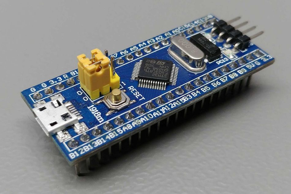
The Blue Pill is a minimal breakout: the STM32F103C8T6, a regulator, footprints for two crystals, a USB connector, and headers.
Item | Specification |
MCU | STM32F103C8T6, Arm Cortex-M3 at 72 MHz |
Memory | 64 KB flash, 20 KB SRAM |
Board size | 23 mm x 53 mm |
Regulator | +3.3 V at 300 mA |
High-speed oscillator | 8 MHz HSE |
Low-speed oscillator | 32.768 kHz LSE |
Debug header | VCC, SWDIO (PA13), SWCLK (PA14), GND |
Board-level figures are from the STM32-base project's reference, since ST does not document third-party boards.[10]
Two Hardware Faults to Know Before you Power it
The +5V pins have no protection. The +5V pins connect directly to the +5V pin of the USB connector, with no protection in place.[10] The accompanying warning follows: do not power the board through USB and an external power supply at the same time.[10]
The USB D+ pull-up may be the wrong value. The board "may have a wrong value of resistor on the USB D+ pin. Instead of a 1.5kΩ, it has either a 10kΩ or 4.7kΩ resistor."[10] A pull-up outside the specified value is the usual explanation offered for boards that fail to enumerate, and the fixes commonly discussed are replacing the resistor or adding a correct one in parallel. Treat that diagnosis and remedy as community practice rather than a manufacturer instruction.
Worth knowing alongside it: as shipped these boards carry no USB bootloader in flash. You can flash a USB bootloader using OpenOCD or the serial loader, then use USB for subsequent loading.[15]
Programming and Debug
You have three practical routes onto an STM32F103, and they are not equally good.
SWD with an ST-LINK. The Blue Pill exposes a four-pin debug header: VCC, SWDIO on PA13, SWCLK on PA14, GND.[10] This is the only route that also gives you breakpoints, single-stepping, and register visibility. One practitioner's summary is representative: use "OpenOCD and a ST-Link V2 to load my software via the SWD interface."[15]
The built-in serial bootloader is selected with the boot pins and driven over USART1.[1] ST documents the protocol in AN2606.[1]
USB DFU, which requires flashing a USB bootloader first, since the bare board ships without one.[15]
Arduino and HAL options
If you want the Arduino toolchain, the official core is STM32duino. It "adds the support of STM32 MCU in Arduino IDE 2.x" and is built on ST's own STM32Cube MCU packages: the HAL hardware abstraction layer, the Low-Layer (LL) APIs, and the CMSIS device definitions.[12] It supports generic boards across the STM32F1 series among many others.[12]
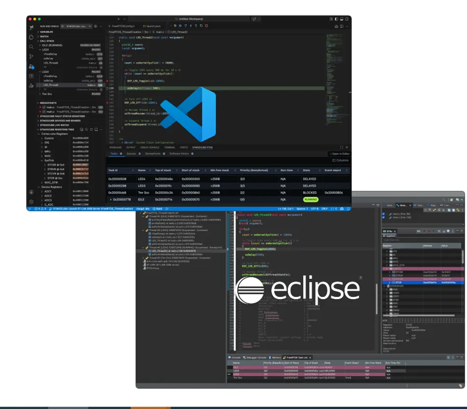
Arduino sketches on this part therefore run on ST's HAL underneath, so dropping to LL or to direct register access later does not mean abandoning your toolchain. If you are coming from an 8-bit background, Wevolver's Arduino Uno pinout guide is a useful comparison point.
Zephyr is another option, and its board definition for an STM32F103RC-based board gives a concrete default mapping: USART1 on PA9 and PA10, SPI1 on PA4 to PA7, I2C1 on PB9 and PB8, timer 1 channel 1 PWM on PA8, and USB on PA11 and PA12.[11] Those match ST's default alternate functions for the same pins, with one exception: I2C1's default position is PB6 and PB7, and PB8/PB9 is the remap.[1]
Recommended Reading: What Is a PWM Signal? Fundamentals and Practical Applications for Engineers
USB on the F103
The STM32F103 embeds a USB device peripheral compatible with USB full-speed, 12 Mbit/s, implementing a full-speed function interface.[1] It is device-only, so you cannot make this part a USB host.[1]
The USB subsystem needs a 48 MHz clock, generated from the internal main PLL, and the clock source must use an HSE crystal oscillator.[1] That is why the crystal and PLL configuration matter. if you intend to use USB communication at all, that is another reason the internal RC oscillator alone is not sufficient for USB work.
Clone and Counterfeit Chips
This is the most expensive trap on cheap boards, and it is well documented.
Several manufacturers produce STM32F103 workalikes. The CS32F103 comes from CKS, a Chinese company that has produced what appears to be a feature-complete version of the part. The GD32F103 from GigaDevice is faster and more capable, running at 108 MHz against the STM32F103's 72 MHz, and uses a separate flash die over SPI with SRAM caching rather than on-die flash. The CH32F103C8T6 comes from WCH.[14]
Not all of these are the same thing. A GD32 or CS32 sold as a GD32 or CS32 is a legitimate compatible part. The problem is remarked chips sold as genuine ST silicon, and outright forgeries: STM32FEBKC6 is "not a legitimate ST parts code."[14]
How to Identify One
Method | What to look for |
CPU TAP ID | Genuine reports 0x1ba01477. CS32F103 and CH32F103 report 0x2ba01477.[14] |
Erratum behavior | CS32F103 "fixes Erratum 2.3 of genuine STM32F103" on debug register return values, so behaving correctly here identifies a clone. This assumes the erratum is still unfixed in the genuine silicon revision you are comparing against. [13] |
Package marking | Compare against ST's own reference marking schematics, which define the pin 1 identifier, product identification, date code, and revision code areas.[5] |
The TAP ID check is the practical one, since you see it the moment you connect OpenOCD or an ST-LINK.
On marking, ST publishes TN1433, a reference document of device marking schematics covering STM32 microcontrollers and microprocessors.[5] It gives you an authoritative baseline to compare a suspect part against, which is more useful than judging silkscreen quality by eye. ST does note that marking varies slightly between assembly plants, so only the pin 1 identifier location is invariant.[5] The document also flags parts marked "ES" or "E" as engineering samples, not qualified and not approved for production use.[5]
What Goes Wrong with Fakes
A project maintainer documented these specific faults on a fake STM32F103C8: it cannot program at 921600 baud though it succeeds at 115200, it cannot start firmware from the System Bootloader, writing to backup registers appears to lock up parts of the chip, the I2C peripheral will not allow CR1_ACK to be set in the same write that sets CR1_PE, and the "DMA peripheral generates spurious extra completion interrupts and is generally prone to lockup."[13]
Those are the kind of faults that cost days, because the board mostly works. Clones run basic blink firmware without trouble.[14] The failure appears later, in DMA or I2C, and looks like a firmware bug.
Common Mistakes
Assuming all STM32F103 parts are alike. Density class changes the peripheral set, not just memory size. I2S, SDIO, DAC and FSMC do not exist below high density.[1][3]
Trying to use USB and CAN together. They share a dedicated 512-byte packet SRAM, and remapping CAN off PA11/PA12 doesn't help.[16]
Running the ADC with VDDA below 2.4 V. The device runs to 2.0 V, but the ADC needs VDDA at 2.4 V minimum.[1]
Forgetting APB1 is capped at 36 MHz. The system clock reaches 72 MHz, the low-speed APB domain does not.[1]
Powering from USB and an external supply together. The +5V rail has no protection on the Blue Pill.[10]
Buying the cheapest board for production. Remarked chips are reported at the bottom of the market, with the CS32F103 said to turn up remarked as genuine STM32F103 silicon.[13] Prototyping on a two-dollar board is fine. Shipping on one is a supply-chain decision to make deliberately.
Conclusion
The STM32F103 remains a sensible reference point for Cortex-M3 work: predictable, cacheless, thoroughly documented, and cheap enough to buy several. Two things separate people who get on with it from people who lose a week. The first is reading the density class rather than the family name. The second is reading past the pin table: the USB and CAN conflict lives in a shared buffer, not in the pins, and the debug pin assignments are not obvious from a board silkscreen.
If you are working with a board you already have, check the TAP ID before you trust it. If you are choosing between STM32 series rather than within this one, the family selection guide covers the newer lines.
Frequently Asked Questions
How much flash and RAM does the STM32F103C8T6 have?
The STM32F103C8T6 has 64 KB of flash and 20 KB of SRAM.[1] It is a medium-density part in an LQFP48 package with 37 GPIO, 2 ADCs, 2 SPI, 2 I²C, 3 USART, 1 USB and 1 CAN.[1]
What is the difference between the STM32F103C8T6 and the STM32F103CBT6?
Flash size only. In ST's order code, 8 means 64 Kbytes and B means 128 Kbytes.[1] Both are medium-density parts with 20 KB of SRAM, the same peripheral set, and the same LQFP48 package.[1]
Can the STM32F103 use USB and CAN at the same time?
No. USB and CAN share a dedicated 512-byte packet SRAM on the STM32F103, and only one peripheral can own it at a time. The two also collide on pins PA11 and PA12 by default, but remapping CAN to PB8/PB9 or PD0/PD1 frees the pins without solving the conflict.[1] Both can be used in the same application, just not simultaneously.
What does the 6 at the end of STM32F103C8T6 mean?
The 6 is the temperature range: industrial, –40 to 85 °C.[1] A 7 in that position means industrial, –40 to 105 °C. Reading the code backwards from there, T means an LQFP package, 8 means 64 Kbytes of flash, and C means 48 pins.[1]
Which STM32F103 supports SDIO or I2S?
Only high-density and XL-density STM32F103 parts. High density adds SDIO, I²S, DAC and FSMC, none of which exist on low- or medium-density devices.[1][3] High-density parts are the STM32F103xC, xD and xE; XL density is the xF and xG, which carry one SDIO and two I²S interfaces along with an MPU and dual-bank flash.[4]
How do I program a Blue Pill without a USB bootloader?
Use SWD with an ST-LINK on the four-pin debug header: VCC, SWDIO on PA13, SWCLK on PA14, GND.[10] The alternative is the bootloader in system memory, selected with the boot pins, which reprograms flash over USART1.[1]
Is the STM32F103 5 V tolerant?
Partly. Most general-purpose I/O pins are five-volt tolerant, marked FT in the I/O Level column of ST's pin definition table, but the analog-capable pins are not; PA0 to PA7, PB0, PB1, PB5 and PC0 to PC5 have no FT marking.[1] The supply itself is 2.0 to 3.6 V, so the STM32F103 is not a 5 V device. Check the level marking for each pin you intend to drive.[1]
How can I tell if my STM32F103 is genuine?
Check the CPU TAP ID when you connect a debugger. Genuine ST parts report 0x1ba01477, while CS32F103 and CH32F103 clones report 0x2ba01477.[14] A matching ID is not proof of a genuine part, though, it rules out those two clones and nothing more, since other workalikes report the same value as ST silicon. For package marking, compare against ST's reference marking schematics in TN1433, bearing in mind that ST notes marking varies slightly between assembly plants, so only the pin 1 identifier location is invariant.[5]
References
[1] STMicroelectronics, "STM32F103x8, STM32F103xB: Medium-density performance line Arm-based 32-bit MCU with 64 or 128 KB flash, USB, CAN, seven timers, two ADCs, nine communication interfaces," datasheet DS5319 Rev. 20, Jul. 2025. [Online]. Available: https://www.st.com/resource/en/datasheet/stm32f103c8.pdf
[2] STMicroelectronics, "STM32F103x4, STM32F103x6: Low-density performance line Arm-based 32-bit MCU with 16 or 32 KB flash, USB, CAN, six timers, two ADCs, six communication interfaces," datasheet DocID15060 Rev. 7, Jun. 2015. [Online]. Available: https://www.st.com/resource/en/datasheet/stm32f103c4.pdf
[3] STMicroelectronics, "STM32F103xC, STM32F103xD, STM32F103xE: High-density performance line Arm-based 32-bit MCU with 256 to 512 KB flash, USB, CAN, 11 timers, three ADCs, 13 communication interfaces," datasheet DS5792 Rev. 13, Jul. 2018. [Online]. Available: https://www.st.com/resource/en/datasheet/stm32f103rc.pdf
[4] STMicroelectronics, "STM32F103xF, STM32F103xG: XL-density performance line Arm-based 32-bit MCU," datasheet DocID16554 Rev. 4, May 2015. [Online]. Available: https://www.st.com/resource/en/datasheet/stm32f103rf.pdf
[5] STMicroelectronics, "Reference device marking schematics for STM32 microcontrollers and microprocessors," technical note TN1433 Rev. 7, Dec. 2025.
[6] STMicroelectronics, "STM32F PMSM single/dual FOC SDK v4.3," user manual UM1052. [Online]. Available: https://www.st.com/resource/en/user_manual/um1052-stm32f-pmsm-singledual-foc-sdk-v43-stmicroelectronics.pdf
[7] STMicroelectronics. "STM32F103." Accessed: Sep. 16, 2026. [Online]. Available: https://www.st.com/en/microcontrollers-microprocessors/stm32f103.html
[8] STMicroelectronics. "STM32F103 product selector." Accessed: Sep. 16, 2026. [Online]. Available: https://www.st.com/en/microcontrollers-microprocessors/stm32f103/products.html
[9] Arm Ltd. "Cortex-M3." Accessed: Sep. 16, 2026. [Online]. Available: https://www.arm.com/products/silicon-ip-cpu/cortex-m/cortex-m3
[10] STM32-base project. "STM32F103C8T6 Blue Pill." Accessed: Sep. 16, 2026. [Online]. Available: https://stm32-base.org/boards/STM32F103C8T6-Blue-Pill.html
[11] Zephyr Project. "STM32F103 Mini." Accessed: Sep. 16, 2026. [Online]. Available: https://docs.zephyrproject.org/latest/boards/others/stm32f103_mini/doc/index.html
[12] STM32duino. "Arduino Core STM32." GitHub. Accessed: Sep. 16, 2026. [Online]. Available: https://github.com/stm32duino/Arduino_Core_STM32
[13] K. Fraser. "STM32 fakes." Greaseweazle wiki, GitHub. Accessed: Sep. 16, 2026. [Online]. Available: https://github.com/keirf/greaseweazle/wiki/STM32-Fakes
[14] M. Posch. "STM32 clones: The good, the bad and the ugly." Hackaday, Oct. 22, 2020. Accessed: Sep. 16, 2026. [Online]. Available: https://hackaday.com/2020/10/22/stm32-clones-the-good-the-bad-and-the-ugly/
[15] T. Trebisky. "The STM32F103C8T6 and USB." MMT Observatory, Oct. 29, 2023. Accessed: Sep. 16, 2026. [Online]. Available: http://kofa.mmto.arizona.edu/stm32/blue_pill/usb/
[16] STMicroelectronics, "STM32F101xx, STM32F102xx, STM32F103xx, STM32F105xx and STM32F107xx advanced Arm-based 32-bit MCUs," reference manual RM0008.
in this article
1. Key Takeaways2. Introduction3. What the STM32F103 Is4. The Four Density Classes5. Decoding an STM32F103 Order Code6. Medium-Density Variants and Packages7. Power Supply Pins8. Clocks9. Boot Modes10. Pinout and Alternate Functions11. The STM32F103C8T6 Blue Pill Board12. Programming and Debug13. Arduino and HAL options14. USB on the F10315. Clone and Counterfeit Chips16. Common Mistakes17. Conclusion18. Frequently Asked Questions19. References