Silicon Wafers: Production, Properties and Application
Silicon wafers are thin slices of highly pure crystalline Silicon, used in the production of integrated circuits. This article delves into the fascinating world of silicon wafers, unraveling their production process, unique properties, and the wide range of applications that make them indispensable.

Last updated on 11 Jan, 2024. 16 minutes read
Wafers
Introduction
Silicon wafers are a fundamental component in the technology industry, serving as the substrate material for microelectronic devices. These thin slices of semiconductor material form the basis for integrated circuits (ICs), which are used in a wide range of electronic devices, from smartphones and computers to advanced medical equipment and aerospace technology. Silicon, a crucial semiconductor, dominates the electronic and technology sector due to its conductivity and affordability. Silicon ranks seventh in universal abundance and second on Earth. Common silicon-containing materials include beach sand, quartz, and flint.
While silicon crystals resemble metals, they are not actual metals. Pure silicon crystals act as insulators, allowing minimal electricity flow, but this changes through doping. Doping is when a little amount of an impurity is mixed into a silicon crystal to change its behavior and integrate it into a conductor. These impurities used for doping are called dopants. Silicon (Si) by itself does not conduct electricity very well; however, it can take on dopants precisely to control resistivity to an exact specification. Measured in ohm-centimeters ( ohm-cm or Ω⋅cm), resistivity quantifies how effectively the material conducts or resists the flow of electrical current. Silicon (Si) dopants such as nitrogen, indium, aluminum, gallium, and boron can be added throughout the growing process. So, for a semiconductor to be formed out of the non-conductive silicon, silicon must turn into a wafer; hence, a silicon wafer.
Silicon wafers, available in various shapes and sizes, are integral to integrated circuits, playing a vital role in electronic devices. These wafers undergo fabrication methods such as Vertical Bridgeman, Czochralski pulling, and the emerging Float Zone, known for fewer defects and superior purity. Silicon wafers are widely employed in chip and microchip manufacturing for electronic devices. The miniaturization of electronic components, made possible by the use of silicon wafers, has led to the development of increasingly compact and powerful devices. This has opened up new possibilities in communication, data processing, and automation, among other areas. The production of silicon wafers is a complex and precise process. It involves the transformation of raw silicon into a highly pure, single-crystal substrate. This process requires advanced technology and stringent quality control to ensure the production of high-quality wafers that meet the exacting standards of the tech industry.[1]
The Manufacturing Process of Silicon Wafers
The production of silicon wafers is a multi-step process that begins with the extraction of raw silicon from quartz. Silicon (Si) is the second most abundant element on Earth, but it is not found in its pure form. Instead, it is typically found in the form of silicon dioxide (SiO2) or quartz. The extraction process involves heating the quartz in a high-temperature furnace in the presence of carbon, which reduces the silicon dioxide to silicon.
Once the raw silicon has been extracted, it must be purified to a high degree. This is because the performance of electronic devices is highly sensitive to impurities in the silicon substrate. The purification process involves several steps, including refining, zone melting, and solidification, which collectively increase the purity of the silicon to 99.9999% or higher. It is then allowed to solidify into a silicon rod, or ingot, by using common fabrication methods like the Floating Zone or Czochralski process. Czochralski's method involves the placement of a small piece of solid silicon in a pool of molten silicon, and then pulled slowly in rotation as the liquid transforms into a cylindrical ingot.
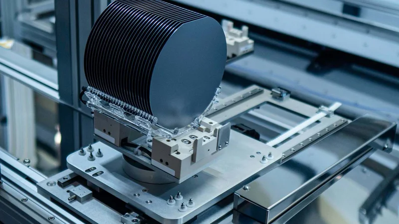
This is why the end product wafers are all disc-shaped. Before it cools off completely, the pyramidal ends of the ingot are yanked off. Sharp diamond saw blades are then used to slice the body into thin wafers of the same thickness. This clarifies why the diameter of an ingot would be the determinant of a wafer size. The wafers are typically around 1 millimeter thick, but can be made thinner for certain applications. After slicing, the wafers are polished to create a smooth, flat surface that is suitable for the fabrication of electronic devices.[2]
The Czochralski Process
The Czochralski process is a method of crystal growth used to obtain single crystals of semiconductors, metals, salts and synthetic gemstones. Named after Polish scientist Jan Czochralski, who invented the method in 1916, it is used to produce single crystal silicon used for semiconductor devices. The process begins with a seed crystal being dipped into a crucible containing molten silicon. The seed crystal, which is attached to a rod, is slowly pulled upwards and rotated simultaneously.
As the seed crystal is lifted, the molten silicon cools and solidifies, maintaining the crystal structure of the seed. The rate at which the seed crystal is lifted and the temperature of the environment are carefully controlled to ensure a uniform crystal structure. The result is a large, cylindrical crystal of silicon, known as a boule. The boule is then sliced into thin wafers, which are subsequently polished and used in semiconductor manufacturing. The Czochralski process is renowned for producing high-quality crystals with few defects, making it the preferred method for producing silicon wafers in the semiconductor industry.[3]
Wafer Slicing and Polishing
After the formation of the silicon boule through the Czochralski process, the next step in the production of silicon wafers is slicing and polishing. The boule, a cylindrical single crystal of silicon, is sliced into thin discs, or wafers, using a diamond saw. The diamond saw is used due to its hardness, which allows for precise and clean cuts. The thickness of the wafer surface depends on the specific requirements of the semiconductor devices they will be used to produce, but they are typically around 1 millimeter thick. The slicing process must be carefully controlled to ensure the wafers are of uniform thickness and free from defects. Any irregularities in the wafer can impact the performance of the semiconductor devices they are used to produce. Therefore, the slicing process is a critical step in the production of silicon wafers.
After the wafers have been sliced, they undergo a series of cleaning and polishing steps to prepare them for the fabrication of electronic devices. The first step is a cleaning process that removes any residual silicon dust from the slicing process. This is typically done using a combination of chemicals and ultrasonic agitation. Following the cleaning process, the wafers are polished to create a smooth, flat surface. The polishing process involves the use of a polishing slurry, which is a mixture of chemicals and abrasive particles. The wafers are polished on both sides to ensure a uniform surface.
The polishing process not only improves the physical appearance of the wafers but also enhances their electrical properties. A smooth, flat surface is essential for the subsequent deposition of thin films or layers of other materials during the fabrication of semiconductor devices. Therefore, the slicing and polishing processes are critical steps in the production of high-quality silicon wafers.[4]
Thin Films in Silicon Wafers
Thin Films are layer or coating of material that is deposited onto the surface of the silicon wafer. These thin films can serve various purposes and are crucial for the fabrication of semiconductor devices. The deposition of thin films is a key step in the manufacturing process, and it involves applying a layer of material onto the wafer to achieve specific properties or functions.
Here are a few common types of thin films used in silicon wafer technology:
Dielectric Thin Films: These films are insulating layers that help isolate different components of a semiconductor device. Silicon dioxide (SiO2) is a common dielectric thin film used for this purpose.
Metal Thin Films: Metals like aluminum or copper are often deposited as thin films to create conductive paths or interconnects between different parts of the semiconductor device.
Semiconductor Thin Films: In some cases, additional semiconductor materials are deposited as thin films to modify the electrical properties of the silicon wafer.
Passivation Films: Thin films are sometimes applied to protect the surface of the silicon wafer and improve the overall device performance. Silicon nitride (Si3N4) is an example of a passivation thin film.
The deposition of these thin films is typically done using techniques such as chemical vapor deposition (CVD), physical vapor deposition (PVD), or atomic layer deposition (ALD). The choice of thin film materials and deposition methods depends on the specific requirements of the semiconductor device being manufactured.[5]
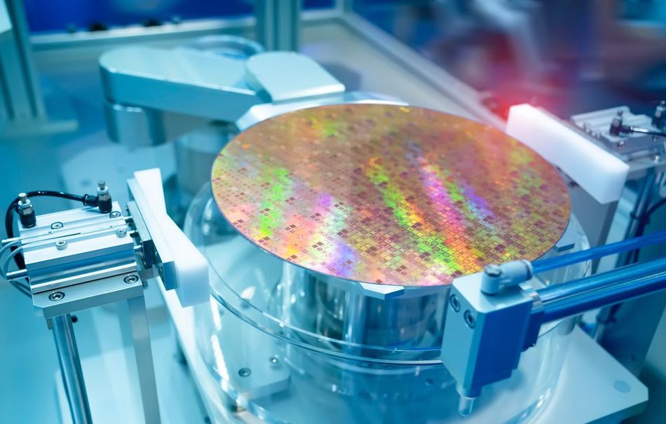
Below are the names and functions of each component of a completed wafer.
1. Edge Die(chips): It is considered as the production loss. The chips along the edge of a wafer. Larger wafers have less chip loss.
2. Scribe Lines: Between the functional portions, there are narrow, non-functional areas where a saw can securely cut the wafer without destroying the circuits. These thin areas are the scribe lines
3. Chip: a little piece of silicon that has electronic circuit patterns
4. Flat Zone: edge of a wafer that is yanked off flat to aid in wafer orientation and type identification.
5. Test Element Group (TEG): a prototype pattern that displays the actual physical features of a chip (diodes, circuits, capacitors, transistors, and resistors) so that it may be tested to know if it works adequately.
Further reading: Wafer Thinning: Investigating an essential part of semiconductor fabrication
Properties of Silicon Wafers
Silicon wafers possess a unique combination of physical and chemical properties that make them ideal for use in the technology industry. These properties include electrical conductivity, thermal conductivity, and mechanical strength, among others. Understanding these properties is essential for the design and fabrication of electronic devices, as they directly impact the performance and reliability of the devices.[6]
Electrical Properties
One of the most important properties of silicon wafers is their electrical conductivity. Silicon is a semiconductor, which means that its electrical conductivity lies between that of a conductor, like copper, and an insulator, like glass. The electrical properties of silicon can be precisely controlled by introducing small amounts of impurities, a process known as doping.
Doping involves the addition of either electron-donating elements, such as phosphorus or arsenic, or electron-accepting elements, such as boron or aluminum. The introduction of these impurities creates either an excess or a deficiency of electrons in the silicon lattice, resulting in either n-type or p-type silicon, respectively. The controlled introduction of these impurities allows for the creation of specific electrical properties in the silicon wafer, which is essential for the fabrication of semiconductor devices.
The ability to control the electrical properties of silicon wafers is crucial for the development of electronic devices, such as transistors, diodes, and integrated circuits. These devices rely on the precise control of electrical current flow, which is made possible by the unique electrical properties of silicon wafers. The performance, efficiency, and reliability of electronic devices are directly influenced by the quality and consistency of the silicon wafers used in their fabrication.
Thermal Properties
Silicon wafers also exhibit unique thermal properties that are critical to their function in electronic devices. One of the key thermal properties of silicon is its thermal conductivity, which is the measure of a material's ability to conduct heat. Silicon has a relatively high thermal conductivity, around 149 W/m·K at room temperature. This property is crucial in electronic devices, as it allows for the efficient dissipation of heat generated during operation, thereby preventing overheating and ensuring the reliability and longevity of the device.
Another important thermal property of silicon is its coefficient of thermal expansion (CTE), which measures how much the material expands or contracts with changes in temperature. Silicon has a relatively low CTE, around 2.6 µm/(m·K) at room temperature. This means that silicon wafers do not significantly expand or contract with temperature changes, which is important in the fabrication and operation of electronic devices. Large changes in dimension with temperature can lead to mechanical stresses and potential failure of the device.
The thermal properties of silicon wafers are not only important for the operation of the devices they are used to produce, but also for the fabrication process itself. Many steps in the fabrication process, such as doping and oxide growth, involve high temperatures. The high thermal conductivity and low CTE of silicon wafers allow these processes to be carried out efficiently and without inducing mechanical stresses in the wafer.
Applications of Silicon Wafers
Silicon wafers are used in a wide range of applications within the technology industry, thanks to their unique combination of electrical and thermal properties. These applications include the fabrication of semiconductor devices, solar cells, and other electronic components. The versatility of silicon wafers has made them an essential material in the development of modern technology.
In the Semiconductor Industry with MEMS Integration
Silicon wafers play a pivotal role in the semiconductor industry, serving as the foundation for the production of integrated circuits (ICs) and various semiconductor devices. These ICs, essential for modern electronics, enable the compact design and enhanced functionality of devices like smartphones, computers, and medical equipment.
In semiconductor manufacturing, silicon wafers serve as the canvas for depositing thin films or layers of diverse materials. Through subsequent processes of photolithography, etching, and doping, these layers are transformed into the desired electronic components. The paramount importance of high purity and precise electrical properties in silicon wafers is evident, as even minor impurities or variations can lead to operational failures.
Furthermore, silicon wafers are integral to the manufacturing of discrete semiconductor devices, such as transistors and diodes. These devices, fundamental to electronic circuits, govern the flow of electrical current and facilitate functions like amplification, switching, and rectification of electrical signals. Beyond their unique electrical properties, silicon wafers, with their high thermal conductivity and low coefficient of thermal expansion, emerge as an ideal material for crafting these essential electronic components.
The integration of MEMS technology further elevates the capabilities of silicon wafers, expanding their applications in diverse technological realms. MEMS, or Micro-Electro-Mechanical Systems, bring a new dimension to semiconductor devices by incorporating tiny sensors, actuators, and other microstructures directly onto silicon wafers. This integration enhances the precision, responsiveness, and versatility of semiconductor devices, contributing to advancements in various technological fields.[7]
Further reading: Silicon Semiconductor: A Comprehensive Guide to Silicon and its Use in Semiconductor Technology
In Solar Cells
Silicon wafers play a crucial role in the production of solar cells, which are the key components of solar panels used for harnessing solar energy. Solar cells, also known as photovoltaic cells, convert sunlight directly into electricity through the photovoltaic effect. This process involves the generation of a flow of electricity in a material upon exposure to light. The majority of solar cells are made from silicon due to its excellent semiconductor properties. Silicon's ability to absorb sunlight and its semiconductor nature makes it an ideal material for solar cells. When sunlight hits the silicon wafer in a solar cell, it excites the electrons, causing them to move and create an electric current.
There are two main types of silicon used in solar cells: monocrystalline and polycrystalline silicon. Monocrystalline silicon is made from a single crystal structure, which allows for the free and unimpeded flow of electrons, resulting in high efficiency. Polycrystalline silicon, on the other hand, is made from multiple crystal structures, which can impede the flow of electrons and result in lower efficiency, but it is cheaper to produce.
The production of silicon wafers for solar cells involves similar processes to those used in the semiconductor industry, including the Czochralski process, wafer slicing, and polishing. However, the wafers used in solar cells are typically thicker and less pure than those used in the semiconductor industry. Despite these differences, the fundamental properties of silicon wafers, including their electrical and thermal properties, make them an essential component in the production of solar cells.[8]

Alternative to Silicon Wafer
Although, silicon carbide (SiC) is not a part of the silicon wafer, it is a distinct material that can be used as an alternative to traditional silicon wafers in certain applications. Silicon carbide is a compound made up of silicon and carbon, and it has unique properties that make it advantageous for specific uses in the semiconductor industry.
Silicon carbide wafers can be used in place of silicon wafers in the fabrication of electronic devices. Silicon carbide (SiC) has excellent thermal conductivity, high breakdown voltage, and can operate at higher temperatures compared to silicon. These properties make SiC suitable for high-power and high-frequency electronic applications, such as power devices in electric vehicles, radio-frequency (RF) devices, and high-temperature applications.
However, it's important to note that SiC wafers are a specific subset, and silicon wafers, primarily made from crystalline silicon, remain the standard in many semiconductor applications.
Challenges and Solutions in Silicon Wafer Production
The production of silicon wafers involves a series of complex processes, each of which presents its own set of challenges. These challenges range from maintaining the purity of the silicon during the manufacturing process to managing the high costs associated with the production of high-quality silicon wafers. Despite these challenges, solutions have been developed that allow for the efficient and cost-effective production of silicon wafers.[9]
Maintaining Purity
One of the primary challenges in silicon wafer manufacturing is maintaining the purity of the silicon throughout the manufacturing process. The electrical properties of silicon wafers, which are critical to their function in electronic devices, are highly sensitive to impurities. Even trace amounts of impurities can significantly alter these properties, leading to device failure.
To address this challenge, the production of silicon wafers begins with the creation of ultra-pure silicon through a process known as the Siemens process. This process involves the reaction of hydrogen with trichlorosilane, a silicon compound, at high temperatures to produce ultra-pure silicon. The resulting silicon is then further purified through the Czochralski process, which involves the growth of a single crystal of silicon from a molten pool of ultra-pure silicon.
Despite these purification processes, maintaining the purity of the silicon during the subsequent wafer slicing and polishing processes can be challenging. These processes can introduce impurities into the silicon, which can alter its electrical properties. To prevent this, the slicing and polishing processes are carried out in cleanroom environments, where the level of airborne particles is strictly controlled.
In addition, the wafers are cleaned after slicing to remove any residual silicon dust, which can also introduce impurities. The cleaning process typically involves a combination of chemicals and ultrasonic agitation, which effectively removes the silicon dust without introducing additional impurities. Despite the challenges associated with maintaining the purity of silicon wafers, the solutions developed to address these challenges have enabled the production of high-quality silicon wafers with the precise electrical properties required for the fabrication of electronic devices.
Reducing Production Costs
Another significant challenge in silicon wafer manufacturing is the high cost associated with the process. The production of silicon wafers involves several complex and energy-intensive processes, including the Siemens process for creating ultra-pure silicon, the Czochralski process for growing single silicon crystals, and the wafer slicing and polishing processes. Each of these processes requires specialized equipment and a significant amount of energy, contributing to the high cost of silicon wafer manufacturing.
One approach to reducing production costs is through process optimization. This involves the careful analysis and improvement of each step in the manufacturing process to increase efficiency and reduce waste. For example, the Czochralski process can be optimized by carefully controlling the temperature and pulling rate to maximize the size of the silicon crystal that can be grown from a single batch of molten silicon. Similarly, the wafer slicing process can be optimized by using advanced slicing techniques, such as wire saw slicing, which can produce thinner wafers and thus more wafers per silicon ingot.
Another approach to reducing production costs is through the recycling of silicon waste. During the wafer slicing and polishing processes, a significant amount of silicon is lost as waste. This silicon waste can be collected and recycled back into the manufacturing process, reducing the amount of new silicon that needs to be produced.
The use of alternative materials for certain applications can also help to reduce production costs. For example, for applications that do not require the high purity and precise electrical properties of silicon, other less expensive materials, such as glass or plastic, can be used.
Despite the high costs associated with silicon wafer production, the development of cost-reducing strategies, such as process optimization, silicon recycling, and the use of alternative materials, has enabled the production of silicon wafers to remain economically viable. These strategies, combined with the ongoing demand for silicon wafers in the technology industry, ensure the continued production and use of this essential material.
Conclusion
Silicon wafers play an indispensable role in numerous aspects of human life and technological progress, renowned for their stability among semiconductor materials. These wafers are not only a superior alternative to metallic substances but also widely available on Earth. Research on semiconductor materials like silicon, silicon carbide (SiC), germanium, arsenide, and gallium has propelled significant technological advancements. The invention of ICs, powered by silicon wafers, has revolutionized manufacturing, transforming large machinery into portable devices. Ongoing research focuses on expanding wafer size and controlling properties through doping, promising more sophisticated inventions from silicon wafers in the near future.
As a fundamental component in the technology industry, silicon wafers serve as the foundation for integrated circuits, semiconductor devices, and solar cells. Renowned for their unique electrical and thermal properties, coupled with high purity, these wafers are crucial for various applications. Despite challenges in production, efficient and cost-effective solutions have been devised, ensuring the sustained availability of this crucial material for the technology industry through continuous advancements in production technology.
Frequently Asked Questions
1. What are silicon wafers?
Silicon wafers are thin slices of silicon that serve as the substrate for the fabrication of electronic devices. They are produced from ultra-pure silicon through a series of complex processes, including the Czochralski process, wafer slicing, and polishing.
2. Why are silicon wafers used in the technology industry?
Silicon wafers are used in the technology industry due to their unique electrical and thermal properties. These properties, combined with the high purity of silicon, make it an ideal material for integrated circuits and other semiconductor manufacturing, as well as solar cells.
3. What are the challenges in silicon wafer manufacturing?
The production of silicon wafers involves several challenges, including maintaining the purity of the silicon throughout the production process and managing the high costs associated with the process. Solutions have been developed to address these challenges, including process optimization, silicon recycling, and the use of alternative materials.
4. What is the future of silicon wafer production?
The future of silicon wafer production is likely to involve further advancements in production technology, aimed at increasing efficiency, reducing costs, and improving the quality of the wafers. These advancements, combined with the ongoing demand for silicon wafers in the technology industry, ensure the continued production and use of this essential material.
References
1. Pappas, S. (2018) Facts about Silicon. Available at: https://www.livescience.com/28893-silicon.html
2. SVM (na). The Silicon Wafer Manufacturing Process. Available at: https://svmi.com/service/silicon-wafer-manufacturing-process/
3. The Czochralski Process. Available at: https://www.pvatepla-cgs.com/en/technologies/czochralski-process-cz/
4. SUMCO, 2017. Wafer Forming Process. Available at: https://www.sumcosi.com/english/products/process/step_02.html
5. ScienceDirect, 2017. Silicon Wafer and Thin Film Measurements. Available at: https://www.sciencedirect.com/science/article/pii/B9780323299657000154
6. Semiconductor Nanotechnology: Advances in Information and Energy Processing and Storage - Nanostructure Science and Technology. Stephen M. Goodnick (editor), Anatoli Korkin (editor), Robert Nemanich (editor), Springer Nature Switzerland AG 2018
7. Wafers World Incorporated (2016). What is it and What is it used for? Available at: https://www.waferworld.com/post/silicon-wafer-what-is-it-and-what-is-it-used-for
8. AZO Materials. Silicon in Electronic Devices and Solar Cell Applications. Available at: https://www.azom.com/article.aspx?ArticleID=22372
9. Semiconductor Engineering, 2019. Challenges And Solutions For Silicon Wafer Bevel Defects During 3D NAND Flash Manufacturing. Available at: https://semiengineering.com/challenges-and-solutions-for-silicon-wafer-bevel-defects-during-3d-nand-flash-manufacturing/