PMOS vs NMOS: Unraveling the Differences in Transistor Technology
This article delves into the core variations between PMOS and NMOS, exploring their fundamentals, structural differences, operating principles, and practical applications.

Last updated on 12 Apr, 2024. 16 minutes read
Power MOSFETs used in an Electronic Circuit
No time now? Save for later.
We only use your email to send this link. Privacy Policy.
Introduction
PMOS and NMOS transistors are the fundamental building blocks of modern electronic devices. These two types of transistors, which stand for P-channel Metal-Oxide-Semiconductor and N-channel Metal-Oxide-Semiconductor respectively, play crucial roles in shaping the technological landscape. They are used in a wide range of electronic circuits, from simple logic gates to complex integrated circuits found in computers, smartphones, and other electronic devices.
PMOS vs NMOS comparison is crucial for understanding their operational efficiency, power consumption, and overall impact on electronic devices. This enables professionals to make informed decisions when designing and optimizing electronic circuits for various purposes. Let’s start with the fundamentals of PMOS vs NMOS!
The Fundamentals: PMOS and NMOS Transistors
What are PMOS and NMOS Transistors?
PMOS (P-channel Metal-Oxide-Semiconductor) and NMOS (N-channel Metal-Oxide-Semiconductor) transistors are two types of MOSFETs (Metal-Oxide-Semiconductor Field-Effect Transistors) that form the foundation of modern electronic circuits. These transistors consist of four main components: source (S), drain (D), gate (G), and substrate (body). [1]
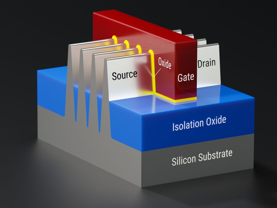
In a PMOS transistor, the source and drain regions are doped with p-type semiconductor material, while the substrate is doped with n-type material. Conversely, in an NMOS transistor, the source and drain regions are doped with n-type semiconductor material, and the substrate is doped with p-type material. The gate is electrically isolated from the substrate by a thin insulating layer, typically silicon dioxide (SiO2).
PMOS and NMOS transistors function as voltage-controlled switches or amplifiers, allowing or blocking current flow between the source and drain based on the gate voltage. The key difference lies in the type of charge carriers responsible for the current flow: holes (positive charges) in PMOS and electrons (negative charges) in NMOS. Additionally, the polarity of the voltages applied to the terminals differ between the two types. PMOS transistors are typically "on" when the gate voltage is low (or negative) relative to the source, while NMOS transistors are "on" when the gate voltage is high (or positive) relative to the source.
The Semiconductor Backbone
The foundation of PMOS and NMOS transistors lies in the semiconductor materials used for fabrication. Silicon (Si) is the most commonly used semiconductor, due to its abundance, suitable electrical properties, and well-established manufacturing processes. Silicon has a diamond cubic crystal structure, allowing precise control of its electrical properties through doping.

Gallium arsenide (GaAs) is another semiconductor material used in transistor fabrication. GaAs has higher electron mobility compared to silicon, making it suitable for high-frequency and high-speed applications, but it is more expensive and less abundant.
Doping involves the intentional introduction of impurities (dopants) into the semiconductor lattice to alter its electrical properties. For silicon, boron is commonly used for p-type doping, while phosphorus or arsenic is used for n-type doping.
In p-type doping, dopant atoms like boron create holes, which are the majority charge carriers. The concentration of holes is directly proportional to the dopant concentration. Conversely, in n-type doping, dopant atoms like phosphorus or arsenic donate electrons, making electrons the majority charge carriers. The concentration of electrons is directly proportional to the dopant concentration.
The doping process is typically carried out using ion implantation or diffusion techniques. Ion implantation involves accelerating dopant ions towards the semiconductor surface, allowing precise control over dopant concentration and distribution. Diffusion involves exposing the semiconductor to a high-temperature environment containing dopant atoms, allowing them to diffuse into the material.
By carefully controlling the doping process and dopant concentrations, engineers can tailor the electrical properties of the semiconductor material to suit the specific requirements of PMOS and NMOS transistors.
Recommended Reading: Understanding Transistors: What They Are and How They Work
Structural Differences: A Closer Look
PMOS Transistor Structure
A PMOS transistor is constructed on a semiconductor substrate, typically made of n-type silicon. The source and drain regions are formed by introducing p-type dopants, such as boron, into the substrate. These p-type regions are separated by a channel region, which is part of the n-type substrate.
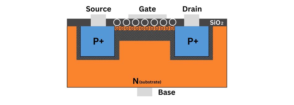
Above the channel region lies the gate, separated from the substrate by a thin layer of insulating material, typically silicon dioxide (SiO2). The gate is usually made of a highly conductive material, such as polycrystalline silicon or a metal.
When a voltage is applied between the source and drain terminals, a depletion region forms at the junction between the p-type source/drain regions and the n-type substrate. [2] This depletion region is an area where the majority charge carriers (holes in the p-type regions and electrons in the n-type substrate) have been swept away, leaving behind a region depleted of mobile charge carriers.
The depletion region acts as an insulating barrier, preventing current flow between the source and drain. However, when a sufficient voltage is applied to the gate terminal, an electric field is created in the channel region, attracting holes from the p-type source and drain regions. As the gate voltage increases, more holes accumulate in the channel region, forming a conductive path between the source and drain, allowing current to flow.
NMOS Transistor Structure
The structure of an NMOS transistor is similar to that of a PMOS transistor, but with the doping types and configurations reversed. In an NMOS transistor, the source and drain regions are formed by introducing n-type dopants, such as phosphorus or arsenic, into a p-type semiconductor substrate, typically made of silicon.
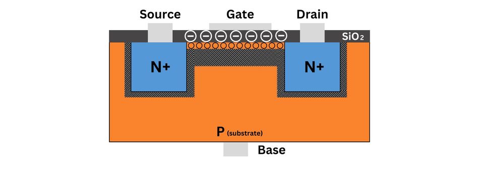
The n-type source and drain regions are separated by a channel region, which is part of the p-type substrate. Above the channel region lies the gate, which is separated from the substrate by a thin layer of insulating material, typically SiO2. The gate is typically made of a highly conductive material, such as polycrystalline silicon or a metal.
When a voltage is applied between the source and drain terminals, a depletion region forms at the junction between the n-type source/drain regions and the p-type substrate. This depletion region is a region where the majority charge carriers (electrons in the n-type regions and holes in the p-type substrate) have been swept away, leaving behind a region depleted of mobile charge carriers.
The depletion region acts as an insulating barrier, preventing the flow of current between the source and drain. However, when a sufficient voltage is applied to the gate terminal, an electric field is created in the channel region, attracting electrons from the n-type source and drain regions. As the gate voltage increases, more electrons accumulate in the channel region, forming a conductive path between the source and drain, allowing current to flow.
Operating Principles: How PMOS and NMOS Work
PMOS Operating Mechanism
The operating principle of a PMOS transistor revolves around the control of the conduction channel between the source and drain terminals by the voltage applied to the gate terminal. In a PMOS device, the charge carriers responsible for current flow are holes, which are positively charged.
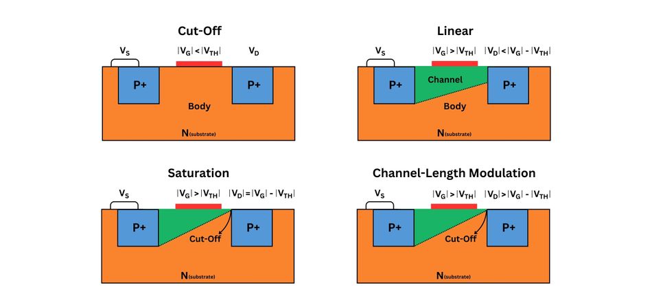
When no voltage is applied to the gate (VGS = 0V), the transistor is in its default "on" state, allowing current to flow when a voltage is applied between the source and drain terminals. The p-type source and drain regions have a high concentration of holes, which can freely move through the channel region.
To turn the PMOS transistor off, a negative voltage is applied to the gate terminal (VGS < 0V). [3] This negative voltage creates an electric field that repels the positively charged holes from the channel region, increasing the width of the depletion region. As the gate voltage becomes more negative, the depletion region widens, effectively pinching off the conduction channel and preventing current flow.
The threshold voltage (Vth) is a critical parameter in PMOS transistor operation. It is the minimum gate-to-source voltage required to create a conductive channel between the source and drain. For a PMOS transistor, the threshold voltage is negative, meaning that the transistor turns off when VGS is more negative than Vth.
By modulating the gate voltage, the width of the conduction channel can be controlled, allowing for the regulation of current flow between the source and drain. This voltage-controlled current flow forms the basis for the use of PMOS transistors in various electronic circuits, such as amplifiers, switches, and logic gates.
NMOS Operating Mechanism
The operating principle of an NMOS transistor is similar to that of a PMOS transistor, but with the charge carriers and voltage polarities reversed. In an NMOS device, the charge carriers responsible for current flow are electrons, which are negatively charged.
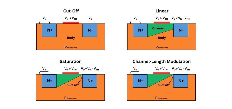
When no voltage is applied to the gate (VGS = 0V), the transistor is in its default "off" state, preventing current flow between the source and drain terminals. The n-type source and drain regions have a high concentration of electrons, but the channel region is depleted of mobile charge carriers.
To turn the NMOS transistor on, a positive voltage is applied to the gate terminal (VGS > 0V). This positive voltage creates an electric field that attracts the negatively charged electrons from the source and drain regions, forming a conductive channel in the channel region. As the gate voltage increases, more electrons accumulate in the channel region, increasing the width of the conduction channel and allowing more current to flow.
The threshold voltage (Vth) is a critical parameter. It is the minimum gate-to-source voltage required to create a conductive channel between the source and drain. For an NMOS transistor, the threshold voltage is positive, meaning that the transistor turns on when VGS is more positive than Vth.
By modulating the gate voltage, the width of the conduction channel can be controlled, allowing for the regulation of current flow between the source and drain. This voltage-controlled current flow forms the basis for the use of NMOS transistors in various electronic circuits.
Recommended Reading: Understanding NPN vs PNP Transistors: A Comprehensive Guide
NMOS and PMOS: Utilization
The NMOS and PMOS can be utilized as active loads, capacitors, voltage-controlled resistors, current reflectors, diodes, and even trans-impedance amplifiers. Let’s discuss the two most common applications: switches and voltage amplifiers.
Switch
NMOS and PMOS transistors, can both act like electronic switches. They control current flow between source and drain terminals by responding to the voltage on their gate.
Take the example of a light switch. NMOS is like a regular switch - applying a voltage (like flipping the switch) turns it on, allowing current (like light) to flow. Conversely, removing the voltage turns it off, stopping the current. PMOS works the other way around - a voltage turns it off, while no voltage lets the current flow.
These transistors are the backbone of digital logic circuits. By combining them, engineers can create basic building blocks like AND and OR gates, the foundation of digital devices. They're also useful for controlling signal flow and even heavy-duty power switching in applications like motor control.
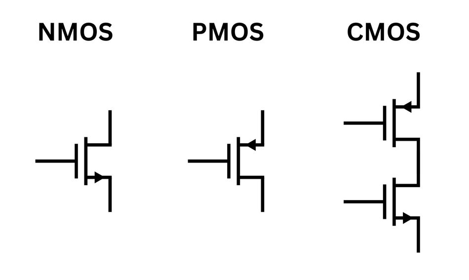
The real power comes from using both NMOS and PMOS together. This creates complementary metal oxide semiconductor (CMOS) logic, known for lower energy use and better resistance to electrical noise. It's like having two flavors of switches, offering more flexibility and optimization for different electronic needs. In short, these tiny transistors, with their switchable personalities, are essential for modern electronics.
Amplifier
Since NMOS and PMOS are both "voltage to current" converters, a voltage amplifier can be produced by merely connecting a resistive load to the current output. In contrast, for the drain current to serve as an appropriate current source, the drain current must be independent of the drain voltage (in other words, the output impedance should be high). The MOSFET must, therefore, operate in the saturation area to function as a voltage amplifier. The input signal should also be reduced to a minimum to prevent non-linear effects due to the existing equations' extreme non-linearity.
In an amplifier circuit, the input signal is applied to the gate terminal of the transistor. By adjusting the gate voltage, we can control the current flowing between the source and drain terminals of the transistor. This modulation of current based on the input signal is the key to amplification.
In conclusion, NMOS and PMOS transistors, by virtue of their ability to modulate current flow based on a voltage input, serve as essential building blocks for amplifier circuits. These circuits play a vital role in various applications that require amplifying weak signals, such as audio amplifiers, microprocessors, and communication systems.
Complementary MOS (CMOS) Technology
Complementary MOS (CMOS) technology is a widely used approach in modern electronics that combines both PMOS and NMOS transistors in a complementary configuration. In CMOS circuits, PMOS and NMOS transistors are arranged in a way that leverages their complementary behavior, where one type of transistor is on while the other is off, and vice versa.
One of the primary benefits of CMOS technology is its low power consumption. In a CMOS circuit, there is virtually no direct path between the supply voltage and ground when the circuit is in a steady state. This is because either the PMOS or NMOS transistor is in the off state, acting as an open circuit and preventing current flow. Power is only consumed during the switching transitions, when both transistors are temporarily on, allowing a brief current flow.
CMOS technology also offers high noise immunity, which is the ability to resist the effects of electrical noise and interference. [4] This is achieved through the complementary behavior of PMOS and NMOS transistors, where one type of transistor is more resistant to noise than the other. By combining both types of transistors, CMOS circuits can effectively cancel out the effects of noise, resulting in improved signal integrity and reliability.
Recommended Reading: Concurrent-Mode CMOS Detector IC for Sub-Terahertz Imaging System
Challenges and Considerations
Scaling and Miniaturization
One of the primary challenges associated with scaling down transistors is the short-channel effect. As the channel length between the source and drain regions decreases, the gate electrode loses some of its control over the channel, leading to increased leakage current and reduced transistor performance. This effect becomes more pronounced as the transistor dimensions approach the nanometer scale, making it difficult to maintain proper transistor operation.
Another challenge is gate leakage, which occurs when the gate oxide layer becomes too thin to effectively insulate the gate electrode from the channel. As transistors are scaled down, the gate oxide thickness must also be reduced to maintain proper gate control. However, when the gate oxide becomes too thin, electrons can tunnel through the insulating layer, resulting in increased leakage current and power dissipation.
Hot carrier effects also become more significant as transistors are miniaturized. As the electric field within the transistor increases due to shorter channel lengths, electrons can gain sufficient energy to overcome the barrier between the channel and the gate oxide. These high-energy electrons, known as hot carriers, can become trapped in the gate oxide or cause damage to the transistor structure, leading to performance degradation and reliability issues.
To mitigate these scaling challenges, several techniques have been developed. Strain engineering involves introducing mechanical stress into the transistor structure to improve carrier mobility and reduce leakage current. This can be achieved through the use of strained silicon layers or by incorporating materials with different lattice constants.
High-k dielectrics, such as hafnium oxide (HfO2), have been introduced to replace the traditional silicon dioxide (SiO2) gate oxide. These materials have a higher dielectric constant, allowing for a thicker gate oxide layer while maintaining the same capacitance, thus reducing gate leakage.
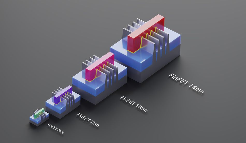
FinFET (Fin Field-Effect Transistor) structures have also been adopted to improve transistor performance and scalability. [5] In a FinFET, the channel is raised above the substrate, forming a thin, vertical fin that is surrounded by the gate electrode. This 3D structure provides better gate control, reduced leakage current, and improved performance compared to planar transistors.
Leakage Current and Power Dissipation
Leakage current is a significant challenge in PMOS and NMOS transistors, particularly as device dimensions continue to shrink. Leakage current refers to the unwanted flow of current through the transistor when it is supposed to be in the off state. This leakage contributes to increased power dissipation, which can have a detrimental impact on the overall power efficiency of the device.
One of the primary sources of leakage current is subthreshold leakage. Subthreshold leakage occurs when the gate voltage is below the threshold voltage (Vth) of the transistor. In this state, the transistor is not completely turned off, and a small amount of current can still flow between the source and drain. As transistor dimensions decrease, the threshold voltage also decreases, making it easier for subthreshold leakage to occur.
Another source of leakage current is gate-induced drain leakage (GIDL). GIDL occurs when there is a high electric field between the gate and the drain, causing electrons to tunnel from the drain to the substrate. This tunneling effect becomes more pronounced as the gate oxide thickness decreases, which is a common trend in transistor scaling.
To mitigate leakage current and improve power efficiency, several techniques and strategies have been developed. Power gating involves using additional transistors to disconnect the power supply from inactive circuits, significantly reducing leakage current and improving overall power efficiency.
Multi-threshold CMOS (MTCMOS) is another technique used to reduce leakage current. [6] In MTCMOS, transistors with different threshold voltages are used in the same circuit. High-threshold voltage transistors are used in the non-critical paths to reduce leakage current, while low-threshold voltage transistors are used in the critical paths to maintain performance.
Body biasing involves applying a voltage to the substrate (body) of the transistor to control its threshold voltage. By applying a reverse body bias, the threshold voltage can be increased, reducing subthreshold leakage. Conversely, applying a forward body bias can decrease the threshold voltage, improving performance at the cost of increased leakage.
Implementing these leakage reduction techniques requires careful design considerations and trade-offs. Power gating introduces additional transistors and control circuitry, which can increase the overall area and complexity of the circuit design. MTCMOS requires the use of multiple threshold voltages, which can complicate the fabrication process and increase manufacturing costs. Body biasing requires additional circuitry to generate and distribute the bias voltages, as well as careful characterization of the transistor behavior under different bias conditions.
Reliability and Aging Effects
As PMOS and NMOS transistors are subjected to prolonged use and stress, they can experience various reliability issues and aging effects that can degrade their performance and ultimately lead to device failure. Understanding these effects and developing methods to mitigate them is crucial for ensuring the long-term reliability and longevity of electronic devices.
One of the primary aging effects in transistors is hot carrier injection (HCI). HCI occurs when high-energy carriers (electrons or holes) gain sufficient kinetic energy to overcome the potential barrier and become injected into the gate oxide or the substrate. These injected carriers can create defects in the oxide, leading to a shift in the threshold voltage and a degradation of the transistor's performance over time. HCI is more prominent in NMOS transistors due to the higher mobility of electrons compared to holes.
Another significant reliability issue is bias temperature instability (BTI), which can manifest as negative BTI (NBTI) in PMOS transistors and positive BTI (PBTI) in NMOS transistors. BTI occurs when a transistor is subjected to a constant voltage stress at elevated temperatures. This stress can cause the formation of interface traps and oxide charges, leading to a shift in the threshold voltage and a reduction in the drain current. NBTI is more severe in PMOS transistors due to the presence of holes, while PBTI affects NMOS transistors.
Electromigration is another reliability concern in transistors, particularly in the metal interconnects. Electromigration is the transport of metal ions due to the flow of high-density electric current. Over time, this can lead to the formation of voids and hillocks in the metal lines, causing increased resistance, open circuits, or short circuits. Electromigration becomes more critical as the current density in the interconnects increases with transistor scaling.
To improve the reliability and longevity of PMOS and NMOS transistors, several methods have been developed. Stress engineering techniques, such as the use of silicon nitride capping layers or the incorporation of deuterium anneals, can help reduce the impact of HCI and BTI. Redundancy involves incorporating redundant transistors or circuits to mitigate the impact of individual transistor failures. Error correction techniques, such as error-correcting codes (ECC), can also be employed to improve reliability by detecting and correcting errors caused by transistor failures or other sources.
Recommended Reading: Semiconductor Fabrication Process: The Ultimate Guide to Creating Cutting-Edge Electronics
Conclusion
PMOS and NMOS transistors serve as the backbone of digital circuits, each with distinct differences in their structures, operating principles, and applications. PMOS transistors have p-type source and drain regions, while NMOS transistors have n-type source and drain regions. PMOS uses holes in p-type regions, while NMOS utilizes electrons in n-type regions. This leads to opposite gate voltage control: PMOS turns on with low gate voltage, NMOS with high voltage. Consequently, PMOS find use in analog circuits and power management, while NMOS excel in digital logic and high-frequency applications. Understanding these distinctions empowers engineers to design electronic circuits, ensuring optimal performance, power efficiency, and reliability.
Frequently Asked Questions
Q. What is the main difference between PMOS and NMOS transistors?
A. The main difference between PMOS and NMOS transistors lies in the doping types of their source and drain regions, as well as the type of charge carriers responsible for current flow. PMOS transistors have p-type source and drain regions, and the charge carriers are holes (positive charges), while NMOS transistors have n-type source and drain regions, and the charge carriers are electrons (negative charges).
Q. How does the gate voltage control the operation of PMOS and NMOS transistors?
A. In PMOS transistors, a negative gate voltage repels the positively charged holes from the channel region, effectively turning the transistor off. In NMOS transistors, a positive gate voltage attracts the negatively charged electrons, forming a conductive channel and turning the transistor on.
Q. What are some common applications of PMOS transistors?
A. PMOS transistors are commonly used in analog circuits, memory devices, and power management circuits, where their characteristics and performance are well-suited for these applications.
Q. What are some common applications of NMOS transistors?
A. NMOS transistors are widely used in digital logic circuits, power electronics, and high-frequency applications, where their characteristics and performance are well-suited for these applications.
Q. What is the significance of the threshold voltage in PMOS and NMOS transistors?
A. The threshold voltage is a critical parameter in both PMOS and NMOS transistors. It determines the minimum gate-to-source voltage required to create a conductive channel between the source and drain. For PMOS transistors, the threshold voltage is negative, while for NMOS transistors, it is positive. Understanding and controlling the threshold voltage is essential for proper transistor operation and performance optimization.
References
[1] allaboutcircuits. MOSFET Structure and Operation for Analog IC Design [Cited 2024 April 11] Available at: Link
[2] electronicsforu. What is a MOSFET? It’s Types, Working, Circuit, and Applications [Cited 2024 April 11] Available at: Link
[3] Wevolver. Understanding MOS Transistors: Fundamentals and Applications [Cited 2024 April 11] Available at: Link
[4] Medium. Importance of complementary metal oxide semiconductor (CMOS) [Cited 2024 April 11] Available at: Link
[5] NSR. New Structure Transistors for Advanced Technology Node CMOS ICs [Cited 2024 April 11] Available at: Link
[6] IEEE. High performance CMOS current comparator using MTCMOS technique design [Cited 2024 April 11] Available at: Link
in this article
1. Introduction2. The Fundamentals: PMOS and NMOS Transistors3. Structural Differences: A Closer Look4. Operating Principles: How PMOS and NMOS Work5. NMOS and PMOS: Utilization6. Complementary MOS (CMOS) Technology7. Challenges and Considerations8. Conclusion9. Frequently Asked Questions10. ReferencesNo time now? Save for later.
We only use your email to send this link. Privacy Policy.