NMOS and PMOS Transistors: Fundamentals and Applications
In this article, we will delve into the structure and operation of NMOS and PMOS transistors, and discuss the applications and characteristics of these essential components in electronic circuits.

09 May, 2023. 22 minutes read
Introduction
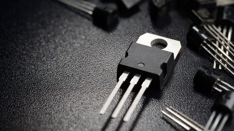
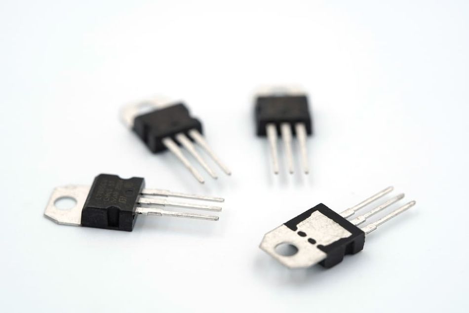
MOS (Metal-Oxide-Semiconductor)- NMOS (N-Channel MOS) and PMOS (P-Channel MOS) transistors play a crucial role in modern electronics. These transistors provide the basic building blocks for a wide range of devices, from microprocessors to memory chips. The most significant use of MOSFET transistors is in VLSI design due to their small size. A trillion MOSFETs are fabricated on a single chip. The development has led to significant advancements in technology and enabled the miniaturization of even more electronic components.
1. MOS Transistor Basics
An understanding of MOS transistor basics is crucial to grasp the operation and applications of these devices in modern electronics. In this section, we will explore the structure and operation of MOS transistors, discuss the differences between N-Channel MOS (NMOS) and P-Channel MOS (PMOS) transistors, and examine the key characteristics that define their performance in electronic circuits.
1.1 MOS Transistor Structure and Operation
Also known as MOSFET, there are two types of MOS transistors- depletion mode and Enhancement mode. The basic structure of a MOS transistor consists of three terminals: the gate, source, and drain. The gate terminal is separated from the semiconductor material by an insulating oxide layer, usually made of silicon dioxide (SiO2). This oxide layer plays a vital role in the operation of the transistor, as it prevents the flow of current directly between the gate and the semiconductor.
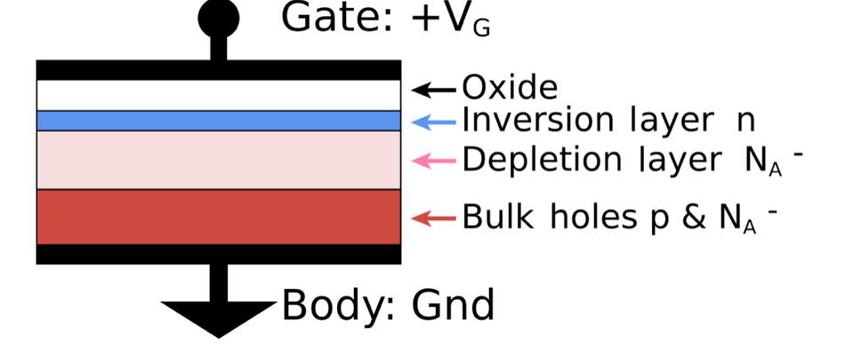
The semiconductor material is made up of typically silicon and is doped with impurities to create distinct regions with different electrical properties. These regions, known as the source and drain, are separated from each other and are in direct contact with the semiconductor region. When a voltage is applied to the gate terminal, an electric field is generated across the insulating oxide layer. The silicon dioxide layer enables the production of a capacitance “C” that later goes on to create a conducting channel inside the device. The polarity of the induced capacitor due to the dielectric SiO2 layer attracts negative charge carriers towards the gate terminal. Since electrons are the majority charge carriers in the N-regions, they move towards the metal under the gate terminal.
This electric field induces a change in the electrical properties of the channel region. The p-type channel under the gate terminal becomes more like an n-type region. The channel, also called an inversion layer, becomes conductive and enables the flow of current between the source and drain terminals. The conventional current flows from source to drain, opposite to the flow of electrons.
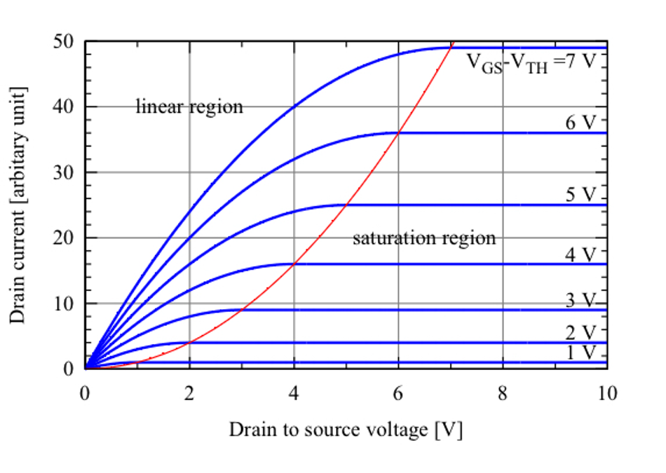
The ability to control the conductivity of the channel region with the gate voltage is the fundamental principle that allows MOS transistors to function as electronic switches. When a low voltage is applied below the threshold voltage, the channel remains non-conductive, and the transistor is in the "cut-off" state. Conversely, when the gate voltage exceeds this threshold, the channel becomes conductive, and the transistor is in the "on" state. Another case is when the input gate voltage becomes high enough, the channel increases the depletion layer width and behaves like a resistor. Very few electrons pass through the channel and current flow decreases in the device.
The operation of a MOS transistor is also influenced by the voltage difference between the source and drain terminals, known as the drain-source voltage (V_DS). As V_DS increases, the current flowing through the channel increases proportionally, up to a certain point known as the saturation region. In the saturation region, the current becomes constant and is primarily determined by the gate voltage, independent of the drain-source voltage.
This ability to modulate the flow of current between the source and drain terminals through the gate voltage enables MOS transistors to perform a wide range of functions in electronic circuits, such as amplification, switching, and digital logic operations.
1.2 N-Channel MOS (NMOS) and P-Channel MOS (PMOS)
In the realm of MOS transistors, there are two primary types: N-Channel MOS (NMOS) and P-Channel MOS (PMOS) transistors. Both types of transistors play a crucial role in the design of electronic circuits, with each having its unique characteristics and applications.
NMOS transistors are characterized by the use of an n-type (negatively doped) semiconductor material for the source and drain regions, while the substrate is made of p-type (positively doped) semiconductor material. When a positive voltage is applied to the gate terminal of an NMOS transistor, the electric field induced across the insulating oxide layer attracts free electrons in the p-type substrate, forming an n-type conductive channel between the source and drain regions. The conductivity of this channel increases with the gate voltage, allowing a higher current to flow between the source and drain terminals.
PMOS transistors, on the other hand, have a p-type semiconductor material for the source and drain regions, while the substrate is composed of n-type semiconductor material. When a negative voltage is applied to the gate terminal, the electric field across the insulating oxide layer attracts holes from the n-type substrate, creating a p-type conductive channel between the source and drain regions. The conductivity of this channel also increases with the magnitude of the gate voltage, but in the opposite direction compared to NMOS transistors.
One of the key differences between NMOS and PMOS transistors is their threshold voltage, which is the minimum voltage that must be applied to the gate terminal to induce a conductive channel. For NMOS transistors, the threshold voltage is typically positive, while for PMOS transistors, it is typically negative. This difference in threshold voltage can have significant implications for the design of electronic circuits, as it determines the voltage levels required to switch the transistors on and off.
The complementary nature of NMOS and PMOS devices is a defining feature of modern electronic circuit design. By combining both types of transistors in a single circuit, designers can create more efficient and versatile circuits with a wide range of functions. For example, complementary MOS (CMOS) technology, which we will discuss in detail later in this article, leverages the strengths of both NMOS and PMOS transistors to enable low-power and, high-performance digital circuits.
In addition to their complementary electrical characteristics, NMOS and PMOS transistors also exhibit differences in terms of their fabrication process and physical properties. For example, NMOS transistors generally have higher electron mobility than PMOS transistors, which results in faster switching speeds and better overall performance. However, this advantage comes at the cost of higher power consumption, making the choice between NMOS and PMOS transistors a critical consideration in the design of energy-efficient electronic systems.
1.3 MOS Transistor Characteristics
MOS transistors exhibit a range of characteristics that define their performance and suitability for various applications in electronic circuits. In this section, we will discuss some of the most important characteristics, such as the threshold voltage, transconductance, drain current, and output conductance. These parameters are listed in the transistor datasheet because understanding them is essential for designing effective circuits and applications.
Threshold Voltage
The threshold voltage (V_T)) is a critical characteristic of MOS transistors to determine the minimum gate voltage required to create a conductive channel between the source and drain terminals. The threshold voltage is influenced by several factors, including the doping concentration of the semiconductor material, the thickness of the oxide layer, and the work function difference between the gate and the substrate. In general, a lower threshold voltage allows the transistor to switch on and off more quickly, which can be beneficial for high-speed applications. However, this advantage comes at the expense of increased leakage current, which can lead to higher power consumption.
Transconductance
Transconductance (g_m) is another important characteristic of MOS transistors, as it quantifies the sensitivity of the drain current (I_D) to changes in the gate-source voltage (V_GS). In other words, transconductance measures how effectively the gate voltage controls the current flow between the source and drain terminals. A higher transconductance value implies that a small change in gate voltage will result in a larger change in drain current, leading to more efficient and precise control of the transistor's operation. Transconductance is influenced by factors such as the channel length, channel width, and temperature, as well as the specific type of transistor (NMOS or PMOS).
Drain Current
Drain current (I_D) is a key parameter that quantifies the amount of current flowing between the source and drain terminals of a MOS transistor. The drain current is primarily determined by the gate-source voltage, drain-source voltage, and the transistor's intrinsic characteristics like the threshold voltage and transconductance. The relationship between these variables can be described using mathematical models, such as the square-law model or the gradual channel approximation. These models can be used to predict the behaviour of MOS transistors in different operating conditions and guide the design of electronic circuits.
Output Characteristics: Output conductance (g_DS) is a measure of the dependency of the drain current on the drain-source voltage. It indicates the extent to which the current flowing through the transistor is affected by variations in the voltage across the source and drain terminals. In an ideal MOS transistor, the output conductance would be zero, meaning that the drain current would remain constant regardless of changes in the drain-source voltage. However, real transistors exhibit a non-zero output conductance due to various factors including channel length modulation and the presence of parasitic capacitances. Minimizing output conductance is important for achieving high linearity and output impedance in amplifier circuits.
In summary, understanding the key characteristics of MOS transistors like threshold voltage, transconductance, drain current, and output conductance, is essential for designing efficient and effective electronic circuits. By considering these parameters in the context of specific applications and performance requirements, engineers can optimize the performance of MOS transistors and create electronic systems that meet the demanding needs of modern technology.
Suggested Readings: Microcontroller Programming: Mastering the Foundation of Embedded Systems
2. PMOS Transistor Basics
PMOS transistors or PMOSFETs are a fundamental building block in electronic circuits and an essential counterpart to NMOS transistors. Like NMOS transistors, they function as voltage-controlled switches. These transistors allow or block the flow of current between the source and drain terminals in response to a voltage applied to the gate terminal. In this section, we will explore the basic structure and operation of PMOS transistors, and discuss how they differ from their NMOS counterparts.
2.1 PMOS Transistor Structure and Operation
The basic structure of a PMOS transistor consists of three terminals: the gate, source, and drain, as well as a substrate (or body region) made of n-type semiconductor material. The source and drain terminals are formed from p-type semiconductor material, which is created by introducing acceptor impurities, such as boron, into the n-type substrate. An insulating silicon dioxide layer is deposited on the substrate to separate it from the gate terminal, which is usually made of a conductive material like polysilicon or metal.
When a negative voltage is applied to the gate terminal relative to the source, an electric field is established across the oxide layer, attracting holes (positively charged carriers) from the n-type substrate toward the gate. As the gate voltage becomes more negative, the concentration of holes increases, eventually forming a conductive p-type channel between the source and drain regions. This channel allows current to flow between the source and drain terminals, effectively turning on the PMOS transistor.
One key distinction between PMOS and NMOS transistors lies in their threshold voltages. For a PMOS transistor, the threshold voltage is typically negative, whereas it is positive for an NMOS transistor. Consequently, a PMOS transistor is turned on by applying a negative gate-source voltage, while an NMOS transistor is turned on by applying a positive gate-source voltage. This complementary behaviour allows PMOS and NMOS transistors to be combined in various circuit configurations, enabling a wide range of electronic functions and improved energy efficiency.
Another important difference between PMOS and NMOS transistors is their carrier mobility. In PMOS transistors, the majority carriers are holes, which have lower mobility than the electrons that serve as the majority carriers in NMOS transistors. As a result, PMOS transistors generally exhibit slower switching speeds and lower performance compared to NMOS transistors. However, this trade-off can be offset by the advantages of using both types of transistors in complementary configurations, as seen in CMOS technology, which we will discuss later in this article.
In summary, PMOS transistors are a crucial component in modern electronic circuits, providing complementary functionality to NMOS transistors. Their basic structure and operation are similar to NMOS devices but with important differences in threshold voltage, carrier mobility, and the type of majority carriers. Understanding these distinctions is essential for designing efficient and versatile electronic systems that leverage the strengths of both PMOS and NMOS transistors.
 Types of MOSFET 2.2 PMOS Transistor Characteristics
The electrical characteristics of a PMOS transistor determine its performance in a circuit and can be described by several key parameters. These parameters are essential to understanding the behaviour of PMOS transistors and how they interact with other components in electronic circuits. All these parameters and characteristics are listed in the PMOS datasheet. In this section, we will discuss some of the most important characteristics of PMOS transistors like the threshold voltage, drain current, and transconductance.
Threshold Voltage (Vth)
The threshold voltage, denoted as Vth, is a critical parameter that defines the gate-source voltage at which a PMOS transistor starts to conduct current between its source and drain terminals. For PMOS transistors, the threshold voltage is typically negative, and the transistor is turned on when the gate-source voltage is more negative than the threshold voltage. The threshold voltage can be affected by factors such as temperature, manufacturing process variations, and the dopant concentration in the semiconductor material.
Drain Current (ID)
The drain current, ID, is the current flowing through the PMOS transistor when it is in the conducting state. The magnitude of the drain current depends on the gate-source voltage (Vgs), drain-source voltage (Vds), and various device parameters. One useful model for describing the drain current in PMOS transistors is the following current equation:
ID = μp * Cox * (W/L) * [(Vgs - Vth) * Vds - (1/2) * Vds^2]
In this equation, μp represents the hole mobility, Cox is the oxide capacitance per unit area, W is the channel width, and L is the channel length. The drain current is proportional to the difference between the gate-source voltage and the threshold voltage (Vgs - Vth) and the drain-source voltage (Vds).
Transconductance (gm)
Transconductance, denoted as gm, is a measure of a PMOS transistor's ability to convert changes in gate-source voltage into changes in drain current. It is an essential parameter for analyzing the performance of amplifiers and other analog circuits. Transconductance can be defined as the ratio of the change in drain current (ΔID) to the change in gate-source voltage (ΔVgs):
gm = ΔID / ΔVgs
In the linear region of operation, the transconductance of a PMOS transistor can be calculated using the following equation:
gm = μp * Cox * (W/L) * (Vgs - Vth)
Subthreshold Swing (SS)
Subthreshold swing is a parameter that quantifies the sharpness of the transition between the off and on states of a PMOS transistor. It is typically expressed in mV/decade and is defined as the change in gate-source voltage required to change the drain current by one order of magnitude in the subthreshold region. Smaller values of subthreshold swing indicate a sharper transition, which is generally desirable for low-power applications and faster switching.
By understanding these key characteristics of PMOS transistors, designers can predict their performance in a variety of circuits and make informed decisions when selecting and optimizing devices for specific applications. The interplay of these parameters, along with external factors such as temperature, supply voltage, and process variations, ultimately determines the efficiency, speed, and reliability of electronic systems built with PMOS transistors.
CMOS (Complementary Metal-Oxide-Semiconductor) technology is a widely used semiconductor technology that leverages both NMOS and PMOS transistors in integrated circuits. The complementary nature of these two types of transistors enables designers to create highly efficient and low-power electronic devices. This section will cover the fundamental concepts of CMOS technology, including the benefits it offers compared to other semiconductor technologies, and the principles of CMOS circuit design.
3. CMOS Technology
3.1 Complementary MOS (CMOS) Circuit Design
Complementary MOS circuit design is the process of creating electronic circuits using both NMOS and PMOS transistors in a complementary manner. This approach takes advantage of the unique properties of both transistor types to achieve high performance, low power consumption, and noise immunity. The primary concept in CMOS circuit design is the use of complementary transistor pairs, where one transistor type is used to pull the output voltage up, while the other is used to pull it down.
Pull-up and Pull-down Networks
In a CMOS circuit, the pull-up network consists of one or more PMOS transistors connected between the output node and the positive supply voltage (Vdd). When the input voltage is low, the PMOS transistors turn on and provide a path for current to flow from Vdd to the output node, pulling the output voltage high. Conversely, the pull-down network consists of one or more NMOS transistors connected between the output node and ground (GND). When the input voltage is high, the NMOS transistors turn on and provide a path for current to flow from the output node to GND, pulling the output voltage low.
CMOS Inverter
A fundamental building block of CMOS circuit design is the CMOS inverter, which is a simple logic gate that inverts the input signal. The CMOS inverter consists of a single PMOS transistor in the pull-up network and a single NMOS transistor in the pull-down network. When the input voltage is low, the PMOS transistor turns on and the NMOS transistor turns off, resulting in a high output voltage. Conversely, when the input voltage is high, the PMOS transistor turns off and the NMOS transistor turns on, resulting in a low output voltage.
Complex CMOS Gates
More complex CMOS gates, such as NAND, NOR, XOR, and XNOR, can be constructed by combining multiple pull-up and pull-down networks with various input configurations. For instance, a two-input CMOS NAND gate consists of two parallel PMOS transistors in the pull-up network and two series-connected NMOS transistors in the pull-down network. The output voltage of the NAND gate is high only when both input voltages are low, which is the inverted behaviour of the AND function.
Advantages of CMOS Technology
CMOS technology offers several advantages over other semiconductor technologies like diodes and bipolar junction transistors (BJT). It makes CMOS the preferred choice for modern integrated circuits. Some of the main benefits of CMOS technology include:
Low static power consumption: Due to the complementary nature of the pull-up and pull-down networks, there is virtually no static power consumption in CMOS circuits when they are not switching. This leads to significant power savings, especially in battery-operated devices.
High noise immunity: CMOS circuits have a wide noise margin, making them less susceptible to interference from external sources or noise within the circuit itself.
Scalability: CMOS technology has proven to be highly scalable, enabling the development of increasingly smaller and more complex integrated circuits with each new generation of semiconductor fabrication processes.
By understanding the principles of CMOS circuit design and leveraging the unique properties of NMOS and PMOS transistors, designers can create highly efficient and low-power electronic devices using CMOS technology. The complementary transistor pairs ensure that only one of the transistors in the pair is on at any given time, minimizing power consumption during the switching process. Furthermore, CMOS technology enables the creation of complex logic gates and circuits, offering flexibility and adaptability to various applications.
3.2 CMOS Logic Gates
CMOS logic gates are fundamental building blocks for digital circuits and systems, providing the ability to perform various logical operations on input signals. By leveraging the properties of CMOS technology, these gates can achieve high performance, low power consumption, and excellent noise immunity. In this section, we will discuss the design and operation of common CMOS logic gates, including the inverter NOT, NAND, NOR, XOR, and XNOR gates.
CMOS Inverter
The CMOS inverter is the simplest and most fundamental logic gate. It consists of a single PMOS transistor in the pull-up network and a single NMOS transistor in the pull-down network. When the input voltage is low, the PMOS transistor turns on, and the NMOS transistor turns off, resulting in a high output voltage. Conversely, when the input voltage is high, the PMOS transistor turns off, and the NMOS transistor turns on, resulting in a low output voltage.
CMOS NAND Gate
A CMOS NAND gate is a logic gate that performs the inverted AND function. A two-input CMOS NAND gate consists of two parallel PMOS transistors in the pull-up network and two series-connected NMOS transistors in the pull-down network. The output voltage of the NAND gate is high only when both input voltages are low. When either or both input voltages are high, the output voltage is low.
The NAND gate can be easily extended to accommodate more inputs by adding additional parallel PMOS transistors and series-connected NMOS transistors. The output voltage of an n-input NAND gate is high only when all n-input voltages are low.
CMOS NOR Gate
A CMOS NOR gate is a logic gate that performs the inverted OR function. A two-input CMOS NOR gate consists of two series-connected PMOS transistors in the pull-up network and two parallel NMOS transistors in the pull-down network. The output voltage of the NOR gate is high only when both input voltages are low. When either or both input voltages are high, the output voltage is low.
Like the NAND gate, the NOR gate can be extended to accommodate more inputs by adding additional series-connected PMOS transistors and parallel NMOS transistors. The output voltage of an n-input NOR gate is high only when all n-input voltages are low.
CMOS XOR Gate
The CMOS XOR (exclusive-OR) gate is a more complex logic gate that performs the XOR function. It outputs a high voltage only when the input voltages are different. A two-input CMOS XOR gate can be constructed using a combination of NAND, NOR, and AND gates, resulting in a more complex transistor arrangement. The XOR gate's output voltage is low when both input voltages are the same (high or low), and high when the input voltages are different.
CMOS XNOR Gate
The CMOS XNOR (exclusive-NOR) gate is a logic gate that performs the inverted XOR function. It outputs a high voltage only when the input voltages are the same. A two-input CMOS XNOR gate can be constructed using a combination of NAND, NOR, and OR gates, resulting in a complex transistor arrangement similar to the XOR gate. The XNOR gate's output voltage is high when both input voltages are the same (high or low), and low when the input voltages are different.
Integrated circuits (ICs) are the backbone of modern electronics, consisting of millions or even billions of transistors interconnected to perform complex functions. MOS and PMOS transistors are the fundamental components of these ICs, used to build digital and analog circuits that power devices like smartphones, computers, and IoT devices. The process of creating ICs involves several steps, including the fabrication of MOS and PMOS transistors on a semiconductor substrate, the interconnection of these transistors, and the packaging of the resulting completed IC.
4. NMOS and PMOS Transistors in Integrated circuits
4.1 Fabrication Process
The fabrication process of MOS and PMOS transistors involves several steps, which can be broadly categorized into the following phases: material preparation, transistor formation, and interconnection.
Material Preparation: The process begins with the preparation of a semiconductor substrate, typically silicon. A thin layer of silicon dioxide (SiO2) is grown on the surface of the substrate through a process called oxidation. This oxide layer serves as an insulator and helps define the active regions where transistors will be formed. A layer of silicon nitride (Si3N4) may also be deposited on top of the oxide to further protect and stabilize the surface.
Transistor Formation
The formation of MOS and PMOS transistors involves several steps, including the creation of the gate, source, and drain regions. A layer of polysilicon is deposited on the oxide layer and then patterned using a process called photolithography. This pattern defines the gate regions of the transistors. Next, ion implantation is used to selectively dope the silicon substrate with impurities, creating the source and drain regions of the transistors. The doping process depends on whether the transistor is an NMOS or a PMOS device. For NMOS transistors, phosphorus or arsenic ions are implanted to create n-type regions, while for PMOS transistors, boron ions are implanted to create p-type regions.
Following the formation of the gate, source, and drain regions, a thin insulating layer called the gate oxide is grown between the gate and the silicon substrate. This layer is crucial for the proper functioning of the transistor, as it prevents current leakage between the gate and the channel when the transistor is off.
Interconnection
Once the MOS and PMOS transistors have been formed, the next step is to interconnect them to form functional circuits. A thin layer of metal, typically aluminium or copper, is deposited on the surface of the substrate and patterned using photolithography to create interconnections between transistors. Multiple layers of interconnects can be created by depositing additional layers of insulating and conductive materials and patterning them accordingly.
After the interconnects are formed, the completed IC undergoes various tests and inspections to ensure proper functionality and quality. Finally, the IC is packaged into a protective housing and prepared for use in electronic devices. The packaging process involves attaching the IC to a package substrate, connecting the package's pins to the IC's interconnects, and sealing the IC within a protective casing. This completed package can then be mounted on a printed circuit board (PCB) and integrated into an electronic system.
4.2 Scaling and Moore's Law
Scaling has been a driving force in the semiconductor industry, enabling the continuous improvement of IC performance, power efficiency, and cost-effectiveness. The concept of scaling refers to the miniaturization of transistor dimensions, which allows for the integration of a higher number of transistors on a single chip, leading to increased computational power and functionality. This phenomenon is closely related to Moore's Law, a prediction made by Gordon Moore, one of the co-founders of Intel. Moore's Law (1965) states that the number of transistors on an IC would double approximately every two years, resulting in exponential growth in IC performance and a reduction in cost per transistor.
The scaling process involves reducing the dimensions of the transistor, such as the gate length, channel width, and oxide thickness while maintaining or improving its electrical properties. As transistors become smaller, their performance improves due to factors such as reduced capacitance and resistance, leading to faster switching times and lower power consumption. However, scaling also presents several challenges, including increased leakage currents, short-channel effects, insulating problems, quantum tunnelling, and process variability, which can impact transistor performance and reliability.
To overcome these challenges, the semiconductor industry has employed various techniques and innovations, such as the introduction of new materials, device architectures, and manufacturing processes. For example, high-K dielectric materials have been introduced to replace traditional silicon dioxide gate dielectrics, providing a higher dielectric constant and reducing gate leakage currents. Additionally, new transistor architectures like FinFETs (Fin Field-Effect Transistors) have been developed to mitigate short-channel effects and improve electrostatic control in sub-10 nm technology nodes. Another architecture CasFET is expected to reduce minimisation challenges.
Although Moore's Law has driven the semiconductor industry for decades, it is widely acknowledged that it cannot continue indefinitely due to fundamental physical limits and economic factors. As the dimensions of transistors approach atomic scales, issues such as quantum tunnelling and manufacturing variability become increasingly challenging to overcome. Moreover, the cost of developing and building new fabrication facilities has risen significantly, making it more difficult for companies to maintain the pace of innovation and scaling dictated by Moore's Law.
Despite these challenges, researchers and engineers continue to explore alternative technologies and paradigms to maintain the growth of computational power, such as three-dimensional (3D) integration, neuromorphic computing, and quantum computing. These emerging technologies may provide new avenues to overcome the limitations of traditional scaling and extend the benefits of Moore's Law into the future.
Suggested Reading: FGPA Design- A comprehensive guide to mastering field programmable gate arrays
4.3 Applications of MOS and PMOS Transistors
MOS and PMOS transistors are the fundamental building blocks of modern electronic systems, serving a wide range of applications across various industries. By leveraging their unique characteristics, designers create circuits and systems to address specific needs and requirements.
Digital circuits are a primary application for MOS and PMOS transistors. Both NMOS and PMOS devices are used to construct logic gates, such as AND, OR, and XOR. They can be used for more complex circuits like flip-flops, registers, and multiplexers. The combination of these basic elements forms the foundation of digital systems, including microprocessors, memory chips, and application-specific integrated circuits (ASICs).
In the realm of analog circuits, MOS and PMOS transistors find use as amplifiers, filters, and oscillators. For instance, operational amplifiers (op-amps) often employ complementary MOS technology for their input and output stages, providing high gain, low noise, and excellent linearity. Additionally, voltage-controlled oscillators (VCOs) and phase-locked loops (PLLs), which are essential components in frequency synthesis and clock generation, rely on MOS transistors for precise tuning and control.
Power electronics is another important application area for MOS and PMOS transistors. Power MOSFETs (Metal-Oxide-Semiconductor Field-Effect Transistors) and IGBTs (Insulated-Gate Bipolar Transistors) are commonly used in power converters, motor drives, and switching regulators due to their high switching speeds, low on-resistance, and efficient energy management. The ability to handle high current and voltage levels makes these devices suitable for applications ranging from consumer electronics to electric vehicles and renewable energy systems.
MOS and PMOS transistors also play a crucial role in sensing and actuation systems, such as those found in robotics, aerospace, and industrial automation. Transistors can be integrated with sensors, like photodetectors, accelerometers, and temperature sensors, to provide signal conditioning and processing, ensuring accurate and reliable measurements. In actuation systems, transistors are employed in driving actuators, like motors, solenoids, and piezoelectric elements, enabling precise control of mechanical systems.
In the field of radio frequency (RF) and microwave engineering, MOS and PMOS transistors are utilized to design oscillators, mixers, and amplifiers for wireless communication and radar systems. The development of RF CMOS technology has enabled the integration of RF and baseband circuits on a single chip, leading to compact, low-cost, and power-efficient transceivers for modern communication systems, such as 5G networks and Internet of Things (IoT) devices.
In summary, MOS and PMOS transistors serve as versatile and indispensable components in a wide variety of electronic systems, spanning from digital and analog circuits to power electronics and RF applications. As the semiconductor industry continues to evolve and innovate, these transistors will remain at the forefront of technological advancements, enabling new solutions and applications across multiple domains.
Conclusion
MOS and PMOS transistors have had a transformative impact on the electronics industry. These devices are at the core of various applications, ranging from digital and analog circuits to power electronics, sensing, actuation, and RF systems. The ongoing evolution of transistor technology is driven by innovations in materials and fabrication processes. It has enabled the creation of more compact, efficient, and high-performance electronic systems. As the industry continues to push the boundaries of what is possible, MOS and PMOS transistors will remain essential components, facilitating new advancements in a wide array of applications.
Frequently Asked Questions (FAQs)
What is the difference between NMOS and PMOS transistors?
NMOS (N-Channel Metal-Oxide-Semiconductor) and PMOS (P-Channel Metal-Oxide-Semiconductor) transistors are two types of MOSFETs that differ in the type of semiconductor material used for the channel. NMOS transistors utilize n-type material, while PMOS transistors use p-type material of the substrate. An n-type conducting channel is created in NMOS while the p-type conducting channel is created in a PMOS. Consequently, NMOS transistors are turned on by applying a positive voltage to the gate, while PMOS transistors are turned on by applying a negative voltage to the gate.
What is CMOS technology?
A: CMOS (Complementary Metal-Oxide-Semiconductor) technology is a fabrication process that combines both NMOS and PMOS transistors on the same integrated circuit. By employing complementary pairs of transistors in the design, CMOS circuits can achieve low power consumption, high noise immunity, and excellent scalability. It makes them suitable for a wide range of applications, including digital and analog systems.
What are MOS and PMOS transistors used for?
MOS and PMOS transistors are employed in various applications, including:
- Digital circuits: Logic gates, microprocessors, memory chips
- Analog circuits: Amplifiers, filters, oscillators
- Power electronics: Power converters, motor drives
- Sensing and actuation systems: Robotics, aerospace, industrial automation.
- RF systems: Wireless communication, radar.
How has Moore's Law impacted the development of MOS and PMOS transistors?
Moore's Law predicts the doubling of transistor density on an integrated circuit approximately every two years. It has driven the miniaturization and performance improvements of MOS and PMOS transistors. Scaling down transistor dimensions has led to reduced power consumption, increased switching speed, and higher integration levels, allowing for the creation of more complex and powerful electronic systems.
What are the main fabrication steps in the creation of MOS and PMOS transistors?
The fabrication of MOS and PMOS transistors involves a series of processes, including substrate preparation, oxidation, photolithography, etching, doping, and metallization. These steps enable the creation of the transistor's gate, source, drain, and channel regions, as well as the formation of electrical contacts and interconnections between devices on the integrated circuit.
References
Robert L. Boylestad & Louis Nashelsky (2021). Electronic Devices and Circuit Theory (Standard Edition). Pearson
Sedra, A. S. & Smith, K. C. (2004). Microelectronic circuits (5th ed.). New York: Oxford University Press
Nadine Collaert (2018). High Mobility Materials for CMOS Applications (1st edition). Woodhead Publishing Series in Electronic and Optical Materials.
https://www.sciencedirect.com/topics/engineering/complementary-metal-oxide-semiconductor