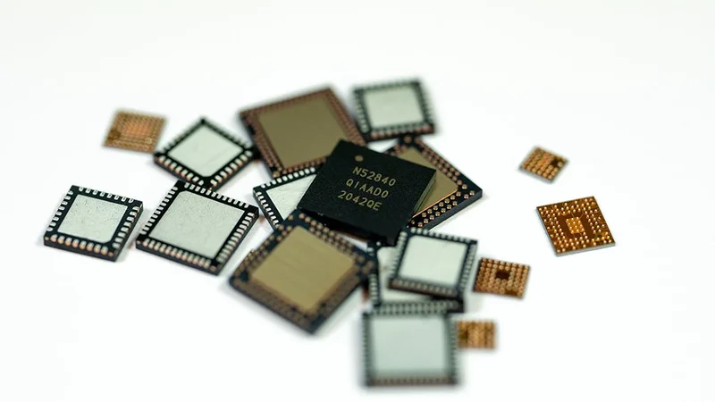
QFN and aQFN options for the nRF52840
For most of our nRF52 Series, we have a chip-scale package and a Quad-Flat No-leads (QFN) option. With our nRF52840, we introduced the aQFN package to our product portfolio.
03 Nov, 2021. 6 minutes read
This article was first published on
blog.nordicsemi.comFor most of our nRF52 Series, we have a chip-scale package and a Quad-Flat No-leads (QFN) option. With our nRF52840, we introduced the aQFN package to our product portfolio. We also decided to offer the same device in a QFN package, so Nordic customers now have the option of using nRF52840 in QFN48. This has just been released to the market.
There are two ways of looking at this new option. You can see it as a less complex nRF52840 with fewer pins and 1.7-3.6V supply voltage for our customers that don’t need USB and don’t need to run directly off Li-Ion batteries. It is also similar to an nRF52832 with additional security features, more flash and RAM as well as Zigbee and Thread support.
I used this opportunity to read up on different package options, and reeducate myself. I will share with you what I learned.
Then and now
The first microcontroller I got in contact with was in a Dual in-line package (DIP). You don’t see them much nowadays, but DIP packages are still beloved by hobbyists. They are easy to solder, and you can do a software update with a screwdriver. Just pop out the microcontroller with a screwdriver and put a new one with updated software into the socket. This is not a modern or resource-friendly approach, but it works if you sell <1000 devices a year that do not need much intelligence. One company I know of still uses this method in some of their older machines.
On today’s microcontrollers, you mostly see Quad Flat Packages (QFP), QFN, and Wafer Level Chip Scale Packages (WLCSP). When it comes to QFP, you will see a lot of Low profile Quad Flat Packages (LQFP) and Thin Quad Flat Packages (TQFP). These are surface-mounted packages with the leads extended out to the four sides of the package.
They have been around for decades and are still widely used. They are still solderable by hand (which I do not recommend), and the extended leads allow for visual inspection after assembly. They also make the solder joints more resilient to thermal and mechanical stress than leadless packages.
The extended leads are also what cause trouble with these packages. If one of the leads gets bent during transport or assembly, that integrated circuit (IC) becomes unusable for automated assembly. Having all the pins on the side of the package also leads to bigger packages in general.
The length of the pins is also why you do not see Nordic using any QFP package variants. The length impacts the inductance. Moreover, the capacitance between the pins is heavily impacted as the pins are parallel to each other. This increases the noise levels and coupling between the pins, particularly for devices using GHz radio.
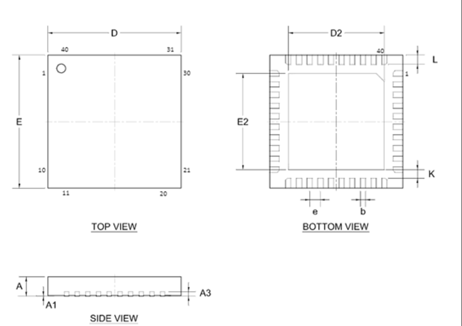
QFN
QFN packages, as the name suggests, do not have extended leads. This reduces the coupling and noise between the pins. The contacts to the PCB are on the bottom of the package. Most packages also have an exposed thermal pad on the bottom, attached to the IC. It is usually grounded, which reduces the noise level further.
QFN packages are a lot smaller than QFP-variants with the same number of pins. Some benefits are clear, like the smaller footprint and lower weight. No external leads and shorter bond wires mean reduced lead inductance. Besides, less metal is used since most bond wires use gold or copper.
In short: Smaller package and better thermal and electrical performance, but visual inspection gets harder.
WLSCP
Array-type packages is the way to go for devices requiring high pin density. BGA is mostly used for big processors with hundreds of pins. For that reason, I will not write too much about BGA itself but focus on WLCSP here.
When you read Chip-scale, it usually means the package is not more than 20% larger than the die itself. I mentioned before that QFN was a small package compared to other options. Let me put that into perspective. For our nRF52832, the QFN48 is 6x6 mm, and the WLCSP is 3.0x3.2 mm. So, the WLCSP is less than 30% of the area of the QFN. The pins are on the bottom of the chip and not only on the sides, which means we can drastically reduce the size and don’t have to use bond wires.
For WLSCP, the die will be painted with UV protective paint, or a thin plastic layer is added on the top of the chip. To make the pins accessible, we add wiring to the bottom and place the lead balls like in a BGA.
WLCSP is mostly chosen because of cost or size. It’s generally the cheapest option for the manufacturer, although varying with die size, pin count, etc. A 73-pin device will be more expensive than the same die with only 48 pins.
WLCSP denseness usually requires more aggressive PCB designs. For a smaller design, you will also need via in pad or buried vias. This is great for reducing size but drives assembly costs up. However, since these are usually needed for size-constrained devices, this is not an added cost of the WLCSP.
The main drawbacks are less resilience to mechanical stress and a more complex assembly process with additional layers on the PCB.
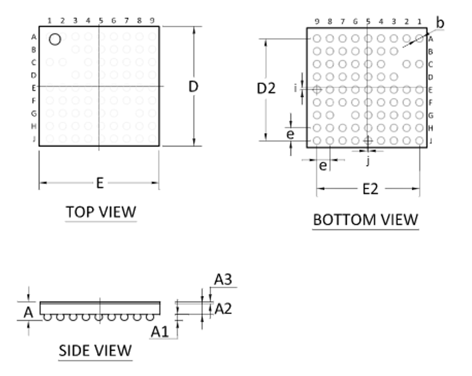
QFN or aQFN
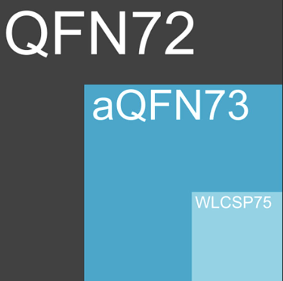
Advanced Quad Flat No-lead (aQFN) is an improvement on the QFN for higher pin counts. It has multiple rows of pins on the bottom of the package as well as the exposed thermal pad. A 73 pin package would then be 9x9 mm or 10x10 mm as a QFN72 and about half as an aQFN73 (7x7 mm).
With this package, we have even shorter bond wires than with the QFN and, therefore, less inductance. Again, a step up in terms of thermal and electrical performance.
The main drawback with an aQFN package compared with a QFN package is that it requires more advanced PCBs. We typically see the need to go to 4 layers as well as more aggressive via and track width rules to be able to use all the pins, especially the pins on the inner ring.

To give you an idea of the different sizes, here is a comparison of a QFN, an aQFN, and a WLCSP with similar pin count.
What does the PCB look like?
To finish off the package overview, let’s look at some PCB designs for different packages. I have selected one of our nRF52833 reference layouts for each package option. We have a QFN, an aQFN, and a WLCSP package for the nRF52833.
If you want to look at them for yourself, we have reference layouts for all our products in the downloads part of the product page. This is where you’ll find the layouts I show here.
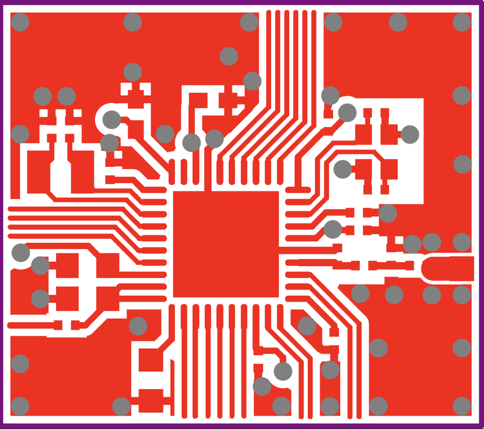
This picture shows that we can break out the device and route all signals on one layer when using a QFN. You then use vias to ground the thermal pad. Those vias help reduce the inductance and improve thermal coupling as well as improve the mechanical attachment of the SoC.
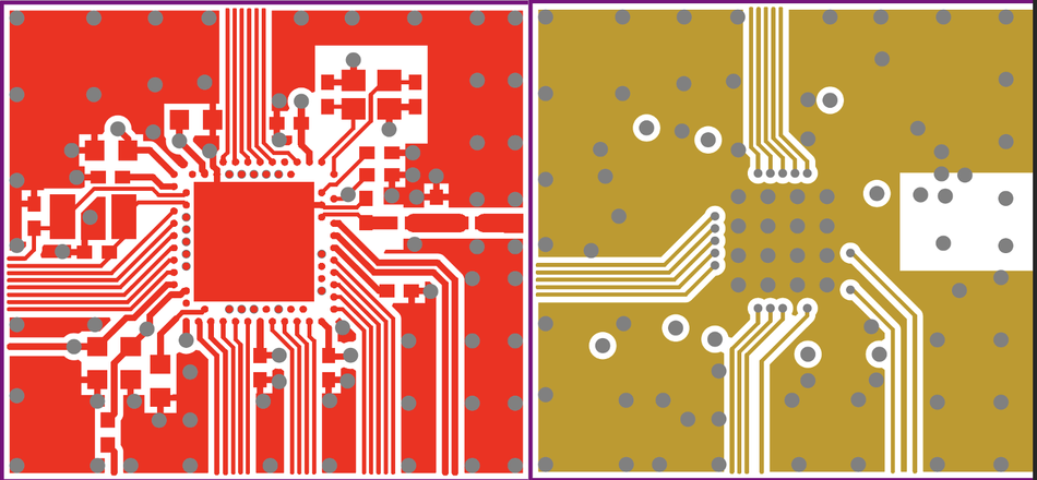
If you are using an aQFN, you have the pins in two rows underneath the SoC. You will need at least two separated layers to route all signals. However, the area we use on the PCB is smaller, and we can place additional components closer to the Soc because we do the routing underneath.
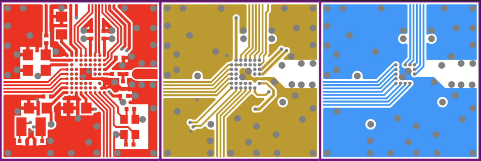
If we now look at one of the reference designs for the WLCSP, we can see that we need another additional layer to access all the device’s pins. We also use even less area on the PCB for this package.
Why nRF52840 in a QFN48 package?
The short answer is more options for our customers. The nRF52840 in QFN48 (nRF52840-QF) does not support USB. Also, VDD and VDDH are connected inside the QFN48 package. Therefore, the device is only usable in normal voltage supply mode (1.7-3.6V). The customers using our nRF52832 could see this as an SoC in the same package with double the Flash, four times the RAM, Cryptocell 310, Zigbee, and Thread.
It is also a cheaper and smaller version of the nRF52840 in aQFN73 (nRF52840-QI) if you don’t need the USB, 5,5V, or the additional pins. You might also be able to reduce the layers on the PCB. This is a great option for Smart home applications using Matter or Apple's HomeKit that don't require more than 30 GPIOs. There is ample memory for the different protocols and device firmware updated.
Package | LQFP | QFN | aQFN | WLCSP |
Package cost | High - much material needed - longest bond wires | Less - smaller package - shorter bond wires | Effective - even less material used | Less - with least material used |
PCB | Large area - big package Few layers - no additional layers to access the pins | Medium area - Smaller package than LQFP Few layers - no additional layers to access the pins | Small area - Even smaller package - Components can be closer to the PCB Additional layers - Needs additional layers to access pins | Minimal area - Chip scale package - More space for other components More additional layers - Needs more additional layers to access pins |
Design | Simple design | Simple design | More complex design | Most complex design |
Assembly | Easy assembly but leads can be bent during transport or assembly | Easy assembly | Complex assembly | Complex assembly |
This article was first published on Nordic's Get Connected Blog.