Industry Breakthroughs Enabled by Electroforming: From Energy to Electronics
Electroforming benefits designers across the aerospace, medical, electronics, and renewable energy industries.

30 Jun, 2022. 5 minutes read
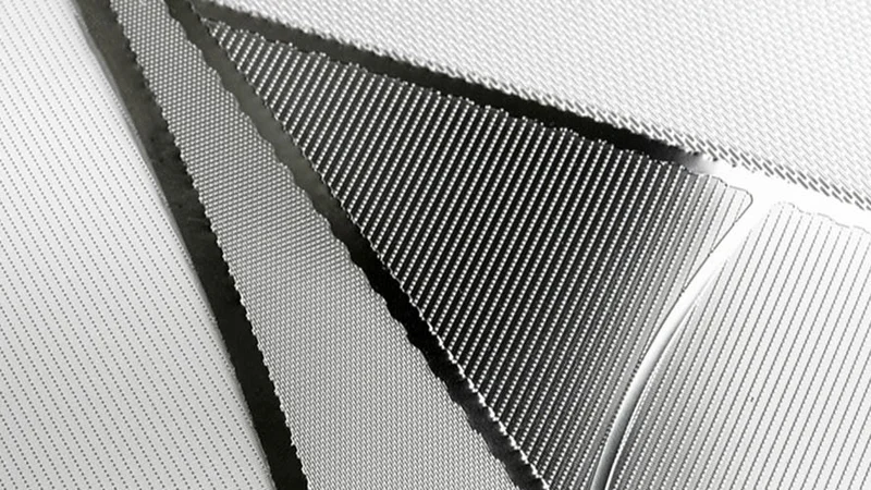
Image credit: Veco
Electroforming has become a game-changing solution for the production of micro-precision products. The technology offers several distinct benefits compared to more traditional manufacturing processes especially when it comes to miniaturization or applications with incredibly tight tolerances. As we’ll see in this article, electroforming is paving the way for innovative next-gen precision engineering applications, including medical nebulizers, filtration solutions, solar cells, and more.
But first, what is electroforming? Electroforming is an additive manufacturing method used for producing micro-precision metal parts with fine features and tight tolerances. The process is unique in its ability to replicate the shape of a mandrel with extreme accuracy and at scalable volumes. Veco's Advanced Lithographic Electroforming process is a unique combination of unparalleled electroforming industry experience, advanced lithography technology and in-depth knowledge of metallurgy.
Capabilities of Electroforming
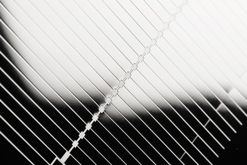
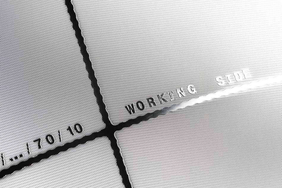
Electroforming unlocks micro-precision capabilities for metal part production by effectively building components atom by atom. The process can achieve tolerances of +/- 1, which is far more precise than most other manufacturing processes. For instance, the typical tolerance of CNC machining is 20 μm.
Not only that, electroforming is also well suited for scalability. The process offers perfect repeatability, which enables customers to easily transition from prototyping to production. It also allows for the simultaneous formation of multiple micro-precision parts at once. In other words, it works well for a range of production volumes.
Below are some of the key benefits offered by the electroforming process:
- Cost efficiency: electroforming is a cost effective process on several levels. For one, the technology does not require a significant equipment investment. The scalable nature of the process also helps to bring down costs associated with transitioning from prototyping to high volume production.
- Short lead times: the mold required for the mandrel takes only hours to produce using the Laser Direct Imager. And electroformed components can typically be manufactured and delivered in four weeks, depending on the complexity of the project.
- Tunable material properties: with electroforming, it is possible to alter material properties of a single material. It is also possible to add various coatings to achieve desired properties, such as anti-corrosion or bio-compatibility.
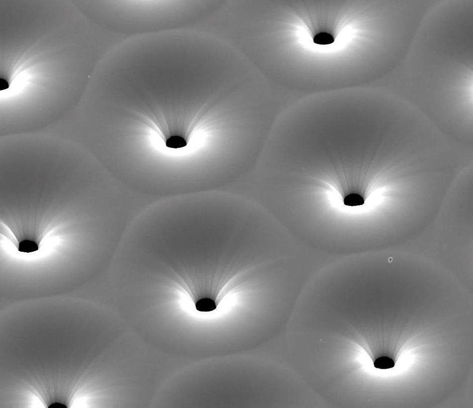
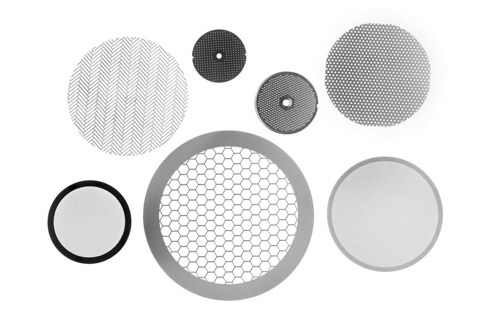
- Freedom of design: electroforming produces parts based on CAD models and is capable of achieving complex geometries with three dimensional features, such as micro-perforations with bell mouth structures.
- Unique features: electroforming is among the best metal production processes for achieving straight wall features that are free from burrs or stress.
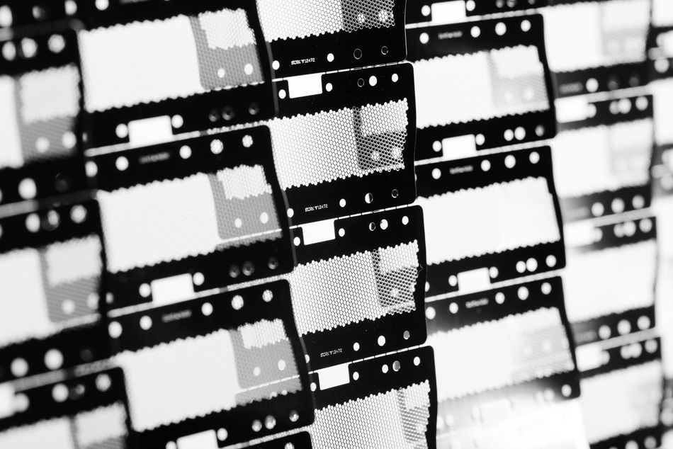
Industry breakthroughs enabled by electroforming
Today, many industries are experiencing the benefits of electroforming first hand, including the aerospace, electronics, food, and medical industries. In fact, the process is creating wholly new opportunities and improving existing applications that take advantage of micro-precision features and geometries. Let’s take a look at some areas where electroforming is proving to be disruptive.
Renewable energy
In recent years, solar energy research groups have turned to electroforming to improve the energy efficiency and cost of solar cells. Specifically, electroforming is used in the production of precision stencils which can be used as an alternative to wire meshes or emulsion screens. The electroformed stencils provide higher energy efficiency at a lower cost. In fact, electroforming specialist Veco and its partner ECN Solar Energy research were awarded at SNEC for their work on next-gen electroformed solar cell printing stencils.
Medical
Electroforming’s ability to produce extremely fine meshes with holes as fine as 2 μm has made it of interest in the medical community, particularly for the production of nebulizer plates. Nebulizers are drug delivery systems that use a combination of micro vibrations and mesh filters to transform liquid medication into a fine mist that can be delivered directly to the lungs. Electroformed nebulizer plates are capable of releasing millions of droplets per second for optimal drug delivery.
Food industry
Electroformed filtration solutions are finding applications in the food manufacturing industry, including in the production of sugar. Necessary in sugar production, electroformed sugar screens are used in continuous centrifuges to separate molasses from sugar crystals. The micro-precision of electroformed sugar screens, made from chrome-plate nickel, enables greater efficiency and ultimately better centrifugal performance for improved sugar yield.
Aerospace
The aerospace industry has benefited hugely from metal additive manufacturing processes, and electroforming is no exception. The process has proven ideal for manufacturing precision filtration screens and orifice plates—used for measuring flow rate—for spacecraft and space instruments. For example, electroformed filters were launched into space in 2006 as part of the Hinode mission. The sieves, produced by Veco, were 18 μm thick and assisted the Hinode spacecraft as it collected data on the Sun’s magnetic fields.
Semiconductor
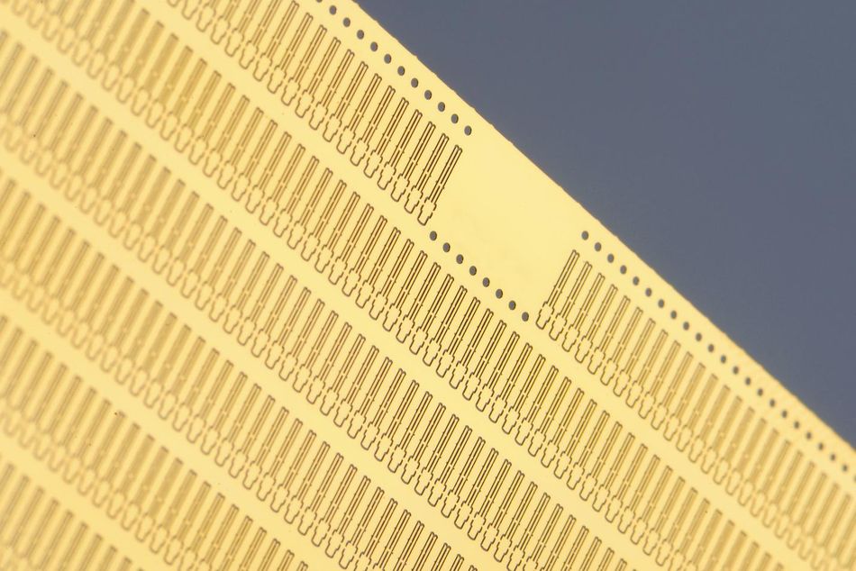
The semiconductor industry is constantly striving to achieve greater miniaturization and increase efficiency and performance. This means semiconductor makers are continually prototyping and testing new products. Electroforming is enabling this ambitious R&D through the production of efficient test contactors. For example, Veco produces precision probes made from Heat Resistant (HR) Nickel for Multitest, a leading manufacturer of semiconductors. The high-precision probes, which are more resistant to the stresses of testing, have improved the reliability, accuracy, and affordability of Multitests’s semiconductor testing process. The electroformed probes can run millions of tests on semiconductors before displaying any signs of wear.
Consumer electronics
If you’ve experienced the smooth close shave of a foil electric shaver, you could have electroforming to thank. The electroforming process can produce shaver foils with incredible precision, resulting in a closer, gentler shave than virtually any other consumer shaving product. Electroforming enables the production of foils with complex patterns, micro-precision features, and ultra-smooth surfaces. Moreover, the electroformed foils are bio-compatible thanks to a combination of high-quality materials and coatings, and have durable, sharp cutting edges.
Co-Development with Veco
Veco is a leader in the world of electroforming and has pioneered its own patented Advanced Lithographic Electroforming technology. The Netherlands-based company is currently involved in all the aforementioned application areas (as well as many others) and works with clients and partners across virtually all industries, including aerospace, automotive, electronics, energy, food, healthcare, industrial automation, printing, and beyond.
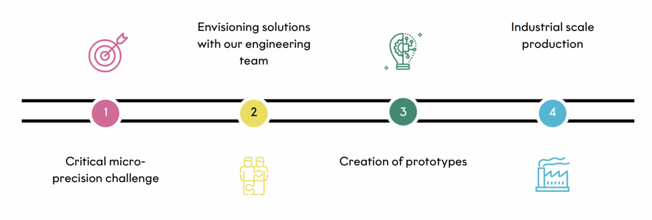
Central to Veco ’s offering is its cooperative ethos. Recognizing that every application and use case has specific needs, the company works closely with its clients to design and develop custom solutions that exploit the benefits of electroforming. Its end-to-end services also go beyond development through to prototyping and ultimately industrial production.