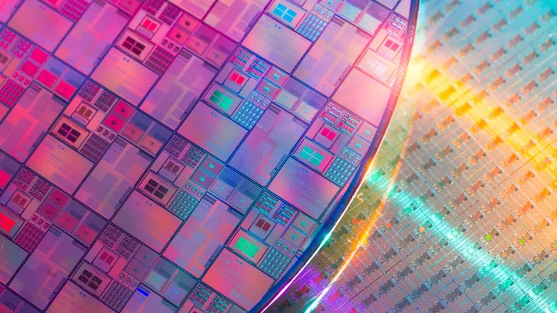
N-Type Vs P-Type: Difference Between P-Type and N-Type Semiconductors
The combination of n-type and p-type semiconductors forms PN junctions, which are essential for the operation of electronic devices. This article explains these vital components and how they pave the way for the electronic devices we rely on every day.

Last updated on 08 Apr, 2024. 28 minutes read
Comparison Chart: What's the difference between p-type and n-type?
For a more simplified representation of the features of the N-type semiconductor VS. P-type semiconductor, the following chart is provided.
Factor of Comparison | P-Type Semiconductor | N-Type Semiconductor |
Group of Doping Element | Group III element is added as a doping element. | Group V element is added as a doping element. |
Effect of Doping Element | Impurity added creates vacancy of electrons (holes) known as Acceptor Atoms. | Impurity added provides extra electrons and is called a Donor Atom. |
Density of Electrons and Holes | The hole density is much higher than the electron density: nh >> ne. | The electron density is much higher than the hole density: ne >> nh. |
Type of impurity added | Trivalent impurity like Al, Ga, In etc. are added. | Pentavalent impurity like P, As, Sb, Bi etc. are added. |
Fermi level | Between acceptor energy level and the valence band, and closer to the valence than conduction band | Between donor energy level and the conduction band, and appears closer to the conduction band than the valence band. |
Energy level | The acceptor energy level is close to the valence band and away from the conduction band. | The donor energy level is close to the conduction band and away from the valence band. |
Movement of Majority carriers | Majority carriers move from higher to lower potential. | Majority carriers move from lower to higher potential |
Majority Carriers | Holes are majority carriers | Electrons are majority carriers |
Minority Carriers | Electrons are minority carriers | Holes are minority carriers |
Introduction: The Essential Duo of Modern Electronics
Semiconductors have revolutionized electronics, enabling devices like smartphones and solar panels. Central to this technology are n-type and p-type semiconductors, which, created through doping, are fundamental to modern electronic devices. N-type semiconductors have an excess of electrons, while p-type semiconductors have an excess of "holes" where an electron could exist.

When n-type and p-type semiconductors meet in a PN junction, they form a boundary where electrons from the n-type region fill the holes in the p-type region, creating a depletion zone. This depletion zone establishes an electric field that allows semiconductor devices to function, such as diodes that allow current flow in one direction and transistors that amplify or switch electronic signals.
While n-type semiconductors can operate independently in certain applications, they are typically used alongside p-type semiconductors in many semiconductor devices. However, in devices involving PN junctions, both n-type and p-type semiconductors are necessary for proper functionality. Understanding the synergy between n-type and p-type semiconductors is crucial for advancing semiconductor technology and developing new electronic devices.
Recommended reading: What is a Semiconductor? A Comprehensive Guide to Engineering Principles and Applications
N-Type Semiconductors: The Electron Donors
N-type semiconductors are materials engineered to exhibit unique electrical properties by introducing specific impurities, or dopants, into the crystal structure. These dopants, typically from group V of the periodic table, such as phosphorus or arsenic, provide extra electrons to the material, significantly altering its electrical characteristics.
The increased electron concentration is a hallmark of n-type semiconductors, enhancing the material's electrical conductivity [8]. These free electrons serve as the primary charge carriers, allowing electric current to flow more easily through the material. Consequently, n-type semiconductors exhibit higher conductivity compared to intrinsic semiconductors.
The presence of extra electrons affects the band structure and Fermi level, shifting the Fermi level closer to the conduction band. This shift occurs because the additional electrons populate energy states near the bottom of the conduction band, reducing the energy gap between the Fermi level and the conduction band edge.
The Fermi level, named after physicist Enrico Fermi, is a concept in solid-state physics that represents the energy level at which electrons in a material have a 50% probability of being occupied at a given temperature. It is a crucial parameter in understanding the electrical properties of materials, especially semiconductors.
Characteristics of N-Type Semiconductors:
Increased electron concentration due to donor impurities
Negative charge carriers (electrons) as the primary means of electrical conduction
Enhanced electrical conductivity compared to intrinsic semiconductors
Fermi level shifted closer to the conduction band
Altered band structure with populated energy states near the conduction band edge
The concentration of dopants in n-type semiconductors can be precisely controlled during manufacturing to fine-tune the material's electrical properties. Careful optimization is necessary to achieve the desired balance between conductivity and other performance parameters.
Common N-Type Dopants and Their Effects
Phosphorus is a widely favored choice for doping n-type silicon semiconductors, including those used in n-type solar panels and n-type solar cells. When phosphorus atoms replace silicon atoms in the crystal lattice, they create four covalent bonds with neighboring silicon atoms. However, phosphorus has one more valence electron than silicon, making it an effective donor. This extra electron can easily move into the conduction band, increasing electron concentration and boosting electrical conductivity. Phosphorus-doped silicon can achieve a solubility limit of about 1.5 × 10^21 atoms/cm^3 at 1100°C, offering flexibility in doping concentrations for various applications.
Another popular n-type dopant is arsenic, particularly favored for high-performance semiconductor devices. Like phosphorus, arsenic has five valence electrons, enabling it to donate an extra electron to the conduction band when incorporated into the semiconductor lattice. Arsenic-doped semiconductors often exhibit higher electron mobility, making them suitable for applications requiring fast switching speeds or high-frequency operation. The solubility limit of arsenic in silicon is similar to that of phosphorus, around 1.7 × 10^21 atoms/cm^3 at 1100°C.
Antimony is also used as an n-type dopant, although less frequently than phosphorus and arsenic. Like other group V elements, antimony has five valence electrons and can contribute extra electrons to the semiconductor lattice. However, antimony's larger atomic radius compared to phosphorus and arsenic can introduce more significant lattice strain, impacting the material's structural properties. The solubility limit of antimony in silicon is lower, approximately 7 × 10^20 atoms/cm^3 at 1100°C.
The following table compares the key properties of phosphorus, arsenic, and antimony as n-type dopants:
Dopant | Atomic Number | Valence Electrons | Ionization Energy (eV) | Electron Mobility (cm^2/Vs) | Solubility Limit in Silicon (atoms/cm^3) at 1100°C |
Phosphorus | 15 | 5 | 0.044 | 1500 | 1.5 × 10^21 |
Arsenic | 33 | 5 | 0.054 | 1200 | 1.7 × 10^21 |
Antimony | 51 | 5 | 0.039 | 500 | 7 × 10^20 |
The choice of n-type dopant depends on factors like desired electrical properties, semiconductor material, and application needs. Phosphorus and arsenic are popular due to their favorable electrical characteristics, compatibility with silicon, and high solubility limits. The solubility limit determines the maximum dopant concentration without causing crystal defects. Controlling dopant concentration within these limits allows tailoring of n-type semiconductor properties for various electronic devices.
Advanced Doping Techniques for N-Type Semiconductors
As the semiconductor industry continues to push the boundaries of device performance and miniaturization, advanced doping techniques have emerged to address the limitations of traditional doping methods. One such technique is atomic layer doping (ALD), which offers unparalleled control over dopant distribution and concentration in n-type semiconductors.
In traditional doping methods like ion implantation or diffusion, dopants are introduced into semiconductor material through high-energy particle bombardment or thermal diffusion. These methods often result in non-uniform dopant profiles and can cause crystal damage, impacting device performance.
Atomic layer doping, however, uses atomic layer deposition to achieve precise and conformal doping profiles. This process exposes the semiconductor surface to alternating pulses of dopant precursors and reactants, chemically reacting with the surface in a self-limiting manner. Each ALD cycle deposits a single atomic layer of the dopant material, allowing for precise control over dopant concentration and distribution. Common dopant precursors for ALD include phosphine (PH3) and arsine (AsH3) for n-type doping of silicon.
One of the key advantages of atomic layer doping is its ability to achieve ultra-shallow and abrupt doping profiles. By carefully controlling the number of ALD cycles, engineers can tailor the dopant concentration with atomic-scale precision, enabling the fabrication of advanced device structures such as ultra-shallow junctions and delta-doped layers. For example, ALD has been used to create phosphorus-doped silicon layers with a dopant concentration of 10^21 atoms/cm^3 and a junction depth of less than 5 nm, which is crucial for maintaining the performance and reliability of increasingly miniaturized semiconductor devices.
Furthermore, atomic layer doping can create conformal doping profiles on intricate three-dimensional structures, like FinFETs and nanowires. Traditional methods often struggle with uniform doping on such structures, affecting device performance. ALD's ability to deposit dopants uniformly on complex surfaces addresses this, ensuring consistent doping throughout the device. This capability is evident in the production of phosphorus-doped silicon FinFETs with 5 nm fin widths, highlighting ALD's potential in advanced device design.
Atomic layer doping (ALD) offers precise control over dopant placement in semiconductors, leading to significant improvements. Compared to traditional methods, ALD-doped devices boast better performance due to minimized crystal damage and optimal dopant profiles. Studies show that ALD-doped transistors can achieve a 50% increase in electron mobility and a 10x reduction in leakage current, showcasing its potential for n-type semiconductor advancement.
P-Type Semiconductors: The Hole Providers
P-type semiconductors are a fundamental building block of modern electronics. They are created by introducing specific impurities, called acceptor dopants, into the crystal structure of an intrinsic semiconductor. These dopants, typically elements from Group III of the periodic table (like boron, aluminum, or gallium), have a significant impact on the electrical properties of the material.
Acceptor dopants have one fewer valence electrons compared to the host semiconductor atoms (like silicon). When incorporated into the lattice, they create "holes" within the crystal structure. Imagine a vacancy where an electron should be - this vacancy acts as a positive charge carrier. In simpler terms, the dopant "borrows" an electron from a neighboring atom, leaving behind a hole that can move freely.
The presence of these holes alters the internal energy distribution of the semiconductor, represented by its band structure and Fermi level [9]. In an intrinsic semiconductor, the Fermi level sits roughly in the middle. However, p-type doping introduces energy states near the top of the valence band, readily occupied by electrons, creating more holes. This shift in the Fermi level reflects the increased number of holes compared to electrons.
Key Characteristics of P-Type Semiconductors
High Hole Concentration: P-type semiconductors boast a significant increase in hole concentration (typically 10^15 to 10^20 cm^-3) compared to intrinsic materials.
Dominant Positive Charge Carriers: Holes become the primary means of electrical conduction in p-type semiconductors, although their mobility (ease of movement) is generally lower than electrons in n-type counterparts.
Enhanced Conductivity: Doping leads to increased electrical conductivity compared to intrinsic semiconductors, with the exact value depending on dopant concentration and temperature.
Shifted Fermi Level: As mentioned earlier, the Fermi level moves closer to the valence band, reflecting the dominance of holes.
Tailored Band Structure: P-type doping creates empty energy states near the valence band, facilitating efficient hole movement.
Careful control of dopant type and concentration allows engineers to tailor p-type semiconductors for specific applications. This manipulation of electrical properties, a direct result of doping, has driven innovation in countless electronic devices, shaping modern technology. The unique dominance of holes in p-type semiconductors makes them essential components for various electronic functions.
Recommended reading: Semiconductor Fabrication Process: The Ultimate Guide to Creating Cutting-Edge Electronics
Common P-Type Dopants and Their Effects
Elements like boron (B), aluminum (Al), and gallium (Ga) from Group III act as common p-type dopants in semiconductors. These "acceptor impurities" introduce holes, altering electrical properties.
Boron is a popular choice for creating p-type silicon semiconductors. When incorporated into the silicon lattice, boron atoms, with only three valence electrons, "borrow" an electron from a neighboring silicon atom (having four). This creates a "hole" in the valence band, acting as a positive charge carrier and boosting conductivity. The concentration of these holes can range from 10^15 to 10^20 cm^-3, depending on the doping level. However, excessively high doping (above 10^19 cm^-3) can hinder hole mobility due to increased scattering.
Similar to boron, aluminum (with three valence electrons) acts as a p-type dopant in compound semiconductors like gallium arsenide (GaAs) and indium phosphide (InP). This creates holes, boosting conductivity. Hole mobility varies (100-400 cm^2/Vs) depending on the material and doping level. Notably, aluminum in GaAs has a high solubility limit (10^20 atoms/cm^3), allowing for wider doping control.
Gallium (Ga), another Group III element with three valence electrons, plays a key role as a p-type dopant in various semiconductors. When incorporated into the crystal lattice, gallium atoms introduce "holes," leading to increased hole concentration and enhanced electrical conductivity. This tailored electrical property makes gallium-doped materials like gallium nitride (GaN) and gallium phosphide (GaP) highly suitable for applications in light-emitting diodes (LEDs), laser diodes, and even high-speed electronic devices. Notably, the mobility of these holes can vary significantly (10-400 cm^2/Vs) depending on the specific material and doping level.
The following table compares the key properties of boron, aluminum, and gallium as p-type dopants:
Dopant | Atomic Number | Valence Electrons | Ionization Energy (eV) | Hole Mobility (cm^2/Vs) | Solubility Limit in Silicon (atoms/cm^3) at 1100°C |
Boron | 5 | 3 | 0.045 | 450 | 2.4 × 10^20 |
Aluminum | 13 | 3 | 0.067 | 200 | 2.0 × 10^19 |
Gallium | 31 | 3 | 0.072 | 250 | 4.5 × 10^19 |
Choosing the Right P-Type Dopant
The ideal p-type dopant depends on several factors:
Semiconductor Material: Different materials (e.g., silicon vs. gallium arsenide) favor specific dopants for efficient integration and hole generation.
Electrical Properties: Boron, with its high solubility in silicon, is popular for achieving desired conductivity levels.
Application Needs: Aluminum and gallium offer good control over hole concentration in compound semiconductors, crucial for devices like LEDs.
Higher dopant concentration usually translates to increased conductivity, but too much can backfire. Excessive dopants can hinder hole mobility due to scattering, impacting device performance. Therefore, engineers carefully optimize the dopant concentration to achieve the ideal balance between conductivity and mobility in p-type semiconductors.
Advanced Doping Techniques for P-Type Semiconductors
As the need for ever more precise control over electrical properties grows, the semiconductor industry is embracing advanced doping techniques like plasma doping (PIII). This method offers a significant advantage over traditional methods by enabling the creation of highly customized dopant profiles in p-type semiconductors.
In plasma doping, the semiconductor wafer is exposed to a plasma containing the desired dopant species, such as boron or aluminum. The plasma is generated by applying a high-voltage pulse to a gas mixture, which ionizes the dopant atoms and accelerates them toward the wafer surface. As the ions impact the surface, they penetrate the semiconductor lattice and come to rest at a specific depth, determined by their energy and the properties of the target material. The ion energy in plasma doping can range from a few hundred electron volts to several kilo electron volts, allowing for precise control over the implantation depth and dopant profile.
Plasma doping shines in its ability to create incredibly precise "dopant profiles." Imagine placing dopant atoms at specific depths within the material, like microscopic architects. This fine-tuning allows engineers to tailor electrical properties for optimal device performance. Plasma doping excels at achieving ultra-shallow junctions (less than 10 nm deep) with high dopant concentrations (over 10^20 cm^-3) – crucial for high-performance transistors and other tiny devices. Traditional methods struggle with such precision, making plasma doping a game-changer for advanced device architectures.
Another strength of plasma doping is its ability to coat complex 3D structures like fins and nanowires uniformly. Traditional methods have trouble reaching all the nooks and crannies due to limitations in how they aim the dopant atoms. Plasma doping, on the other hand, acts like a magical spray paint, reaching every corner and ensuring even distribution of dopants throughout the device. This "conformal doping" is crucial for the next generation of 3D devices, where consistent doping is essential for top performance and reliability.
Beyond its precision, plasma doping boasts economic advantages. It processes multiple wafers at once, significantly speeding up production. Additionally, these systems require less maintenance and have lower running costs compared to traditional methods. This translates to a double win for manufacturers: faster production times and lower overall costs. In the competitive world of semiconductors, where efficiency is key, these economic benefits make plasma doping a highly attractive option.
The precise control offered by plasma doping translates directly to better performance in p-type semiconductor devices. This is because optimized dopant profiles lead to several improvements:
Enhanced Carrier Mobility: Dopants act like highways for charge carriers within the material. Precise placement improves their movement, leading to more efficient current flow.
Reduced Series Resistance: Imagine electrical resistance as roadblocks that slow down current. Plasma doping minimizes these roadblocks, allowing for smoother current flow and improved device performance.
Overall Performance Boost: The combined effect of these improvements is a significant increase in overall device performance compared to traditionally doped devices. For instance, studies show a 20% jump in conversion efficiency for plasma-doped solar cells.
While plasma doping offers significant advantages, it's not without hurdles. The intense plasma can damage the delicate semiconductor surface and introduce imperfections. To overcome this, engineers have to fine-tune the plasma settings like energy and density to minimize harm while achieving the desired dopant profile. Additionally, researchers are developing advanced surface protection techniques like ultra-thin dielectric layers or atomic layer deposited coatings. These act like microscopic shields, safeguarding the surface during the doping process and ensuring optimal device performance.
Another challenge associated with plasma doping is the need for precise control over the plasma uniformity and ion energy distribution. Non-uniformities in the plasma can lead to variations in dopant concentration across the wafer, while a broad ion energy distribution can result in a wider range of implantation depths and potential damage to the semiconductor lattice.
To address these challenges, advanced plasma doping systems employ techniques such as plasma confinement, magnetic field control, and ion energy filtering to improve plasma uniformity and narrow the ion energy distribution. For example, the use of a multi-grid ion energy filter can help to reduce the energy spread of the ions reaching the wafer surface, enabling more precise control over the dopant profile and minimizing lattice damage.
Recommended reading: Wafer Thinning: Investigating an essential part of semiconductor fabrication
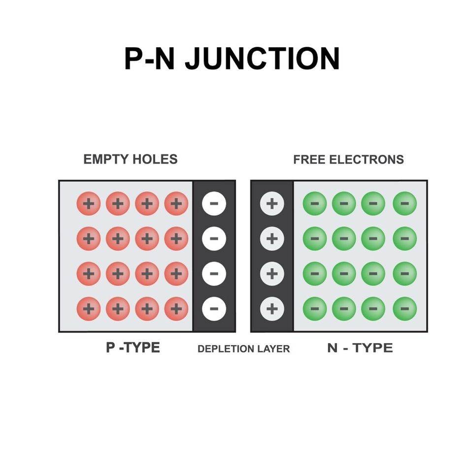
The PN Junction: Where N-Type and P-Type Semiconductors Meet
A PN junction is a fundamental building block of semiconductor devices, formed by bringing together n-type and p-type semiconductors in close contact. The creation of a PN junction is a crucial step in the fabrication of diodes, solar cells, LEDs, and many other electronic components. Understanding the formation and structure of PN junctions is essential for designing and optimizing semiconductor devices with desired electrical properties.
Formation and Structure of PN Junctions
Initially, the concentration gradient of electrons and holes across the junction causes diffusion current to flow. Electrons from the n-type region diffuse into the p-type region, while holes from the p-type region diffuse into the n-type region. As the carriers diffuse, they leave behind ionized dopant atoms near the junction, creating a region depleted of mobile charge carriers known as the depletion region or space charge region.
The ionized dopant atoms in the depletion region give rise to a built-in electric field that opposes the diffusion current. The electric field sweeps the mobile charge carriers away from the junction, causing a drift current in the opposite direction of the diffusion current. At equilibrium, the diffusion current and drift current balance each other, resulting in a net current of zero across the PN junction. The equilibrium condition is characterized by a built-in potential difference across the depletion region, typically ranging from 0.5 to 1.0 V, depending on the semiconductor materials and doping concentrations. The built-in potential can be calculated using the following equation:
V_bi = (kT/q) * ln(N_A * N_D / n_i^2)
where V_bi is the built-in potential, k is the Boltzmann constant, T is the absolute temperature, q is the elementary charge, N_A, and N_D are the acceptor and donor doping concentrations, respectively, and n_i is the intrinsic carrier concentration of the semiconductor material.
The width of the depletion region depends on various factors, such as the doping concentrations of the n-type and p-type regions, the applied voltage, and the temperature. In general, the depletion region extends more into the lightly doped side of the junction due to the lower concentration of ionized dopant atoms. The width of the depletion region can be controlled by applying an external voltage across the PN junction, which alters the balance between the diffusion and drift currents. The depletion region width can be calculated using the following equation:
W_D = sqrt(2 * ε_s * (V_bi - V_a) * (N_A + N_D) / (q * N_A * N_D))
where W_D is the depletion region width, ε_s is the permittivity of the semiconductor material, V_a is the applied voltage, and the other symbols have the same meaning as in the previous equation.
Advanced PN Junction Structures
Heterojunctions and quantum wells are advanced PN junction structures that have revolutionized semiconductor devices, particularly in the realm of solar energy. These structures offer unique properties and enhanced functionality, enabling the creation of novel devices with improved efficiency, speed, and versatility.
Heterojunctions, for instance, are formed by combining two dissimilar semiconductor materials with different bandgaps, creating a PN junction at their interface. This allows for the engineering of the band structure and the control of charge carrier flow across the junction. By carefully selecting the semiconductor materials and optimizing their properties, engineers can design heterojunctions with tailored electrical and optical characteristics. Heterojunctions also help reduce the impact of surface states and defects by confining charge carriers away from the surface and into the bulk of the device.
On the other hand, quantum wells are thin layers of semiconductor material sandwiched between two layers of a wider bandgap material. This creates a potential well that confines the charge carriers in one dimension, leading to the quantization of their energy levels and resulting in unique optical and electrical properties. Quantum wells have revolutionized the development of high-efficiency light-emitting diodes (LEDs) and laser diodes by enabling higher radiative recombination rates and improved efficiency. The use of multiple quantum wells (MQWs) further enhances the performance of these devices by increasing the volume of the active region and allowing for the optimization of carrier injection and confinement.
In the realm of solar energy, advanced PN junction structures play a crucial role. Heterojunction solar cells, for example, combine a crystalline silicon substrate with thin layers of amorphous silicon or other wide-bandgap materials. These cells have demonstrated efficiencies exceeding 26% in laboratory settings. The heterojunction structure helps to passivate the surface of the crystalline silicon, reducing recombination losses and enhancing the collection of photogenerated charge carriers. Similarly, n-type solar panels, which incorporate n-type solar cells, have shown promise in enhancing solar energy conversion efficiency.
Quantum well solar cells, though less mature, offer the potential for even higher efficiencies by exploiting the unique properties of quantum-confined structures. By stacking multiple quantum wells with different bandgaps, engineers can create multi-junction solar cells that can absorb a wider range of the solar spectrum, potentially achieving efficiencies beyond the Shockley-Queisser limit for single-junction cells. Both n-type and p-type solar panels, leveraging their respective properties, contribute to the advancement of solar energy technology.
The integration of these advanced structures into solar panels and cells has the potential to significantly improve solar energy conversion efficiency. Light-induced degradation, a common issue in solar panels, can be mitigated through the use of these advanced structures, ensuring long-term performance and reliability. Overall, the development and optimization of these advanced PN junction structures are crucial for the continued advancement of solar energy technology, offering a path towards more efficient and sustainable energy generation.
Real-World Applications of N-Type and P-Type Semiconductors
N-type and P-type semiconductors play vital roles in electronic devices. N-type semiconductors excel in applications requiring efficient electron flow, like transistors and diodes. They're also key in photovoltaic cells, converting light energy into electricity effectively. P-type semiconductors are crucial for devices like solar cells, where hole movement generates current. They're also used in diodes and transistors needing controlled current flow.
Transistors: The Building Blocks of Modern Electronics
Transistors, the fundamental building blocks of modern electronic circuits, enable the amplification, switching, and processing of electrical signals. These semiconductor devices have revolutionized electronics, paving the way for compact, high-performance, and energy-efficient systems. Transistors leverage the unique properties of n-type and p-type semiconductors to create two main types: bipolar junction transistors (BJTs) and field-effect transistors (FETs).
BJTs are formed by sandwiching a thin layer of one type of semiconductor between two layers of the opposite type, creating an emitter, base, and collector. In an NPN BJT, the emitter and collector are n-type, while the base is p-type. In a PNP BJT, the emitter and collector are p-type, and the base is n-type. The base-emitter voltage controls the current flow from the emitter to the collector, making BJTs suitable for high-output current applications like power amplifiers and switching regulators.
FETs, on the other hand, use an electric field to control the current flow through the device. JFETs have a channel of n-type or p-type semiconductor material sandwiched between two gate regions of the opposite type. The gate voltage modulates the channel conductivity by creating a depletion region. MOSFETs, the most common transistor in integrated circuits, use a metal gate electrode insulated from the semiconductor channel by a thin oxide layer. The gate voltage controls the formation of an inversion layer in the channel, allowing current to flow between the source and drain. MOSFETs are preferred for their high input impedance, low power consumption, and scalability, making them ideal for digital logic circuits and memory devices.
Transistor amplifiers, like the common-emitter amplifier, increase the amplitude of electrical signals. The voltage gain (A_v) of a common-emitter amplifier is given by:
A_v = -R_C / R_E
where R_C is the collector resistor and R_E is the emitter resistor. The negative sign indicates a 180-degree phase shift between input and output. Voltage gains of 50 or more are possible, but the amplifier's bandwidth is limited by the transistor's gain-bandwidth product (GBP). A transistor with a GBP of 100 MHz and a voltage gain of 50 would have a maximum operating frequency of 2 MHz.
Transistors also implement logic gates, the building blocks of digital circuits. MOSFET-based CMOS circuits offer low power consumption, high noise immunity, and good scalability. A CMOS NAND gate consists of two n-type MOSFETs in series and two p-type MOSFETs in parallel. When both inputs are high, the n-type MOSFETs pull the output low (0). Otherwise, at least one p-type MOSFET pulls the output high (1). The propagation delay of a CMOS NAND gate is typically tens of picoseconds, depending on the technology node and load capacitance.
Transistor performance is determined by key parameters like current gain (β), transconductance (g_m), and cutoff frequency (f_T). Higher current gains allow for greater amplification and reduced power consumption. Higher transconductance enables faster switching and higher operating frequencies. The cutoff frequency sets the upper limit for the transistor's operating frequency. Modern high-frequency transistors, such as HBTs and HEMTs, can achieve cutoff frequencies exceeding 100 GHz, enabling applications in RF and millimeter-wave circuits.
As the demand for faster, more efficient, and more compact electronic devices grows, advanced transistor technologies are being developed. Researchers are exploring new materials, device architectures, and fabrication techniques to overcome the limitations of conventional silicon-based transistors. Compound semiconductors like GaAs and InP offer higher electron mobility and better high-frequency performance than silicon. Emerging technologies, such as carbon nanotube transistors and quantum dot transistors, have the potential to enable ultra-small, ultra-fast, and ultra-low-power devices that could outperform conventional transistors in terms of speed, efficiency, and functionality.
Emerging Applications: Spintronics and Topological Insulators
As the demand for faster, more efficient, and more compact electronic devices continues to grow, researchers are exploring new materials and phenomena that could revolutionize the field of semiconductors. Two emerging areas that have garnered significant attention in recent years are spintronics and topological insulators. These materials and devices exploit the unique properties of electrons, such as their spin and topology, to enable novel functionalities and overcome the limitations of conventional semiconductor technologies.
Spintronics, or spin electronics, is an emerging field that utilizes the spin of electrons, in addition to their charge, for information processing and storage. In conventional electronics, the flow of electrical charge is used to represent and manipulate information. However, in spintronics, the spin state of electrons is employed as an additional degree of freedom, allowing for the development of novel devices with enhanced performance and functionality. The key advantage of spintronics is the ability to combine the processing and storage of information in a single device, potentially leading to faster, more energy-efficient, and more compact electronic systems.
One of the most promising materials for spintronics applications is gallium manganese arsenide (GaMnAs), a dilute magnetic semiconductor. In GaMnAs, a small fraction of the gallium atoms is replaced by manganese, which introduces magnetic moments into the semiconductor lattice. The interaction between the magnetic moments and the spins of the electrons leads to a phenomenon called carrier-mediated ferromagnetism, where the material becomes ferromagnetic at low temperatures. This unique property allows for the control of the magnetic state of the material using electrical fields, enabling the development of spintronic devices such as spin transistors, spin valves, and spin-based logic circuits.
Another material system that has shown great potential for spintronics is the topological insulator, a class of materials that exhibit unique electronic properties due to their topology. Topological insulators are characterized by insulating bulk and conducting surface states that are protected by time-reversal symmetry. These surface states have a special property called spin-momentum locking, where the spin of the electrons is locked perpendicular to their momentum. This property enables the generation and manipulation of spin-polarized currents without the need for external magnetic fields, making topological insulators promising candidates for spintronic devices.
One of the most well-studied topological insulators is bismuth selenide (Bi2Se3), which has a large bandgap in the bulk and a single Dirac cone on the surface. The surface states of Bi2Se3 have been experimentally observed using angle-resolved photoemission spectroscopy (ARPES) and scanning tunneling microscopy (STM), confirming the presence of spin-momentum locking. Researchers have demonstrated the ability to control the spin polarization of the surface states using electrical gates, paving the way for the development of topological insulator-based spintronic devices such as spin-orbit torque switches and spin-based memory cells.
The integration of spintronic materials and topological insulators into existing semiconductor technologies presents both challenges and opportunities. One of the main challenges is the growth and fabrication of these materials, which often require precise control over the composition, thickness, and interface quality. For example, the growth of high-quality GaMnAs films requires low-temperature molecular beam epitaxy (MBE) to prevent the formation of secondary phases and maintain the ferromagnetic properties of the material. Similarly, the growth of topological insulators requires careful control over the stoichiometry and the substrate temperature to ensure the formation of the desired crystal structure and electronic properties.
Another challenge is the integration of these materials with conventional semiconductor devices and circuits. The different crystal structures, lattice constants, and thermal expansion coefficients of spintronic materials and topological insulators compared to silicon can lead to strain, defects, and interface states that degrade the performance of the devices. To overcome these challenges, researchers are developing advanced growth techniques, such as metamorphic buffer layers and selective area growth, to enable the integration of these materials on silicon substrates. Additionally, novel device architectures, such as vertical spintronic devices and topological insulator-based heterostructures, are being explored to optimize the performance and functionality of these devices.
Despite these challenges, the unique properties of spintronic materials and topological insulators offer tremendous opportunities for the development of novel electronic devices and systems. For example, spintronic devices based on GaMnAs have the potential to enable high-density, non-volatile memory cells that combine the advantages of DRAM and flash memory, such as fast read/write speeds and long data retention times. Similarly, topological insulator-based devices could enable the development of ultra-low-power and high-speed spintronic logic circuits that operate at room temperature, overcoming the limitations of current CMOS technology.
Moreover, the combination of spintronics and topological insulators with other emerging technologies, such as superconductors and quantum computing, could lead to even more exciting possibilities. For instance, the integration of topological insulators with superconductors could enable the realization of Majorana fermions, exotic particles that could be used for fault-tolerant quantum computing. The development of spintronic qubits based on GaMnAs or topological insulators could also provide a scalable platform for quantum information processing, complementing the efforts in other qubit technologies such as superconducting qubits and trapped ions.
As research into spintronics and topological insulators continues to advance, we can expect to see further breakthroughs in the understanding and control of these materials, as well as the development of novel device concepts and architectures. The successful integration of these materials into existing semiconductor technologies could lead to a new generation of electronic devices with enhanced performance, functionality, and energy efficiency. However, realizing this potential will require a concerted effort from the research community, industry, and policymakers to address the scientific, technological, and economic challenges associated with these emerging technologies.
Challenges and Considerations in Semiconductor Engineering
Semiconductor engineering faces numerous challenges and considerations. Shrinking transistor sizes, increased power density, and thermal management are critical issues. Additionally, ensuring reliability, scalability, and compatibility with emerging technologies are ongoing concerns. Below are some major challenges:
Fabrication Techniques and Limitations
The fabrication of n-type and p-type semiconductors involves techniques such as ion implantation and diffusion, which enable precise control of dopant concentration, distribution, and activation. However, each technique comes with its own set of challenges and limitations that must be addressed to ensure optimal device performance and reliability.
Ion implantation is widely used for introducing dopants into semiconductors. In this process, dopant ions are accelerated to high energies (10-500 keV) and directed towards the semiconductor surface. The depth profile of the implanted ions depends on factors such as ion energy, mass, and target material properties. Ion implantation offers high spatial resolution and uniformity, enabling the fabrication of ultra-shallow junctions and highly doped regions with nanoscale precision. However, high-energy ions can cause lattice damage, creating defects that degrade electrical properties, leading to reduced carrier mobility, increased leakage current, and poor device performance.
To mitigate implantation-induced damage, post-implantation annealing is performed. The semiconductor wafer is heated to high temperatures (600-1200°C) for a specific duration to repair lattice damage and activate implanted dopants. Annealing conditions must be optimized to maintain the desired dopant profile while minimizing dopant diffusion and secondary defect formation.
Diffusion is another common technique for introducing dopants into semiconductors. The semiconductor wafer is exposed to a dopant source at elevated temperatures, allowing dopant atoms to diffuse into the material driven by concentration gradient and thermal energy. The diffusion profile depends on temperature, time, and properties of the dopant and host material. Diffusion offers a simpler and less damaging approach compared to ion implantation. However, it is isotropic, making it challenging to achieve precise control over the dopant profile. High temperatures required for diffusion can also lead to the redistribution of previously introduced dopants and the formation of unwanted compounds or phases.
Advanced diffusion techniques, such as rapid thermal processing (RTP) and laser annealing, have been developed to overcome these limitations. RTP uses high-intensity lamps or lasers to heat the wafer to high temperatures for short durations, enabling rapid diffusion and activation of dopants while minimizing thermal budget. Laser annealing uses focused laser beams to melt and recrystallize the semiconductor surface, allowing for dopant incorporation and lattice damage repair with minimal diffusion.
Key fabrication steps for creating n-type and p-type semiconductors using ion implantation and diffusion:
Surface preparation: Wafer cleaning and preparation for doping, which may involve oxide growth or mask material deposition to define doping regions.
Ion implantation: Dopant ion acceleration and implantation into the semiconductor surface, with controlled ion energy, dose, and angle to achieve the desired dopant profile. Challenges include ensuring uniform dopant distribution, minimizing lattice damage, and preventing contamination.
Post-implantation annealing: Heating the implanted wafer to high temperatures to repair lattice damage and activate dopants. Optimizing annealing conditions is crucial to achieve the desired dopant profile and minimize diffusion. Challenges include controlling the thermal budget, preventing dopant loss or redistribution, and avoiding secondary defect formation.
Diffusion: Exposing the wafer to a dopant source at elevated temperatures to allow dopant diffusion into the material. Diffusion conditions (temperature, time, and dopant source) are controlled to achieve the desired dopant profile. Challenges include achieving uniform and reproducible doping, minimizing the thermal budget, and preventing the formation of unwanted compounds or phases.
Post-diffusion processing: Additional steps such as dopant source removal, capping layer growth, or electrical contact formation. Challenges include maintaining dopant profile integrity, minimizing contamination, and ensuring compatibility with subsequent device fabrication steps.
Process parameters significantly impact device performance. In ion implantation, ion energy determines the implantation depth, while dose determines the dopant concentration. Higher energies result in deeper implantation but increase the risk of lattice damage. Higher doses lead to higher concentrations but also increase the risk of defect formation. In diffusion, temperature and time determine the extent and profile of dopant diffusion. Higher temperatures and longer times result in deeper and more uniform profiles but increase the risk of dopant redistribution and unwanted compound formation.
For example, in the fabrication of an n-type MOSFET, source and drain regions are typically formed by ion implantation of arsenic or phosphorus, with doses of 10^15 to 10^16 cm^-2 and energies of 10 to 100 keV. Increasing the implantation energy from 30 keV to 50 keV can increase the junction depth from 50 nm to 100 nm, reducing short-channel effects but increasing parasitic resistance. Increasing the dose from 5x10^15 cm^-2 to 1x10^16 cm^-2 can increase the peak dopant concentration from 1x10^20 cm^-3 to 2x10^20 cm^-3, reducing threshold voltage but increasing off-state leakage current.
Achieving optimal device performance requires careful tuning and optimization of implantation and diffusion conditions based on specific device requirements and material properties. This involves extensive process simulations, design of experiments, and characterization techniques to understand the complex interplay between process parameters and device characteristics.
Advanced Characterization Techniques for Quality Control
Advanced characterization techniques are essential for ensuring the quality, reliability, and performance of semiconductor devices. These techniques detect and analyze defects, impurities, and structural properties of semiconductor materials during manufacturing. Electron microscopy and X-ray diffraction are two widely used techniques in semiconductor manufacturing.
Electron microscopy, including scanning electron microscopy (SEM) and transmission electron microscopy (TEM), offers high-resolution imaging and analysis of semiconductor materials and devices. SEM scans the sample surface with a focused electron beam, generating secondary electrons to form an image. It can resolve features down to a few nanometers, inspecting surface morphology, defects, and contamination. TEM passes a high-energy electron beam through a thin sample, providing information about its internal structure, crystallinity, and composition at an atomic scale.
These microscopy techniques are crucial for detecting and analyzing defects like dislocations and stacking faults in semiconductor materials. For instance, in epitaxial layer fabrication, TEM can characterize the interface between the layer and substrate, revealing misfit dislocations or strain-induced defects to optimize growth conditions.
X-ray diffraction (XRD) is another important technique, relying on X-ray interactions with the atomic structure of a crystalline material to reveal its crystal structure, lattice parameters, strain, and composition. In device fabrication, XRD characterizes the crystalline quality of epitaxial layers, monitors strain in heterostructures, and detects unwanted phases or impurities.
High-resolution XRD (HRXRD) measures epitaxial layer composition and thickness precisely. By analyzing diffraction peaks, engineers determine lattice mismatch between layers, crucial for controlling strain and preventing defect formation. HRXRD also detects unwanted phases, like oxides or silicides, which can degrade device performance.
These techniques are critical for ensuring device reliability and performance. By providing detailed structural and compositional information, engineers can identify issues and optimize fabrication processes. In power electronic device manufacturing, defects or impurities can cause premature failure or reduced performance. Electron microscopy and XRD characterize material quality, helping engineers identify and mitigate these issues.
Data from these techniques optimizes fabrication processes and improves device yield. In CMOS device fabrication, for example, TEM characterizes dopant distribution and activation in source and drain regions, enabling engineers to fine-tune implantation and annealing conditions for desired junction depth and electrical properties. XRD data optimizes epitaxial layer growth conditions to minimize defects and achieve high-quality material.
In addition to electron microscopy and XRD, other advanced characterization techniques used in semiconductor manufacturing include:
Secondary ion mass spectrometry (SIMS): Measures the concentration and distribution of dopants and impurities in semiconductor materials with sub-nanometer resolution.
Atomic force microscopy (AFM): Maps the surface topography of a sample with nanometer-scale resolution, characterizing surface roughness, step heights, and morphology of various layers and structures.
Raman spectroscopy: A non-destructive technique that uses inelastic scattering of light to probe the vibrational and structural properties of materials, characterizing stress, composition, and crystalline quality of epitaxial layers and device structures.
Advanced characterization techniques are crucial in semiconductor manufacturing for developing cutting-edge devices and ensuring high yield and reliability. As devices shrink and new materials are used, these techniques play a critical role in quality control and process optimization. The industry invests in new techniques, like machine learning for defect detection and in-line monitoring for real-time process control.
Conclusion
N-type and p-type semiconductors, distinguished by their dopants and resulting charge carriers, are the workhorses of modern electronics. Their unique properties form the foundation for a vast array of devices, from everyday transistors to cutting-edge solar cells.
By mastering the art of doping and understanding these materials' characteristics, engineers can tailor semiconductors for specific needs. This allows for the creation of efficient solar cells, powerful processors, and advanced sensors that shape our world.
As the demand for smaller, faster, and more efficient electronics intensifies, the importance of semiconductor research grows ever stronger. Engineers and researchers will continue to explore new materials, device designs, and fabrication techniques, pushing the boundaries of what's possible.
This journey requires a deep understanding of n-type and p-type semiconductors, the bedrock of this technology. It's a field brimming with potential, fueled by discoveries like novel materials and innovative device concepts. As we delve deeper into this fascinating world, we can expect even more remarkable electronic devices and systems to emerge, transforming our lives in exciting ways.
Frequently Asked Questions
What is the difference between intrinsic and extrinsic semiconductors? Intrinsic semiconductors are pure semiconductor materials without any intentional doping, while extrinsic semiconductors are doped with impurities to create n-type or p-type materials. Intrinsic semiconductors have equal numbers of electrons and holes, whereas extrinsic semiconductors have a majority of either electrons (n-type) or holes (p-type) as charge carriers.
How does band structure engineering influence device performance? Band structure engineering involves modifying the band structure of semiconductor materials to optimize their properties for specific applications. By controlling the bandgap, band alignment, and density of states, engineers can tailor the optical, electrical, and thermal properties of semiconductor devices. For example, in multi-junction solar cells, band structure engineering is used to create materials with different bandgaps that can absorb a wider range of the solar spectrum, leading to higher conversion efficiencies.
What are the limitations of ion implantation as a doping technique? Ion implantation is a widely used doping technique that offers precise control over dopant concentration and distribution. However, it also has some limitations, such as crystal damage caused by high-energy ion bombardment, which can degrade carrier mobility and increase leakage current. Additionally, ion implantation may result in non-uniform dopant profiles, especially for high-aspect-ratio structures or materials with anisotropic properties.
How do advanced doping techniques, such as plasma doping and atomic layer doping, overcome the limitations of traditional methods? Advanced doping techniques offer several advantages over traditional methods. Plasma doping uses a plasma source to ionize dopant atoms, enabling conformal doping of high-aspect-ratio structures and reducing crystal damage compared to ion implantation. Atomic layer doping, on the other hand, uses self-limiting surface reactions to achieve precise control over dopant concentration and distribution, even for ultra-shallow junctions. These techniques help overcome the limitations of traditional methods, such as non-uniformity, crystal damage, and dopant activation issues.
What are some emerging materials that show promise for future semiconductor devices? Several emerging materials show great potential for future semiconductor devices. One example is gallium nitride (GaN), a wide-bandgap semiconductor that offers high breakdown voltage, high electron mobility, and excellent thermal conductivity, making it suitable for high-power and high-frequency applications. Another promising material is perovskite, which has shown remarkable performance in solar cells and light-emitting diodes due to its high absorption coefficient, long carrier lifetimes, and tunable bandgap.
How can understanding the properties of n-type and p-type semiconductors help engineers design better electronic devices? A deep understanding of the properties of n-type and p-type semiconductors is essential for designing high-performance electronic devices. By knowing how factors such as dopant concentration, carrier mobility, and band structure affect device characteristics, engineers can optimize materials and structures to achieve desired functionality, efficiency, and reliability. This knowledge also helps in troubleshooting and improving existing devices, as well as developing new device concepts and architectures that push the boundaries of semiconductor technology.
What role do semiconductor characterization techniques play in the development and optimization of electronic devices? Semiconductor characterization techniques, such as electron microscopy, X-ray diffraction, and spectroscopy, are crucial for understanding the structural, chemical, and electronic properties of semiconductor materials and devices. These techniques provide valuable information about crystal quality, dopant distribution, defects, and interface properties, which can be used to optimize fabrication processes, improve device performance, and ensure reliability. By combining advanced characterization techniques with computational modeling and simulation, engineers can gain deeper insights into the behavior of semiconductor devices and develop innovative solutions to overcome technical challenges.
References
Semiconductor Manufacturing Handbook, Hwaiyu Geng (Editor), CRC Press (2005). https://www.accessengineeringlibrary.com/content/book/9781259587696
Zhang, Y., Zhao, X., Liu, Y., Wang, H., & Guo, L. (2023). Ultra-shallow plasma doping process for advanced semiconductor devices. Materials Science in Semiconductor Processing, 138, 106322. https://www.sciencedirect.com/science/article/abs/pii/S1383586623010493
Neamen, Donald A., and Kia Bazargan. "Semiconductor Physics and Devices: Basic Principles." Pearson Education Limited, 2003. (A textbook covering the fundamentals of semiconductor physics and devices, including PN junctions and transistors)
"The Physics of Semiconductor Devices," S.M. Sze and K.K. Ng, Wiley-Interscience (2006). (A classic text on semiconductor device physics, offering a deeper understanding of PN junctions and transistor operation)
Lundstrom, Mark S., and Jing Guo. Nanoscale Transistors: Device Physics, Modeling and Simulation. Springer Science & Business Media, 2006.
"Field-Effect Transistors (FETs)," https://en.wikipedia.org/wiki/Field-effect_transistor, Wikipedia.
"Bipolar Junction Transistor (BJT)," https://en.wikipedia.org/wiki/Bipolar_junction_transistor, Wikipedia.
Pan Y. et al. “Precise p-type and n-type doping of two-dimensional semiconductors for monolithic integrated circuits.” Nature Communications 15, 9631 (2024). https://doi.org/10.1038/s41467-024-54050-2
Bonavolontà C. et al. “Investigation of Graphene Single Layer on P-Type and N-Type Silicon Heterojunction Photodetectors.” Sensors 24 (18), 6068 (2024).
in this article
1. Comparison Chart: What's the difference between p-type and n-type?2. Introduction: The Essential Duo of Modern Electronics3. N-Type Semiconductors: The Electron Donors4. P-Type Semiconductors: The Hole Providers5. The PN Junction: Where N-Type and P-Type Semiconductors Meet6. Real-World Applications of N-Type and P-Type Semiconductors7. Challenges and Considerations in Semiconductor Engineering8. Conclusion9. Frequently Asked Questions10. References